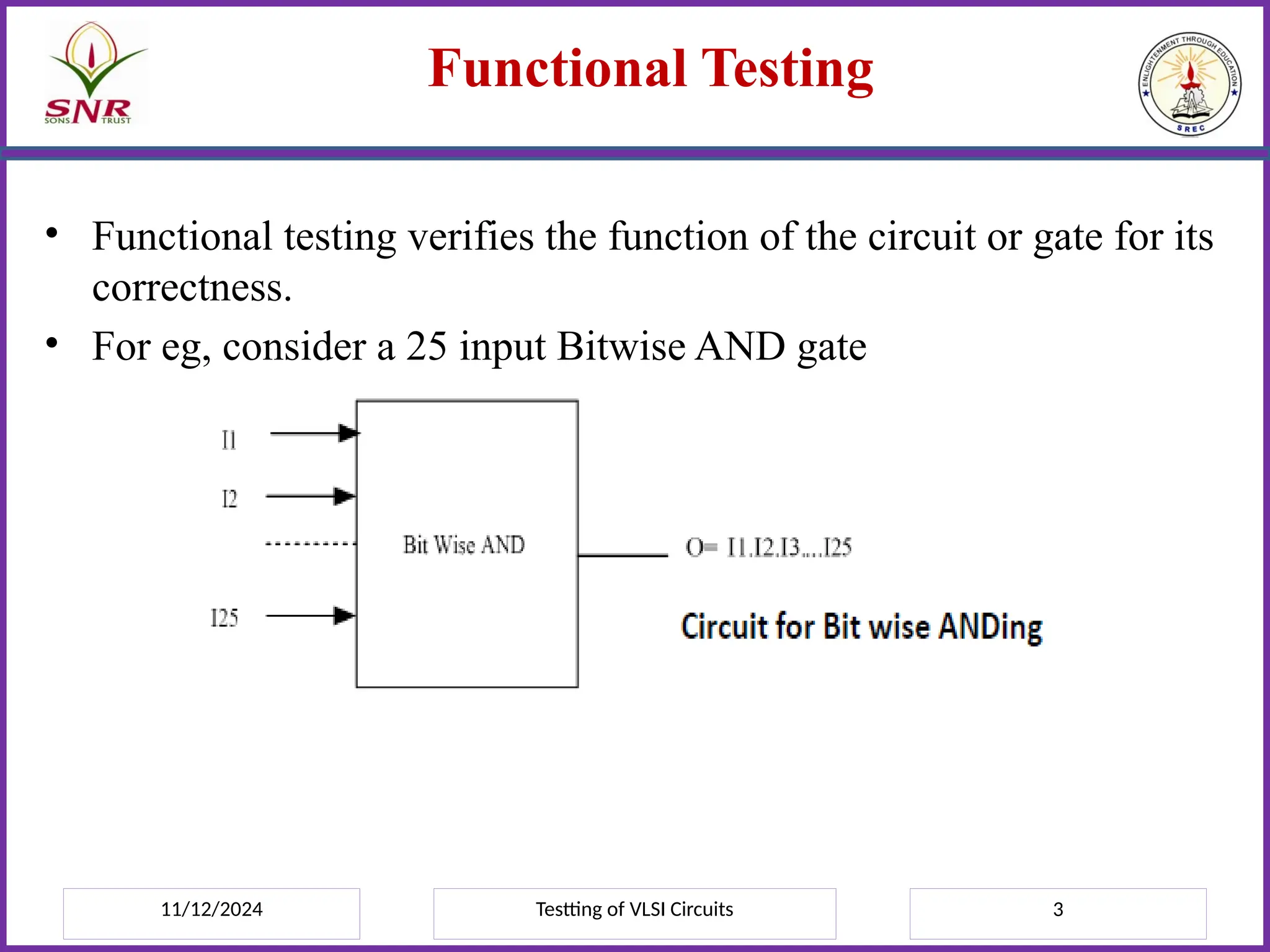
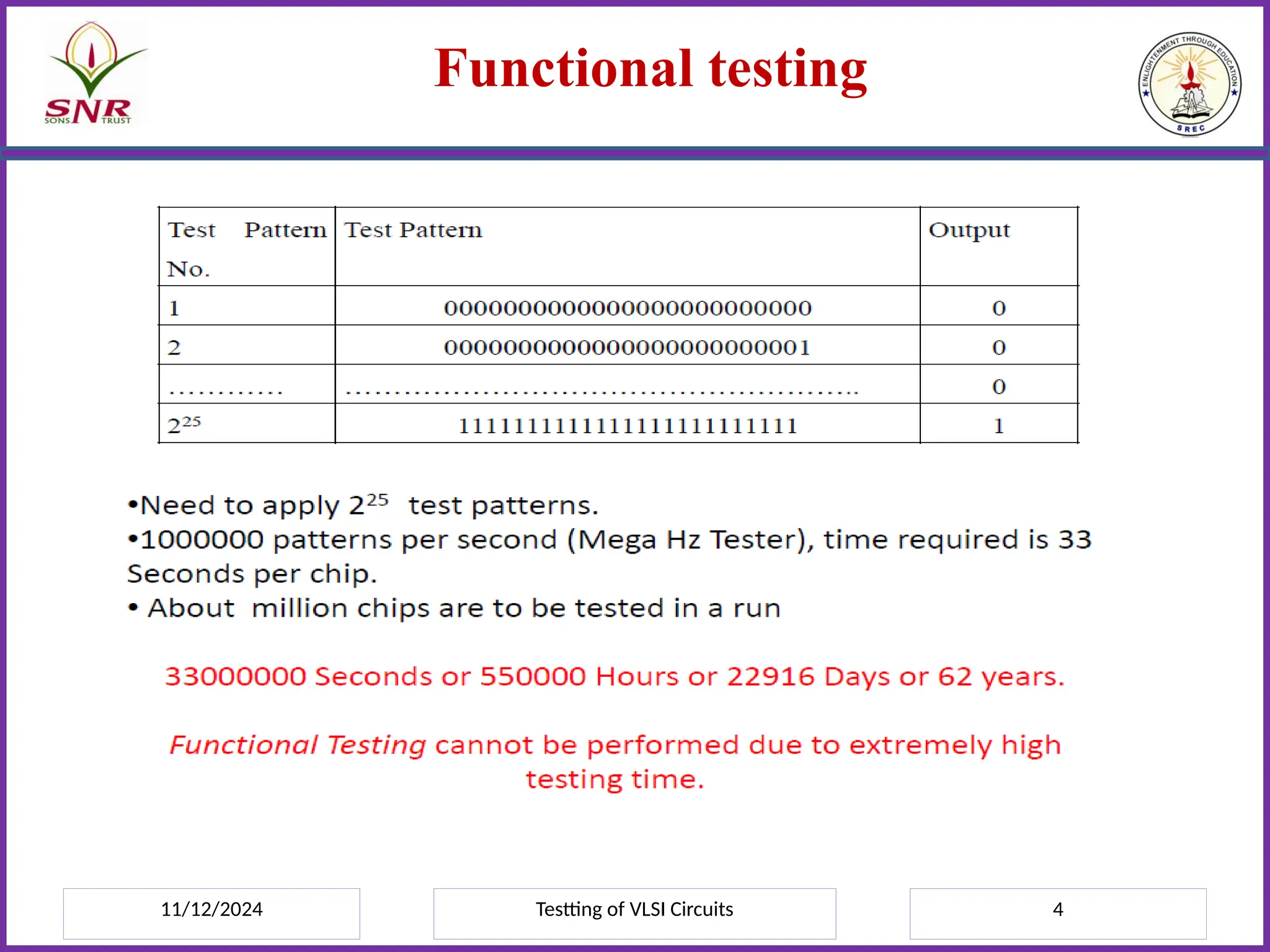
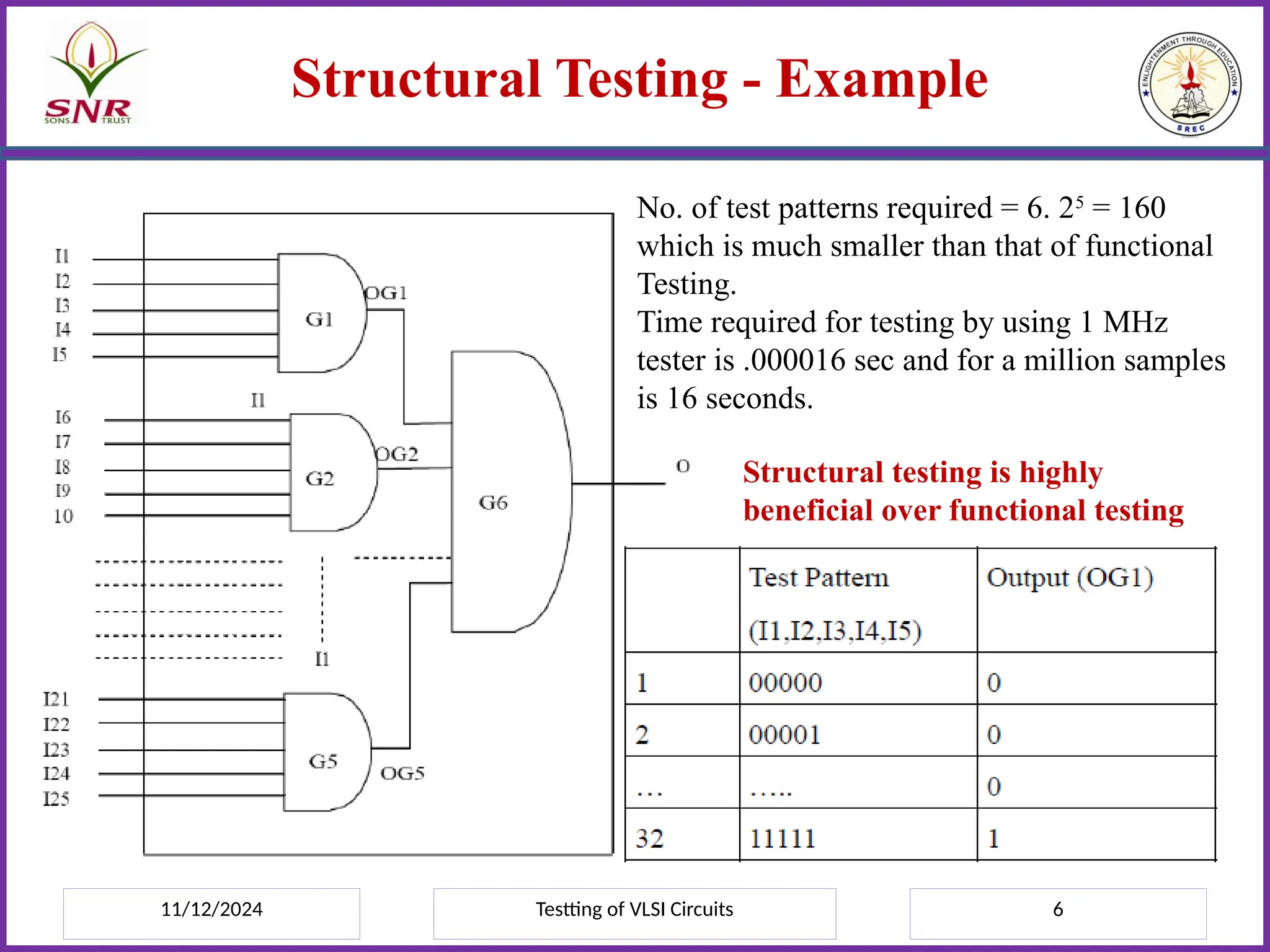
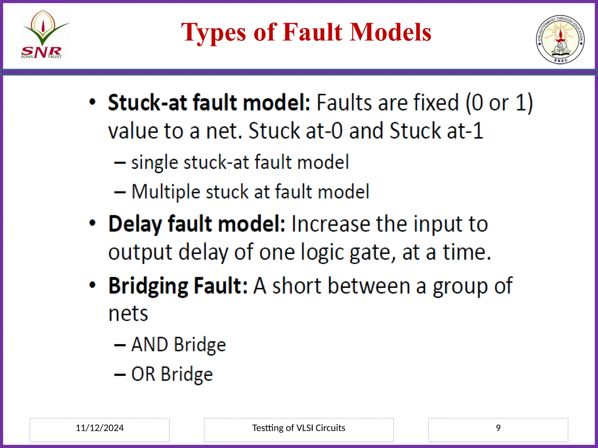
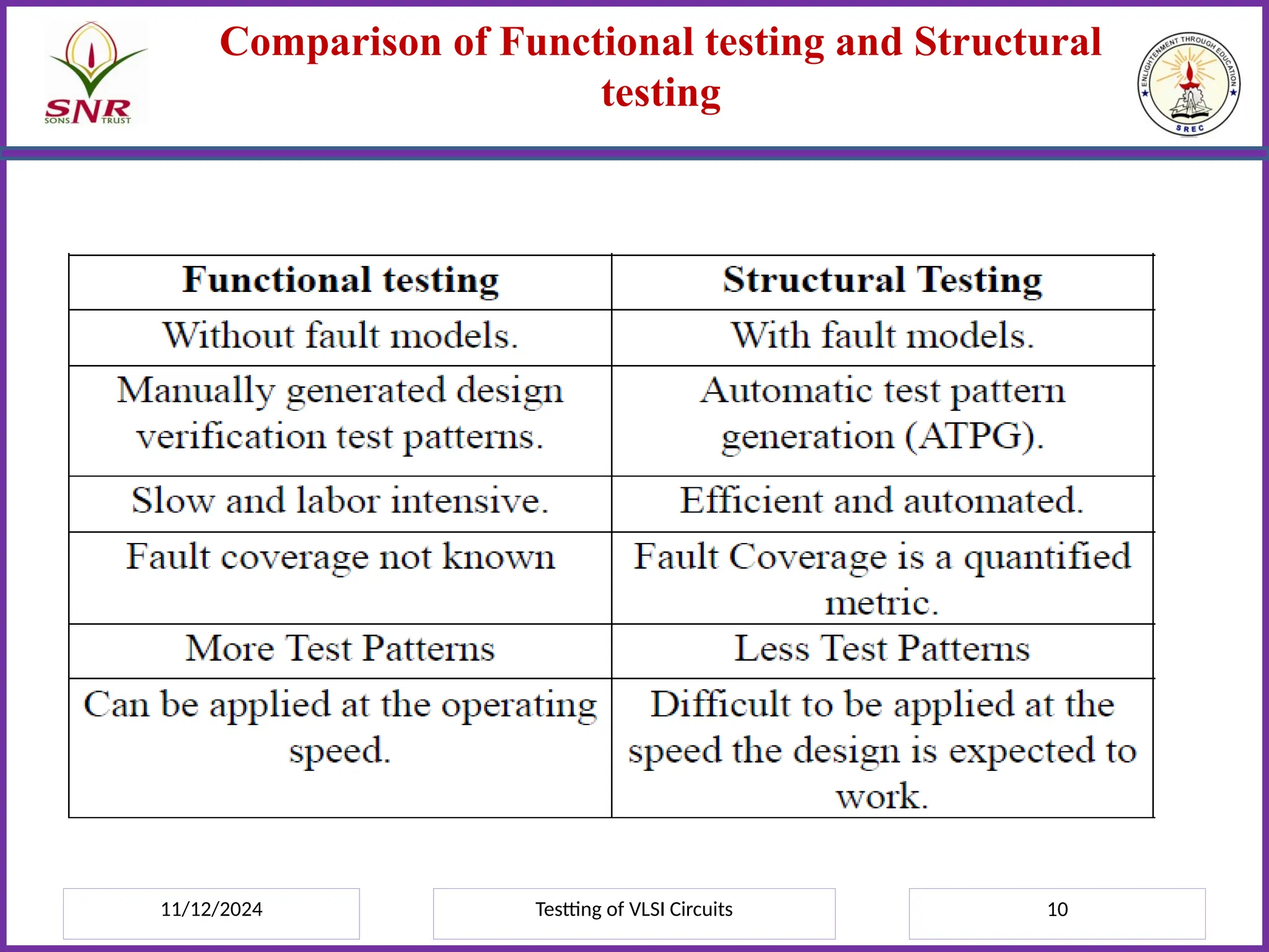
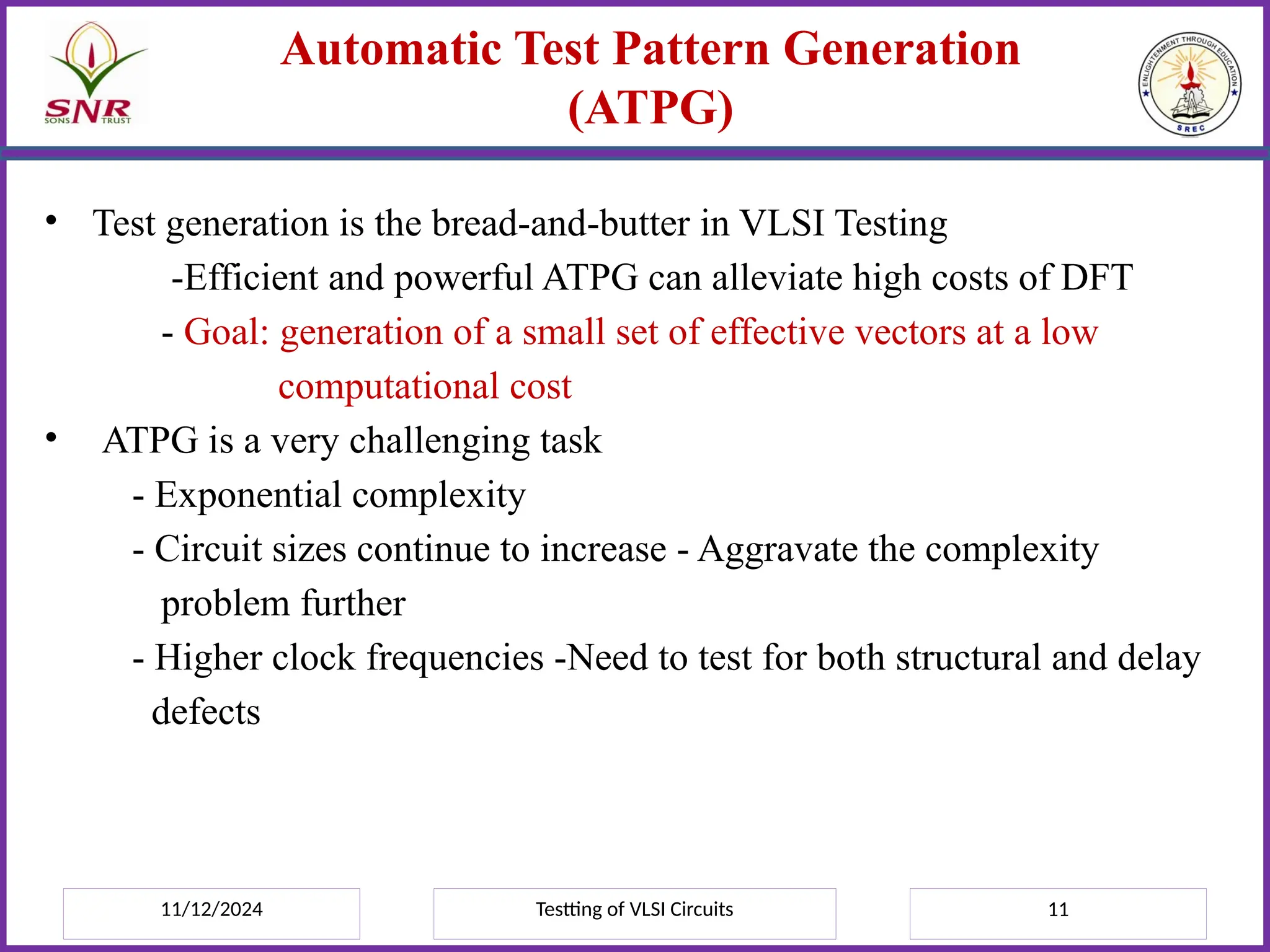
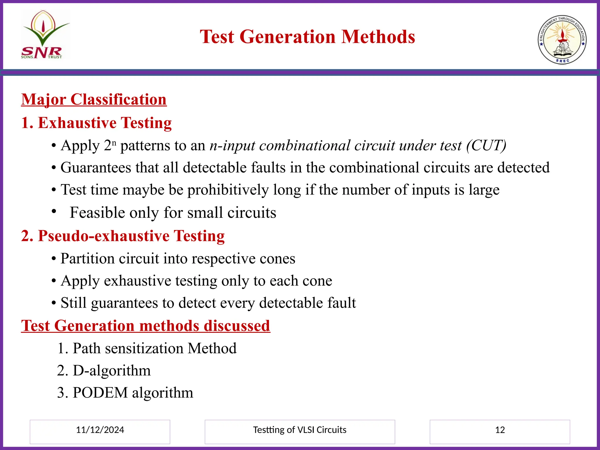
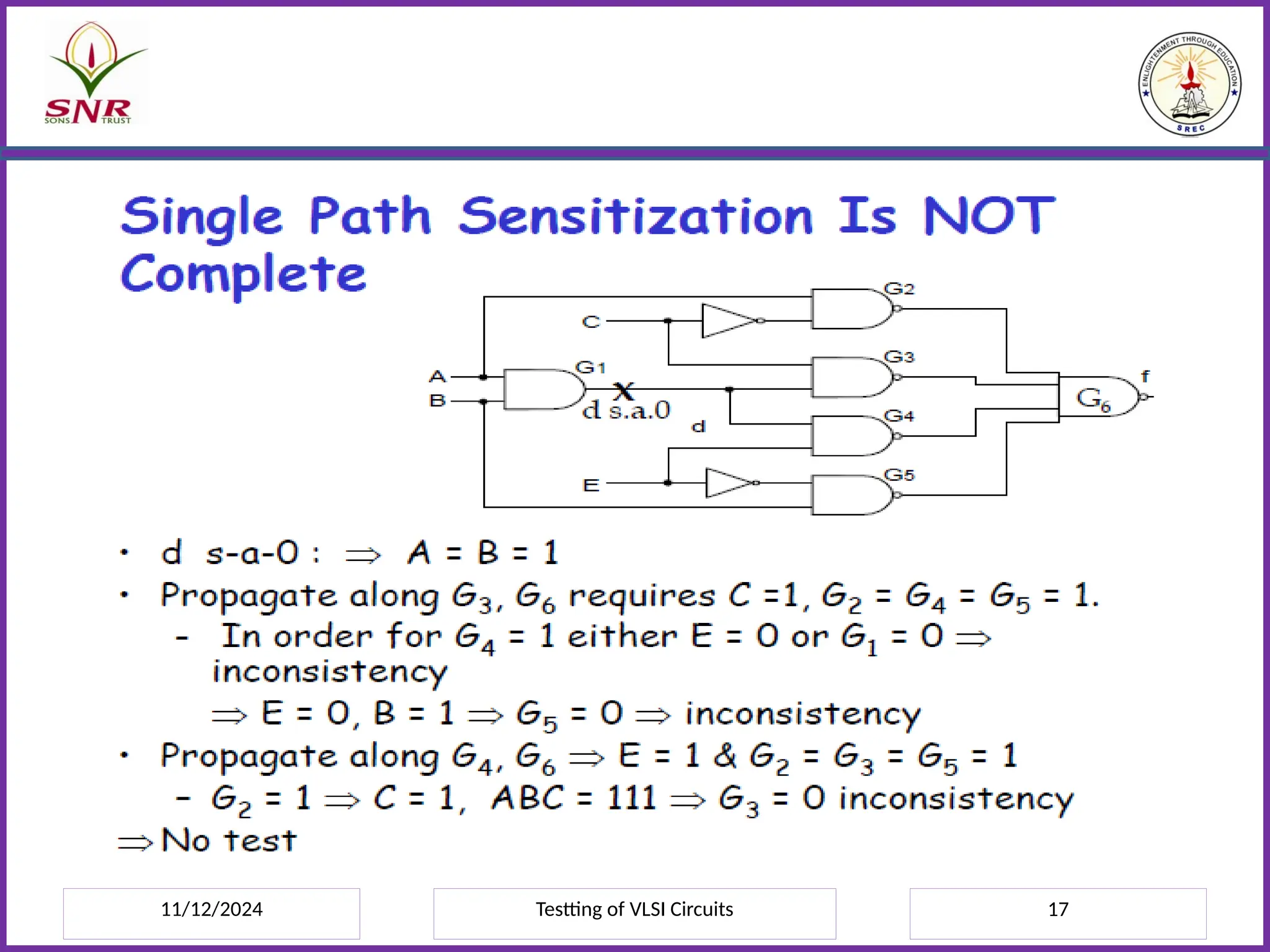
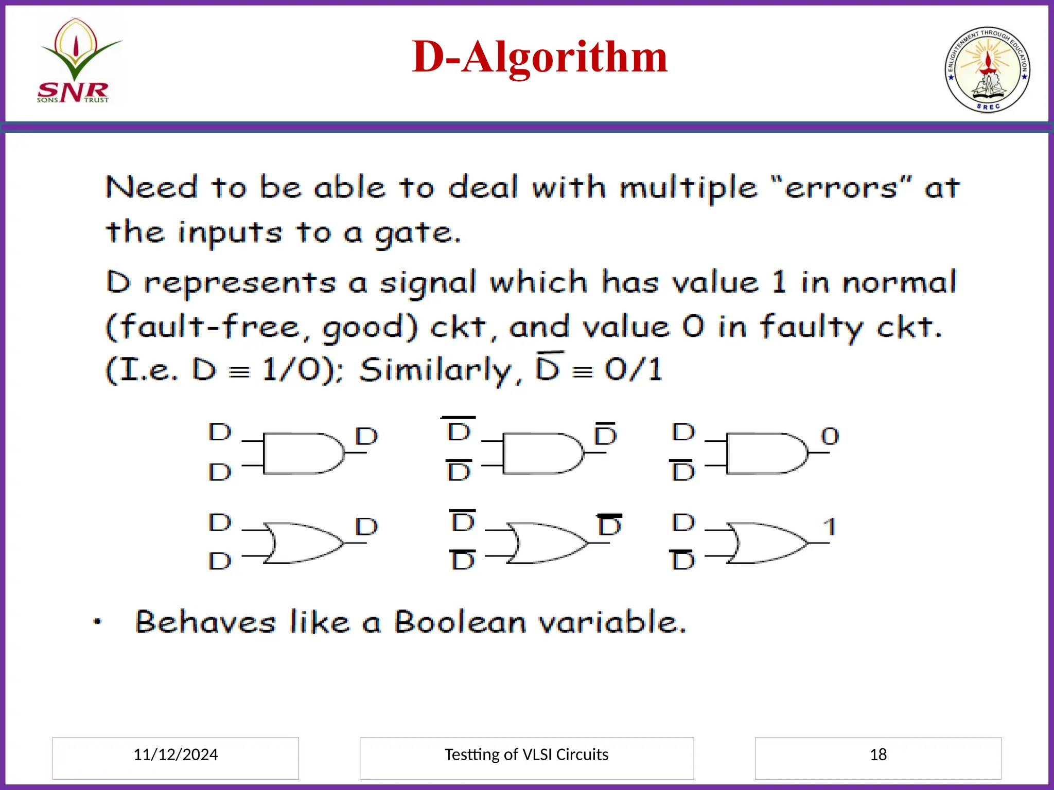
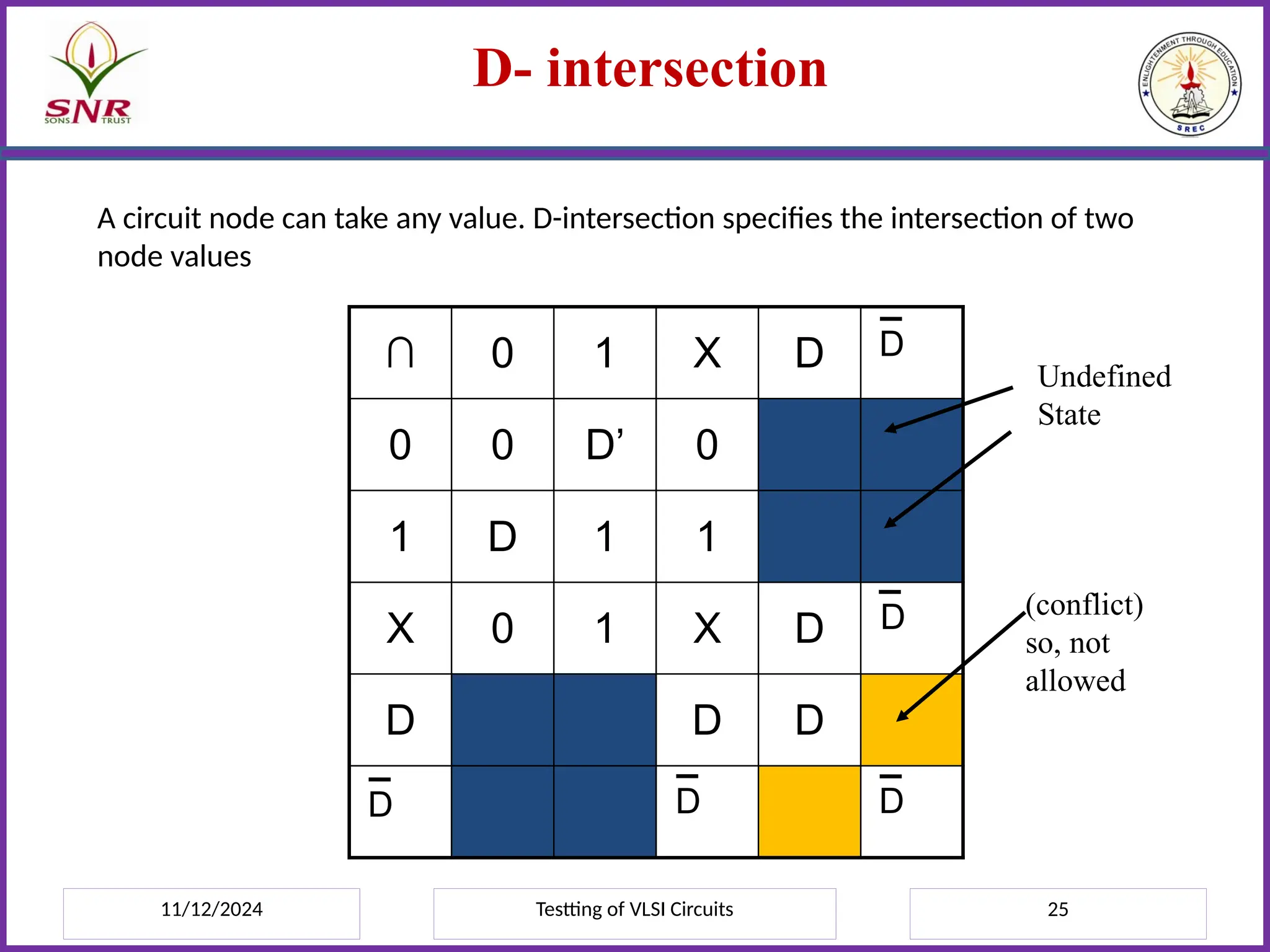
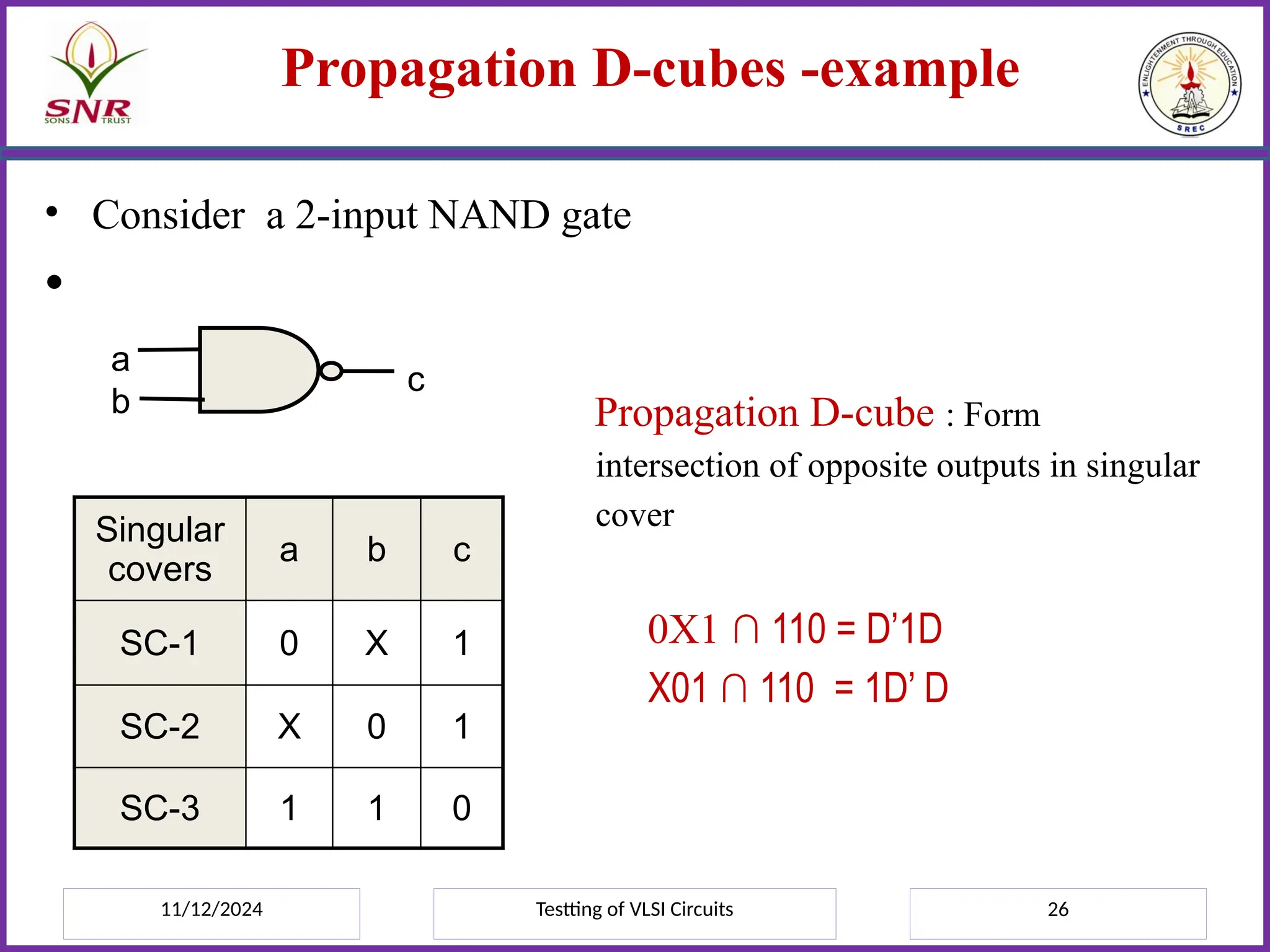
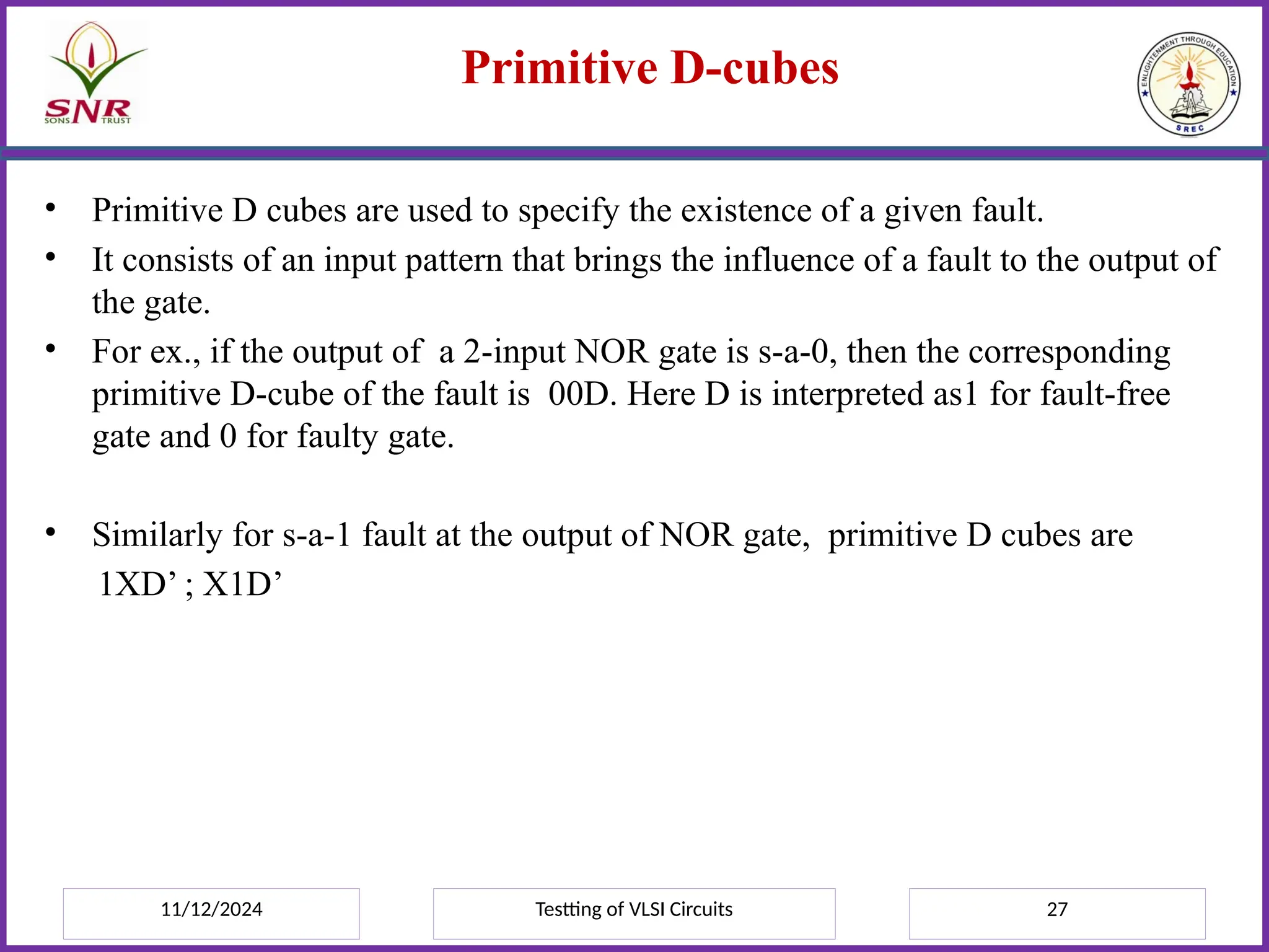
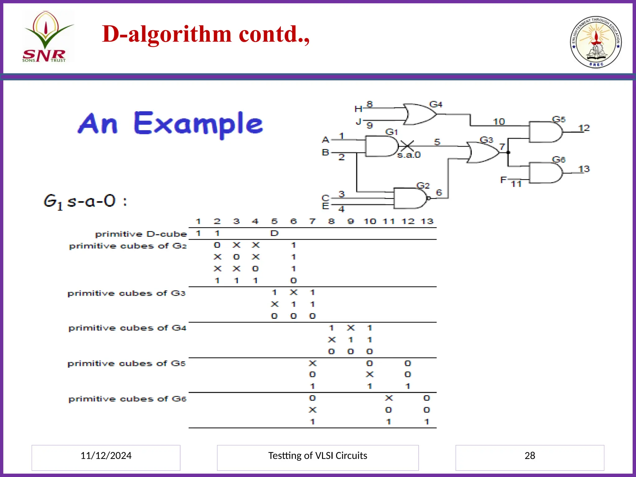
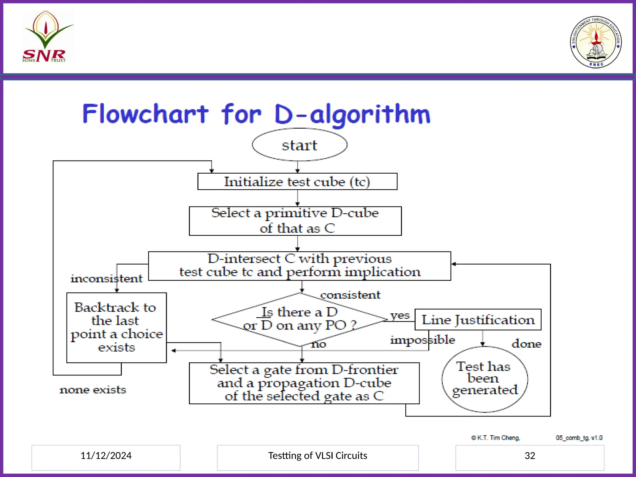
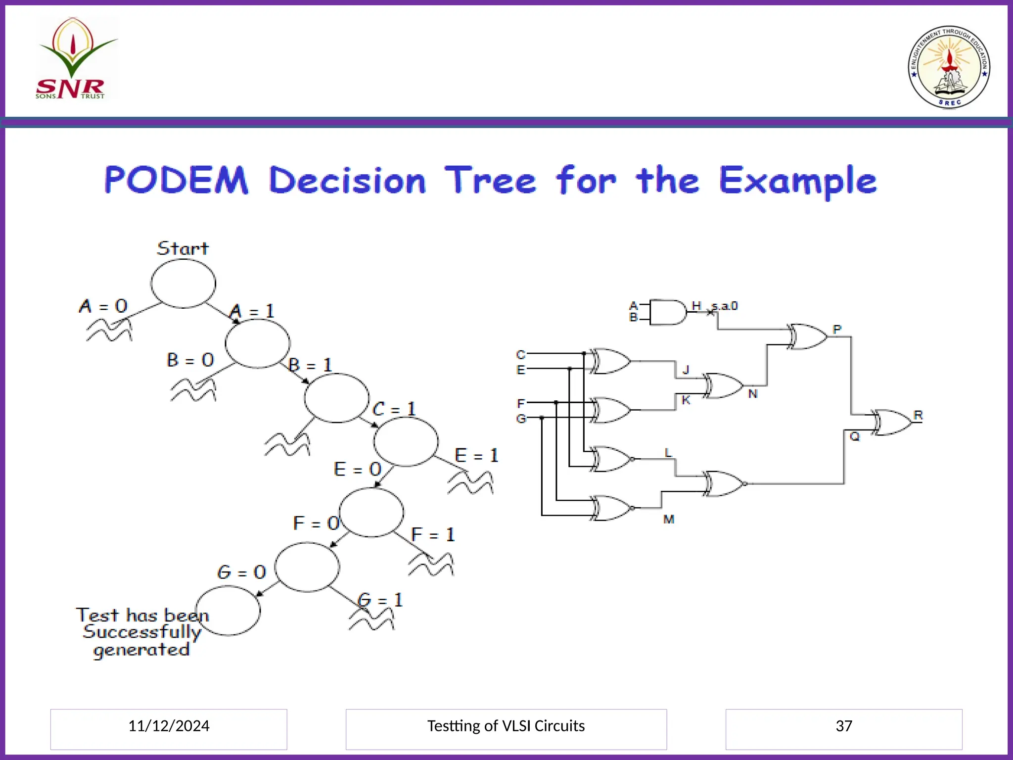
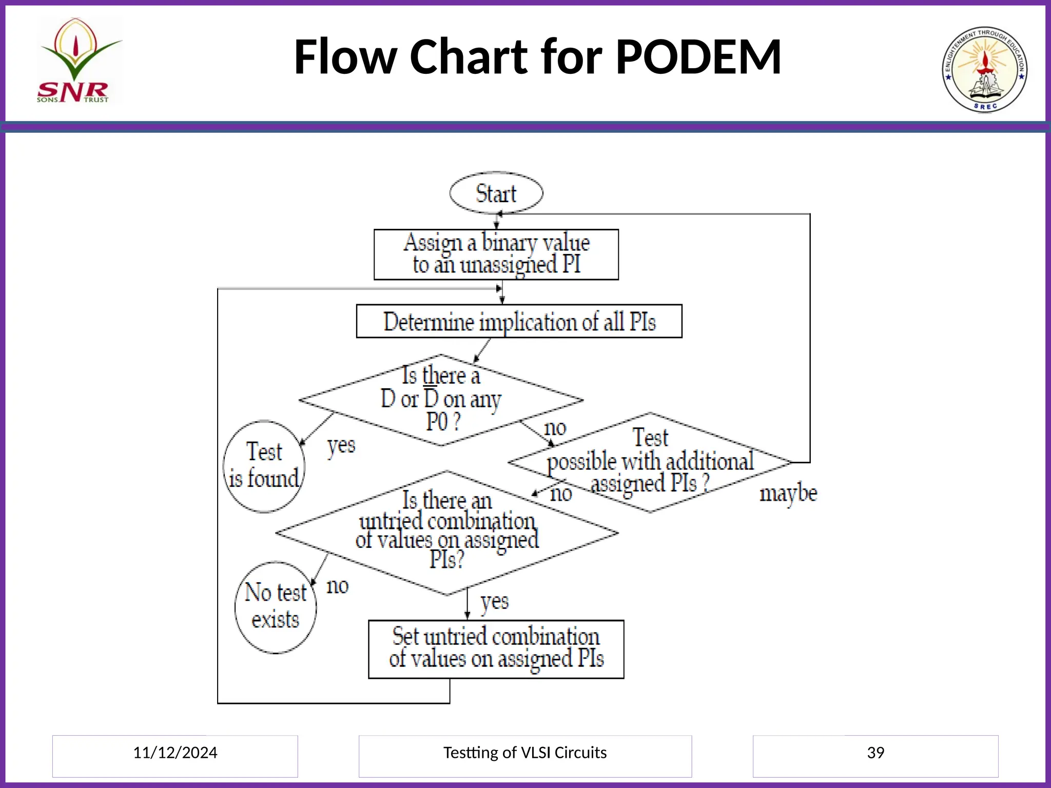
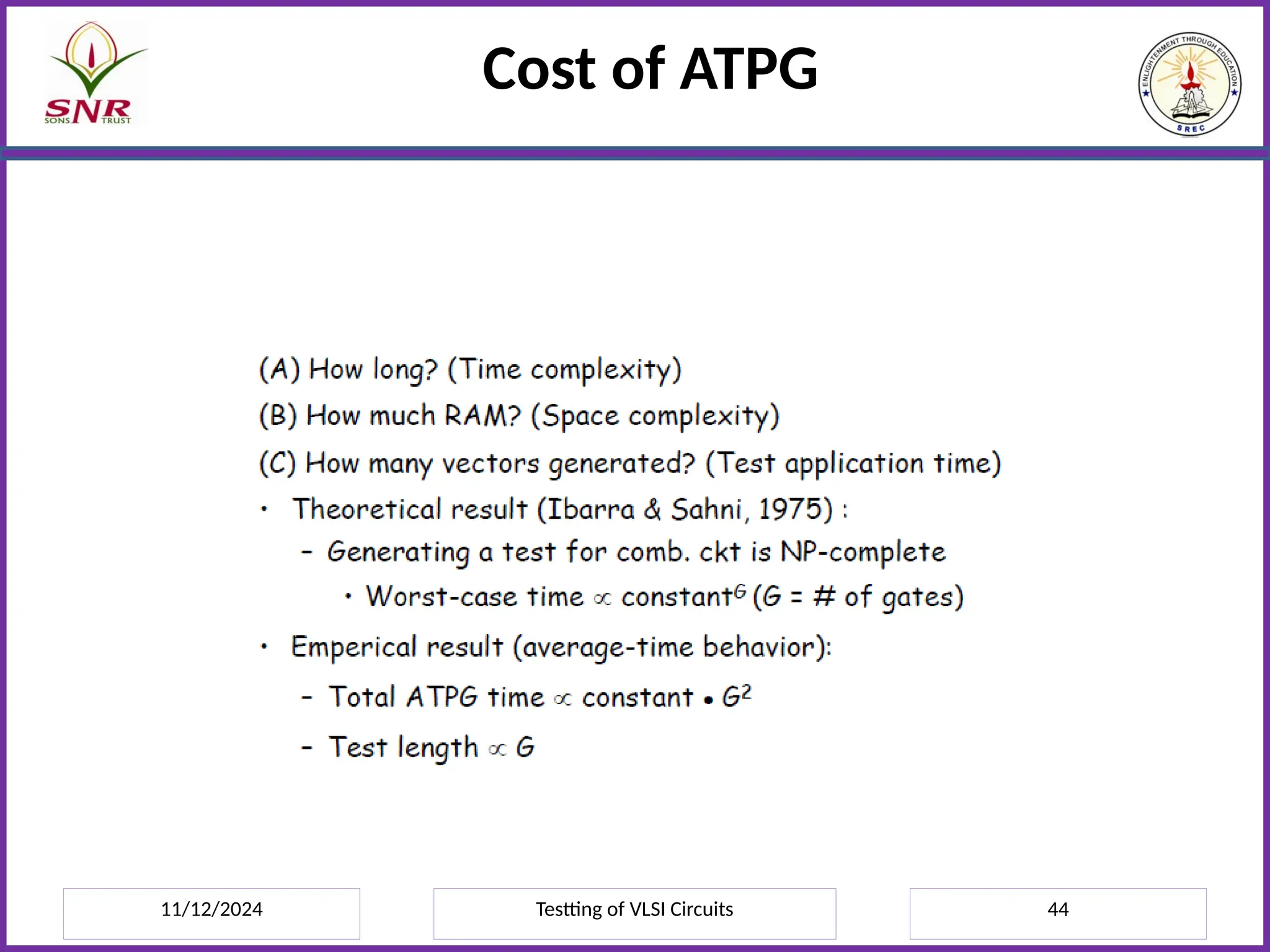
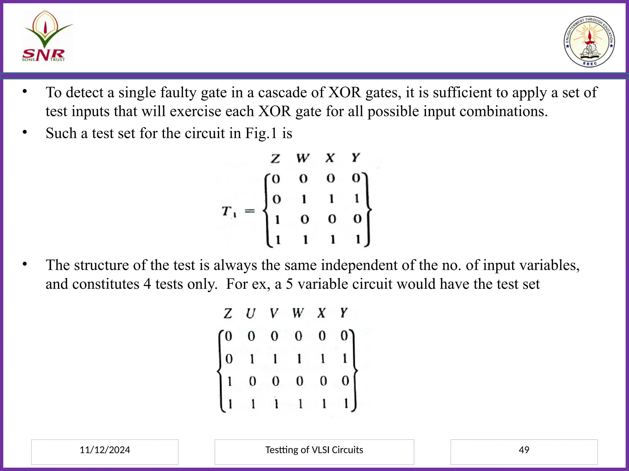
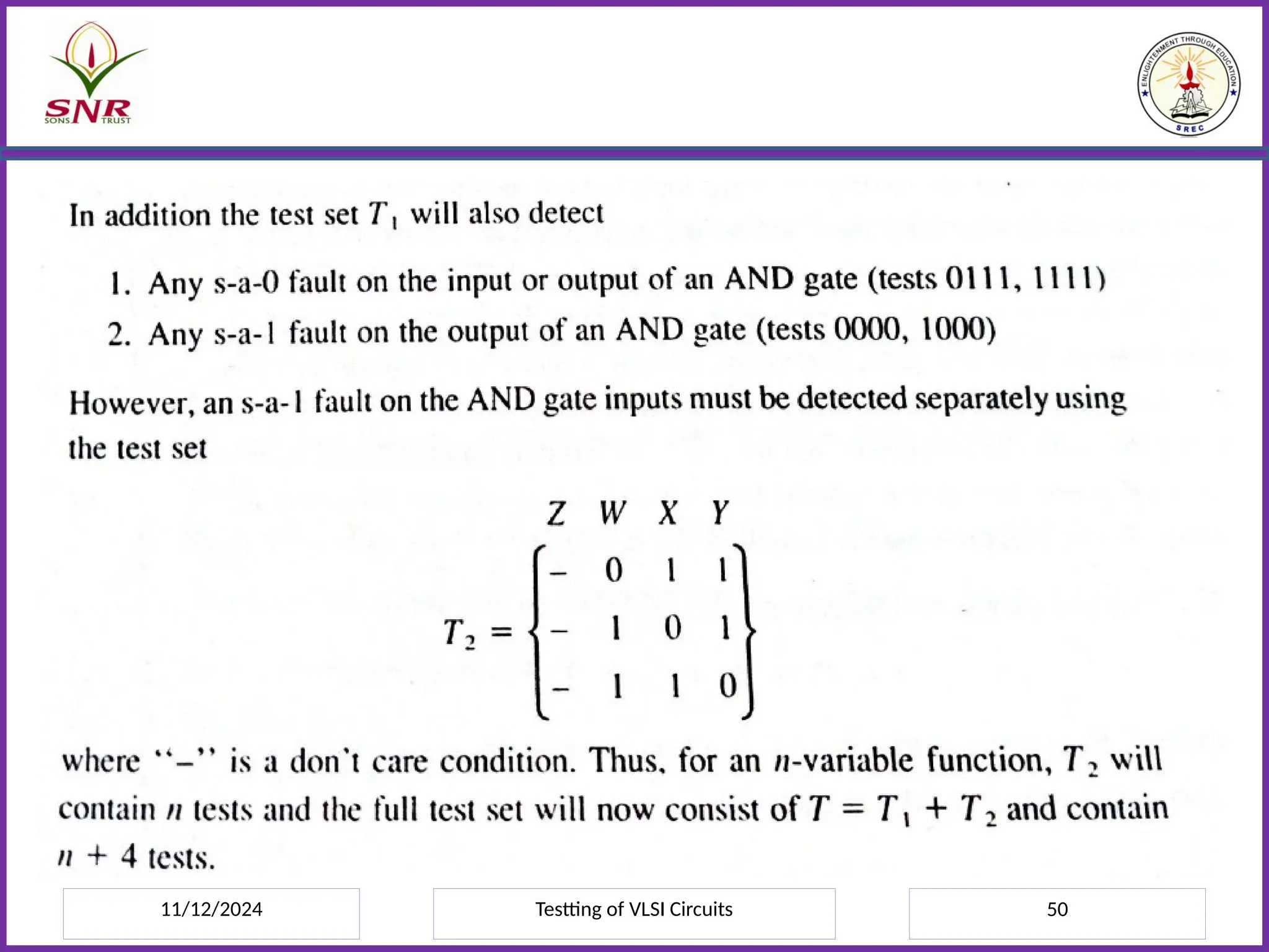
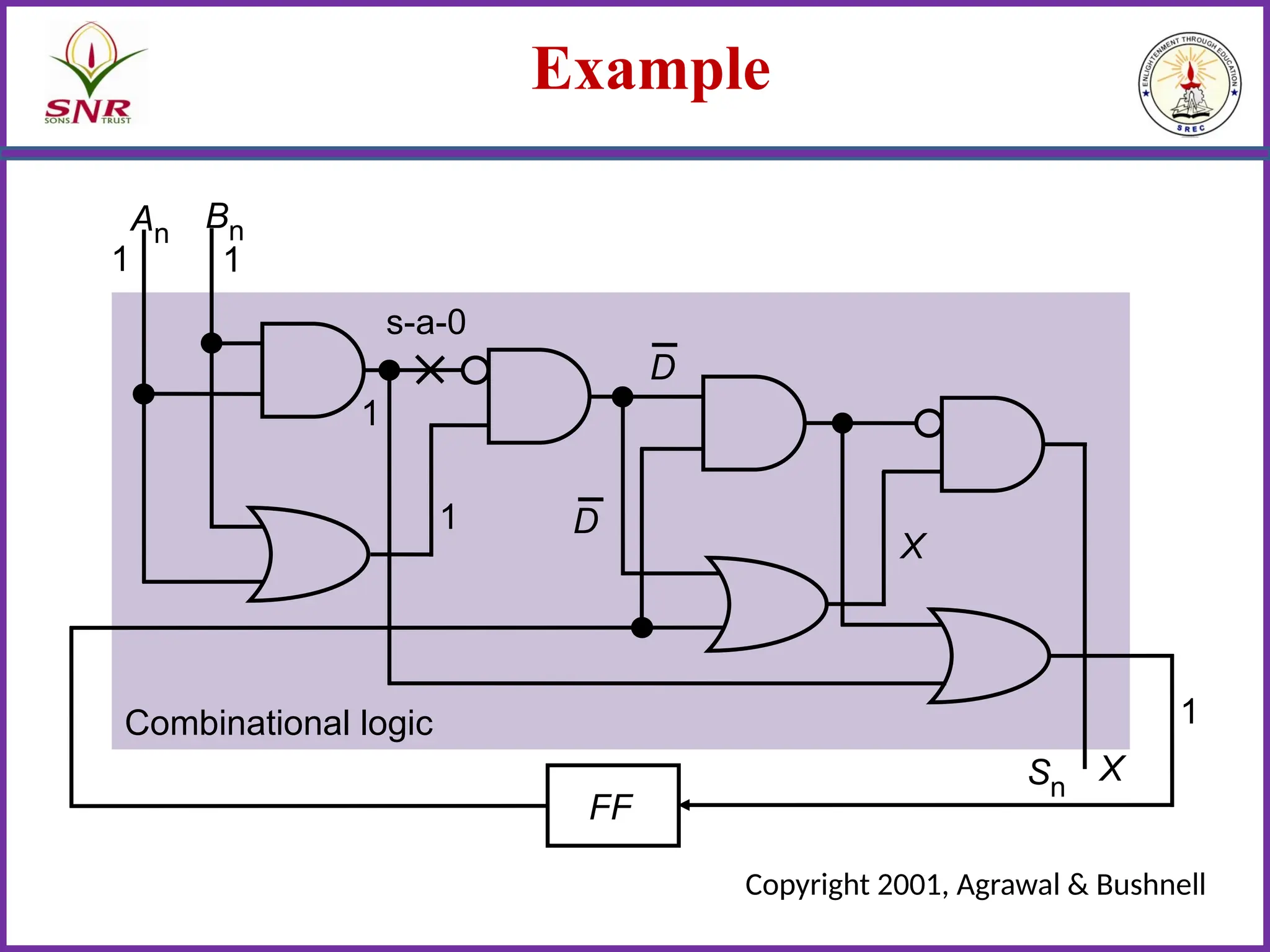
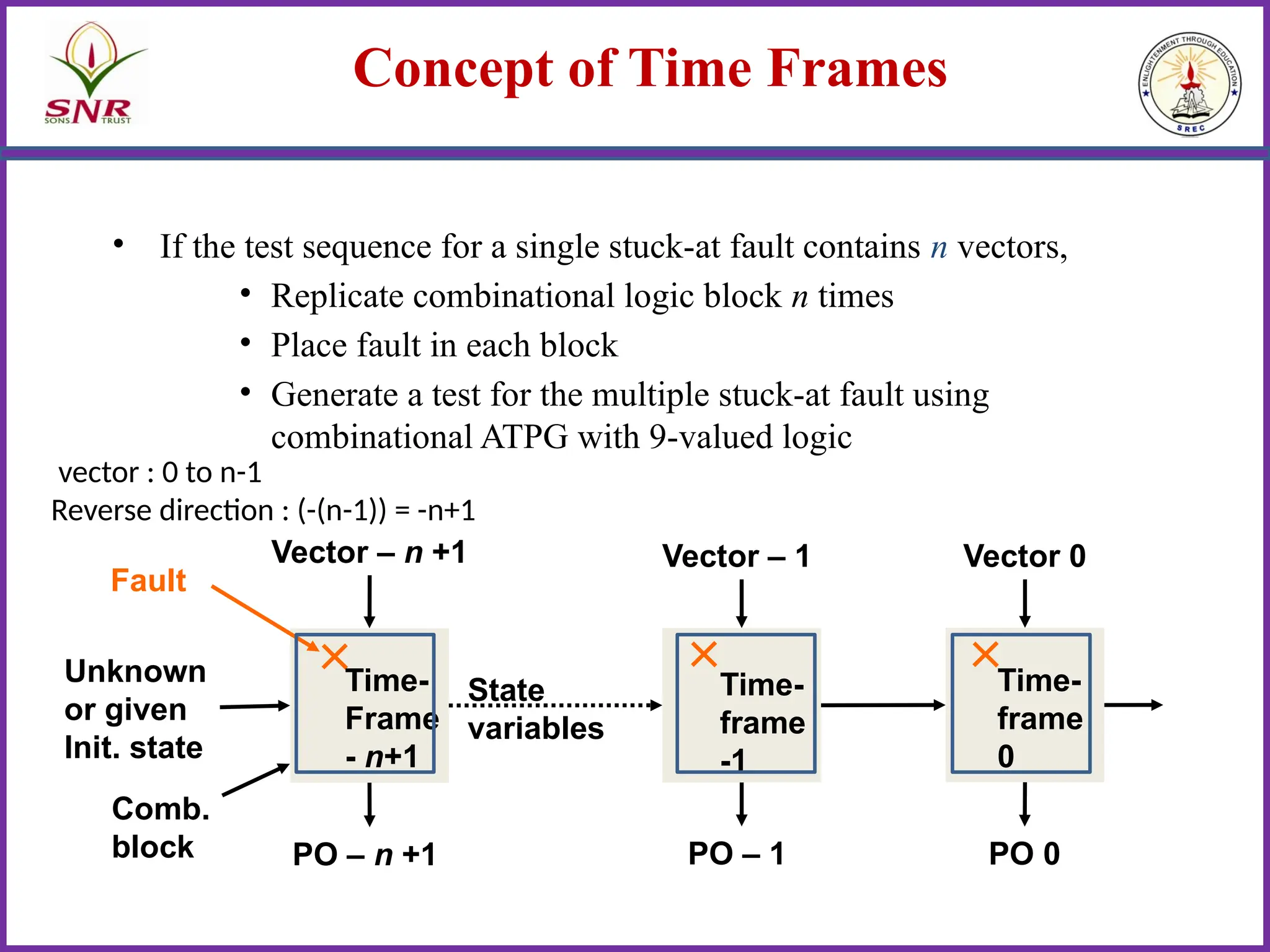
SRI RAMAKRISHNA ENGINEERING COLLEGE
VATTAMALAIPALAYAM, N.G.G.O. COLONY POST,
COIMBATORE – 641 022.
Module 2
Test Generation -Part 1
Combinational Circuits – Test Generation
11/12/2024 Testting of VLSI Circuits 2
Review of Functional and
Structural testing
11/12/2024 Testting of VLSI Circuits 3
Functional Testing
• Functional testing verifies the function of the circuit or gate for its
correctness.
• For eg, consider a 25 input Bitwise AND gate
11/12/2024 Testting of VLSI Circuits 4
Functional testing
11/12/2024 Testting of VLSI Circuits 5
Structural Testing
11/12/2024 Testting of VLSI Circuits 6
Structural Testing - Example
No. of test patterns required = 6. 25
= 160
which is much smaller than that of functional
Testing.
Time required for testing by using 1 MHz
tester is .000016 sec and for a million samples
is 16 seconds.
Structural testing is highly
beneficial over functional testing
11/12/2024 Testting of VLSI Circuits 7
Structural Testing - Penalties
Efficient structural testing is the one with less no. of on-chip
components and yet maintaining the quality of test solution.
Structural testing with fault models is the answer to the
requirement.
11/12/2024 Testting of VLSI Circuits 8
Structural Testing with fault models
11/12/2024 Testting of VLSI Circuits 9
Types of Fault Models
11/12/2024 Testting of VLSI Circuits 10
Comparison of Functional testing and Structural
testing
11/12/2024 Testting of VLSI Circuits 11
Automatic Test Pattern Generation
(ATPG)
• Test generation is the bread-and-butter in VLSI Testing
-Efficient and powerful ATPG can alleviate high costs of DFT
- Goal: generation of a small set of effective vectors at a low
computational cost
• ATPG is a very challenging task
- Exponential complexity
- Circuit sizes continue to increase - Aggravate the complexity
problem further
- Higher clock frequencies -Need to test for both structural and delay
defects
11/12/2024 Testting of VLSI Circuits 12
Test Generation Methods
Major Classification
1. Exhaustive Testing
• Apply 2n
patterns to an n-input combinational circuit under test (CUT)
• Guarantees that all detectable faults in the combinational circuits are detected
• Test time maybe be prohibitively long if the number of inputs is large
• Feasible only for small circuits
2. Pseudo-exhaustive Testing
• Partition circuit into respective cones
• Apply exhaustive testing only to each cone
• Still guarantees to detect every detectable fault
Test Generation methods discussed
1. Path sensitization Method
2. D-algorithm
3. PODEM algorithm
11/12/2024 Testting of VLSI Circuits 13
Path Sensitization Method
Basic steps:
1. Fault activation/sensitization/excitation :Specify inputs so as to generate
the appropriate value at fault site for fault excitation . (ie., set S to 1 for
Stuck-at-0 fault and set S to 0 for stuck-at-1 fault)
2. Fault propagation: specify additional signal values to propagate the fault
effect from the fault site to the outputs/observation points.
3. Line justification: Specify input values so as to produce the signal values
specified in (1) or (2)
4. Value implication: unique determination of values at other signals due to
value assignments made in (1), (2), or (3)
11/12/2024 Testting of VLSI Circuits 14
Example 1
G4
G3=0,E=0
11/12/2024 Testting of VLSI Circuits 15
Example 2
11/12/2024 Testting of VLSI Circuits 16
Completeness of ATPG Agorithms
11/12/2024 Testting of VLSI Circuits 17
11/12/2024 Testting of VLSI Circuits 18
D-Algorithm
11/12/2024 Testting of VLSI Circuits 19
D Algorithm
• Use D-algebra
• Activate fault
• Place a D or at fault site
• Do justification, forward implication and consistency check for all
signals
• Repeatedly propagate D-chain toward POs through a gate
• Do justification, forward implication and consistency check for all
signals
• Backtrack if
• A conflict occurs, or
• D-frontier becomes a null set
• Stop when
• D or D at a PO, i.e., test found, or
• If search exhausted without a test, then no test possible
11/12/2024 Testting of VLSI Circuits 20
D-algorithm contd.,
1) Select a primitive D-cube of the fault
2) Implication and checking for inconsistency.
- If inconsistency occurs, go to (1).
3) D-drive: selects an element in D-frontier & attempts to propagate D or ( or D’) in
its inputs to its output.
- D-frontier consists of set of all elements whose output values are unspecified but
inputs have some signals with D or D’.
- D-drive is done by intersecting the test cube with a propagation D-cube of the
selected element.
- Backtrack, i.e. select another propagation D-cube, if intersection is null.
4) Implication of D-drive: perform implication for the new test cube.
5) Repeat 3) & 4) until faulty signal propagated to an output.
6) Line justification: Consistency check on input conditions required.
D
Testting of VLSI Circuits 21
Definitions of terms in D-algorithm
Singular cover
• Singular cover of a logic gate is basically a compact version of the truth table
using don’t care inputs X which may be either 0 or 1.
Primitive D-cubes
• Specifies the minimal input conditions which must be applied to a logic
element E in order to produce an error signal at the output of E.
Propagation D-cubes
• The propagation D-cubes of a logic element E specify minimal input conditions
which are required to propagate an error signal on an input (or inputs) to the
output of that element.
11/12/2024
11/12/2024 Testting of VLSI Circuits 22
Definitions
• Justification: Changing inputs of a gate if the present input values do not
justify the output value.
• Forward implication: Determination of the gate output value, which is X,
according to the input values.
• Consistency check: Verifying that the gate output is justifiable from the values
of inputs, which may have changed since the output was determined.
• D-frontier: Set of gates whose inputs have a D or D’, and the output is X.
11/12/2024 Testting of VLSI Circuits 23
Singular Cover
• A singular cover of a logic gate is the compact version of the truth table using
don’t care inputs X, which may be either 0 or 1. Each row in a singular cover is
called a singular cube.
• Used for:
• Line justification: determine gate inputs for specified output.
• Forward implication: determine gate output
Singular
covers
a b c
SC-1 0 X 1
SC-2 X 0 1
SC-3 1 1 0
a
b
c
a b c
0 0 1
0 1 1
1 0 1
1 1 0
Truth Table
11/12/2024 Testting of VLSI Circuits 24
Propagation D-cubes (PDC)
• Used for D-drive (propagation of D through gates) and forward
implication.
• PDC consists of a table for each circuit element which has entries for
propagating faults on any one of its inputs to the output.
• To generate PDC entry corresponding to any one column, D-intersect any
two rows of SC which have opposite vales(0 & 1) in that column.
• For ex, consider a AND gate
• SC : a b c To find pdc for a, consider c1 and c3 intersection
c1 0 X 0 pdc : D’ 1 D’
c2 X 0 0 Similarly for b, consider c2 and c3
c3 1 1 1 pdc ; 1 D’ D’
11/12/2024 Testting of VLSI Circuits 25
D- intersection
∩ 0 1 X D
0 0 D’ 0
1 D 1 1
X 0 1 X D
D D D
D
D
D
D D
Undefined
State
(conflict)
so, not
allowed
A circuit node can take any value. D-intersection specifies the intersection of two
node values
11/12/2024 Testting of VLSI Circuits 26
Propagation D-cubes -example
• Consider a 2-input NAND gate
•
Propagation D-cube : Form
intersection of opposite outputs in singular
cover
0X1 ∩ 110 = D’1D
X01 ∩ 110 = 1D’ D
a
b
c
Singular
covers
a b c
SC-1 0 X 1
SC-2 X 0 1
SC-3 1 1 0
11/12/2024 Testting of VLSI Circuits 27
Primitive D-cubes
• Primitive D cubes are used to specify the existence of a given fault.
• It consists of an input pattern that brings the influence of a fault to the output of
the gate.
• For ex., if the output of a 2-input NOR gate is s-a-0, then the corresponding
primitive D-cube of the fault is 00D. Here D is interpreted as1 for fault-free
gate and 0 for faulty gate.
• Similarly for s-a-1 fault at the output of NOR gate, primitive D cubes are
1XD’ ; X1D’
11/12/2024 Testting of VLSI Circuits 28
D-algorithm contd.,
11/12/2024 Testting of VLSI Circuits 29
Example
11/12/2024 Testting of VLSI Circuits 30
11/12/2024 Testting of VLSI Circuits 31
11/12/2024 Testting of VLSI Circuits 32
11/12/2024 Testting of VLSI Circuits 33
11/12/2024 Testting of VLSI Circuits 34
11/12/2024 Testting of VLSI Circuits 35
11/12/2024 Testting of VLSI Circuits 36
Path Oriented Decision Making
(PODEM)
11/12/2024 Testting of VLSI Circuits 37
11/12/2024 Testting of VLSI Circuits 38
11/12/2024 Testting of VLSI Circuits 39
Flow Chart for PODEM
11/12/2024 Testting of VLSI Circuits 40
Steps in PODEM
11/12/2024 Testting of VLSI Circuits 41
Flow Chart of Backtrace
11/12/2024 Testting of VLSI Circuits 42
Example
11/12/2024 Testting of VLSI Circuits 43
11/12/2024 Testting of VLSI Circuits 44
Cost of ATPG
11/12/2024 Testting of VLSI Circuits 45
Testable Combinational Logic circuit design
• A logic circuit is considered to be testable if it is easy to generate a set of
test patterns to achieve high fault coverage in the circuit..
Reed-Muller Expansion Technique
This technique can be used to design any arbitrary n-variable Boolean
function using AND & XOR gates only. The circuit so designed has the
following properties.
Properties :
1. If the primary input leads are fault-free, then at most n+4 tests are
required to detect all single stuck-at faults in the circuit.
2. If there are faults on the primary leads as well, then the number of tests
required is (n+4)+2nc, where nc is the no. of input variables that appear
even no. of times in the product terms of Reed-Muller expansion.
11/12/2024 Testting of VLSI Circuits 46
• But, by adding an extra AND gate with its output being made
observable, the additional 2n tests can be removed. The input to the
AND gate are those inputs appearing an even number of times in the
Reed-Muller expansion.
• Any combinational function of n variables can be described by a Reed-
Muller expansion of the form
11/12/2024 Testting of VLSI Circuits 47
• For a three-variable function, the Reed-Muller expansion is
• The constants Ci may be computed by using the following properties of
XOR operation:
• Example: To illustrate, consider the Boolean function
11/12/2024 Testting of VLSI Circuits 48
• A direct implementation of the function is shown in Fig.1.
11/12/2024 Testting of VLSI Circuits 49
• To detect a single faulty gate in a cascade of XOR gates, it is sufficient to apply a set of
test inputs that will exercise each XOR gate for all possible input combinations.
• Such a test set for the circuit in Fig.1 is
• The structure of the test is always the same independent of the no. of input variables,
and constitutes 4 tests only. For ex, a 5 variable circuit would have the test set
11/12/2024 Testting of VLSI Circuits 50
11/12/2024 Testting of VLSI Circuits 51
Sequential Circuits – Test Generation
Sequential Circuits
• A sequential circuit has memory in addition to combinational logic.
• Test for a fault in a sequential circuit is a sequence of vectors, which
• Initializes the circuit to a known state
• Activates the fault, and
• Propagates the fault effect to a primary output
• Methods of sequential circuit ATPG
• Time-frame expansion methods
• Simulation-based methods
Copyright 2001, Agrawal & Bushnell
Example
FF
An
Bn
Sn
s-a-0
1
1
1
1
1
X
X
D
D
Combinational logic
Copyright 2001, Agrawal & Bushnell
Concept of Time Frames
• If the test sequence for a single stuck-at fault contains n vectors,
• Replicate combinational logic block n times
• Place fault in each block
• Generate a test for the multiple stuck-at fault using
combinational ATPG with 9-valued logic
Comb.
block
Fault
Time-
frame
0
Time-
frame
-1
Time-
Frame
- n+1
Unknown
or given
Init. state
Vector 0
Vector – 1
Vector – n +1
PO 0
PO – 1
PO – n +1
State
variables
vector : 0 to n-1
Reverse direction : (-(n-1)) = -n+1
Time Frame Expansion
An Bn
FF
Cn
Cn+1
1
X
X
Sn
s-a-0
1
1
1
1
D
D
Combinational logic
Sn-1
s-a-0
1
1
1
1 X
D
D
Combinational logic
1
D
D
X
An-1
Bn-1
Time-frame -1 Time-frame 0
Copyright 2001, Agrawal & Bushnell
Nine-Valued Logic D-Algorithm
(Muth, IEEE TC, June 1976)
• 9- valued logic : values under fault-free/faulty conditions , so for values
0,1 and X , we have 9 possibilities.
• Ordered pairs of states of the fault-free and faulty circuits (0/0, 0/1, 0/X,
1/0, 1/1, 1/X, X/0, X/1, X/X) are used
• A superset of the five values (0=0/0, 1=1/1, X=X/X, D=1/0, D=0/1) used
in the D-Algorithm
• Take into account the possible repeated effects of the fault in the
iterative array model
Nine valued logic
A
B
X
X
X
0
s-a-1
0/1
A
B
0/X 0/X
0/1
X
s-a-1
X/1
FF1 FF1
FF2 FF2
0/1 X/1
Good faulty
Implementation of ATPG
• Select a PO (primary output) for fault detection based on drivability analysis.
• Place a logic value, 1/0 or 0/1, depending on fault type and number of
inversions.
• Justify the output value from PIs, considering all necessary paths and adding
backward time-frames.
• If justification is impossible, then use drivability to select another PO and
repeat justification.
• If the procedure fails for all reachable POs, then the fault is untestable.
• If 1/0 or 0/1 cannot be justified at any PO, but 1/X or 0/X can be justified, then
the fault is potentially detectable.
Summary: Test Complexity is high for sequential circuits

Module 2 -Test Generation VLSI DESIGN .pptx

  • 1.
    SRI RAMAKRISHNA ENGINEERINGCOLLEGE VATTAMALAIPALAYAM, N.G.G.O. COLONY POST, COIMBATORE – 641 022. Module 2 Test Generation -Part 1 Combinational Circuits – Test Generation
  • 2.
    11/12/2024 Testting ofVLSI Circuits 2 Review of Functional and Structural testing
  • 3.
    11/12/2024 Testting ofVLSI Circuits 3 Functional Testing • Functional testing verifies the function of the circuit or gate for its correctness. • For eg, consider a 25 input Bitwise AND gate
  • 4.
    11/12/2024 Testting ofVLSI Circuits 4 Functional testing
  • 5.
    11/12/2024 Testting ofVLSI Circuits 5 Structural Testing
  • 6.
    11/12/2024 Testting ofVLSI Circuits 6 Structural Testing - Example No. of test patterns required = 6. 25 = 160 which is much smaller than that of functional Testing. Time required for testing by using 1 MHz tester is .000016 sec and for a million samples is 16 seconds. Structural testing is highly beneficial over functional testing
  • 7.
    11/12/2024 Testting ofVLSI Circuits 7 Structural Testing - Penalties Efficient structural testing is the one with less no. of on-chip components and yet maintaining the quality of test solution. Structural testing with fault models is the answer to the requirement.
  • 8.
    11/12/2024 Testting ofVLSI Circuits 8 Structural Testing with fault models
  • 9.
    11/12/2024 Testting ofVLSI Circuits 9 Types of Fault Models
  • 10.
    11/12/2024 Testting ofVLSI Circuits 10 Comparison of Functional testing and Structural testing
  • 11.
    11/12/2024 Testting ofVLSI Circuits 11 Automatic Test Pattern Generation (ATPG) • Test generation is the bread-and-butter in VLSI Testing -Efficient and powerful ATPG can alleviate high costs of DFT - Goal: generation of a small set of effective vectors at a low computational cost • ATPG is a very challenging task - Exponential complexity - Circuit sizes continue to increase - Aggravate the complexity problem further - Higher clock frequencies -Need to test for both structural and delay defects
  • 12.
    11/12/2024 Testting ofVLSI Circuits 12 Test Generation Methods Major Classification 1. Exhaustive Testing • Apply 2n patterns to an n-input combinational circuit under test (CUT) • Guarantees that all detectable faults in the combinational circuits are detected • Test time maybe be prohibitively long if the number of inputs is large • Feasible only for small circuits 2. Pseudo-exhaustive Testing • Partition circuit into respective cones • Apply exhaustive testing only to each cone • Still guarantees to detect every detectable fault Test Generation methods discussed 1. Path sensitization Method 2. D-algorithm 3. PODEM algorithm
  • 13.
    11/12/2024 Testting ofVLSI Circuits 13 Path Sensitization Method Basic steps: 1. Fault activation/sensitization/excitation :Specify inputs so as to generate the appropriate value at fault site for fault excitation . (ie., set S to 1 for Stuck-at-0 fault and set S to 0 for stuck-at-1 fault) 2. Fault propagation: specify additional signal values to propagate the fault effect from the fault site to the outputs/observation points. 3. Line justification: Specify input values so as to produce the signal values specified in (1) or (2) 4. Value implication: unique determination of values at other signals due to value assignments made in (1), (2), or (3)
  • 14.
    11/12/2024 Testting ofVLSI Circuits 14 Example 1 G4 G3=0,E=0
  • 15.
    11/12/2024 Testting ofVLSI Circuits 15 Example 2
  • 16.
    11/12/2024 Testting ofVLSI Circuits 16 Completeness of ATPG Agorithms
  • 17.
    11/12/2024 Testting ofVLSI Circuits 17
  • 18.
    11/12/2024 Testting ofVLSI Circuits 18 D-Algorithm
  • 19.
    11/12/2024 Testting ofVLSI Circuits 19 D Algorithm • Use D-algebra • Activate fault • Place a D or at fault site • Do justification, forward implication and consistency check for all signals • Repeatedly propagate D-chain toward POs through a gate • Do justification, forward implication and consistency check for all signals • Backtrack if • A conflict occurs, or • D-frontier becomes a null set • Stop when • D or D at a PO, i.e., test found, or • If search exhausted without a test, then no test possible
  • 20.
    11/12/2024 Testting ofVLSI Circuits 20 D-algorithm contd., 1) Select a primitive D-cube of the fault 2) Implication and checking for inconsistency. - If inconsistency occurs, go to (1). 3) D-drive: selects an element in D-frontier & attempts to propagate D or ( or D’) in its inputs to its output. - D-frontier consists of set of all elements whose output values are unspecified but inputs have some signals with D or D’. - D-drive is done by intersecting the test cube with a propagation D-cube of the selected element. - Backtrack, i.e. select another propagation D-cube, if intersection is null. 4) Implication of D-drive: perform implication for the new test cube. 5) Repeat 3) & 4) until faulty signal propagated to an output. 6) Line justification: Consistency check on input conditions required. D
  • 21.
    Testting of VLSICircuits 21 Definitions of terms in D-algorithm Singular cover • Singular cover of a logic gate is basically a compact version of the truth table using don’t care inputs X which may be either 0 or 1. Primitive D-cubes • Specifies the minimal input conditions which must be applied to a logic element E in order to produce an error signal at the output of E. Propagation D-cubes • The propagation D-cubes of a logic element E specify minimal input conditions which are required to propagate an error signal on an input (or inputs) to the output of that element. 11/12/2024
  • 22.
    11/12/2024 Testting ofVLSI Circuits 22 Definitions • Justification: Changing inputs of a gate if the present input values do not justify the output value. • Forward implication: Determination of the gate output value, which is X, according to the input values. • Consistency check: Verifying that the gate output is justifiable from the values of inputs, which may have changed since the output was determined. • D-frontier: Set of gates whose inputs have a D or D’, and the output is X.
  • 23.
    11/12/2024 Testting ofVLSI Circuits 23 Singular Cover • A singular cover of a logic gate is the compact version of the truth table using don’t care inputs X, which may be either 0 or 1. Each row in a singular cover is called a singular cube. • Used for: • Line justification: determine gate inputs for specified output. • Forward implication: determine gate output Singular covers a b c SC-1 0 X 1 SC-2 X 0 1 SC-3 1 1 0 a b c a b c 0 0 1 0 1 1 1 0 1 1 1 0 Truth Table
  • 24.
    11/12/2024 Testting ofVLSI Circuits 24 Propagation D-cubes (PDC) • Used for D-drive (propagation of D through gates) and forward implication. • PDC consists of a table for each circuit element which has entries for propagating faults on any one of its inputs to the output. • To generate PDC entry corresponding to any one column, D-intersect any two rows of SC which have opposite vales(0 & 1) in that column. • For ex, consider a AND gate • SC : a b c To find pdc for a, consider c1 and c3 intersection c1 0 X 0 pdc : D’ 1 D’ c2 X 0 0 Similarly for b, consider c2 and c3 c3 1 1 1 pdc ; 1 D’ D’
  • 25.
    11/12/2024 Testting ofVLSI Circuits 25 D- intersection ∩ 0 1 X D 0 0 D’ 0 1 D 1 1 X 0 1 X D D D D D D D D D Undefined State (conflict) so, not allowed A circuit node can take any value. D-intersection specifies the intersection of two node values
  • 26.
    11/12/2024 Testting ofVLSI Circuits 26 Propagation D-cubes -example • Consider a 2-input NAND gate • Propagation D-cube : Form intersection of opposite outputs in singular cover 0X1 ∩ 110 = D’1D X01 ∩ 110 = 1D’ D a b c Singular covers a b c SC-1 0 X 1 SC-2 X 0 1 SC-3 1 1 0
  • 27.
    11/12/2024 Testting ofVLSI Circuits 27 Primitive D-cubes • Primitive D cubes are used to specify the existence of a given fault. • It consists of an input pattern that brings the influence of a fault to the output of the gate. • For ex., if the output of a 2-input NOR gate is s-a-0, then the corresponding primitive D-cube of the fault is 00D. Here D is interpreted as1 for fault-free gate and 0 for faulty gate. • Similarly for s-a-1 fault at the output of NOR gate, primitive D cubes are 1XD’ ; X1D’
  • 28.
    11/12/2024 Testting ofVLSI Circuits 28 D-algorithm contd.,
  • 29.
    11/12/2024 Testting ofVLSI Circuits 29 Example
  • 30.
    11/12/2024 Testting ofVLSI Circuits 30
  • 31.
    11/12/2024 Testting ofVLSI Circuits 31
  • 32.
    11/12/2024 Testting ofVLSI Circuits 32
  • 33.
    11/12/2024 Testting ofVLSI Circuits 33
  • 34.
    11/12/2024 Testting ofVLSI Circuits 34
  • 35.
    11/12/2024 Testting ofVLSI Circuits 35
  • 36.
    11/12/2024 Testting ofVLSI Circuits 36 Path Oriented Decision Making (PODEM)
  • 37.
    11/12/2024 Testting ofVLSI Circuits 37
  • 38.
    11/12/2024 Testting ofVLSI Circuits 38
  • 39.
    11/12/2024 Testting ofVLSI Circuits 39 Flow Chart for PODEM
  • 40.
    11/12/2024 Testting ofVLSI Circuits 40 Steps in PODEM
  • 41.
    11/12/2024 Testting ofVLSI Circuits 41 Flow Chart of Backtrace
  • 42.
    11/12/2024 Testting ofVLSI Circuits 42 Example
  • 43.
    11/12/2024 Testting ofVLSI Circuits 43
  • 44.
    11/12/2024 Testting ofVLSI Circuits 44 Cost of ATPG
  • 45.
    11/12/2024 Testting ofVLSI Circuits 45 Testable Combinational Logic circuit design • A logic circuit is considered to be testable if it is easy to generate a set of test patterns to achieve high fault coverage in the circuit.. Reed-Muller Expansion Technique This technique can be used to design any arbitrary n-variable Boolean function using AND & XOR gates only. The circuit so designed has the following properties. Properties : 1. If the primary input leads are fault-free, then at most n+4 tests are required to detect all single stuck-at faults in the circuit. 2. If there are faults on the primary leads as well, then the number of tests required is (n+4)+2nc, where nc is the no. of input variables that appear even no. of times in the product terms of Reed-Muller expansion.
  • 46.
    11/12/2024 Testting ofVLSI Circuits 46 • But, by adding an extra AND gate with its output being made observable, the additional 2n tests can be removed. The input to the AND gate are those inputs appearing an even number of times in the Reed-Muller expansion. • Any combinational function of n variables can be described by a Reed- Muller expansion of the form
  • 47.
    11/12/2024 Testting ofVLSI Circuits 47 • For a three-variable function, the Reed-Muller expansion is • The constants Ci may be computed by using the following properties of XOR operation: • Example: To illustrate, consider the Boolean function
  • 48.
    11/12/2024 Testting ofVLSI Circuits 48 • A direct implementation of the function is shown in Fig.1.
  • 49.
    11/12/2024 Testting ofVLSI Circuits 49 • To detect a single faulty gate in a cascade of XOR gates, it is sufficient to apply a set of test inputs that will exercise each XOR gate for all possible input combinations. • Such a test set for the circuit in Fig.1 is • The structure of the test is always the same independent of the no. of input variables, and constitutes 4 tests only. For ex, a 5 variable circuit would have the test set
  • 50.
    11/12/2024 Testting ofVLSI Circuits 50
  • 51.
    11/12/2024 Testting ofVLSI Circuits 51 Sequential Circuits – Test Generation
  • 52.
    Sequential Circuits • Asequential circuit has memory in addition to combinational logic. • Test for a fault in a sequential circuit is a sequence of vectors, which • Initializes the circuit to a known state • Activates the fault, and • Propagates the fault effect to a primary output • Methods of sequential circuit ATPG • Time-frame expansion methods • Simulation-based methods Copyright 2001, Agrawal & Bushnell
  • 53.
  • 54.
    Concept of TimeFrames • If the test sequence for a single stuck-at fault contains n vectors, • Replicate combinational logic block n times • Place fault in each block • Generate a test for the multiple stuck-at fault using combinational ATPG with 9-valued logic Comb. block Fault Time- frame 0 Time- frame -1 Time- Frame - n+1 Unknown or given Init. state Vector 0 Vector – 1 Vector – n +1 PO 0 PO – 1 PO – n +1 State variables vector : 0 to n-1 Reverse direction : (-(n-1)) = -n+1
  • 55.
    Time Frame Expansion AnBn FF Cn Cn+1 1 X X Sn s-a-0 1 1 1 1 D D Combinational logic Sn-1 s-a-0 1 1 1 1 X D D Combinational logic 1 D D X An-1 Bn-1 Time-frame -1 Time-frame 0 Copyright 2001, Agrawal & Bushnell
  • 56.
    Nine-Valued Logic D-Algorithm (Muth,IEEE TC, June 1976) • 9- valued logic : values under fault-free/faulty conditions , so for values 0,1 and X , we have 9 possibilities. • Ordered pairs of states of the fault-free and faulty circuits (0/0, 0/1, 0/X, 1/0, 1/1, 1/X, X/0, X/1, X/X) are used • A superset of the five values (0=0/0, 1=1/1, X=X/X, D=1/0, D=0/1) used in the D-Algorithm • Take into account the possible repeated effects of the fault in the iterative array model
  • 57.
    Nine valued logic A B X X X 0 s-a-1 0/1 A B 0/X0/X 0/1 X s-a-1 X/1 FF1 FF1 FF2 FF2 0/1 X/1 Good faulty
  • 58.
    Implementation of ATPG •Select a PO (primary output) for fault detection based on drivability analysis. • Place a logic value, 1/0 or 0/1, depending on fault type and number of inversions. • Justify the output value from PIs, considering all necessary paths and adding backward time-frames. • If justification is impossible, then use drivability to select another PO and repeat justification. • If the procedure fails for all reachable POs, then the fault is untestable. • If 1/0 or 0/1 cannot be justified at any PO, but 1/X or 0/X can be justified, then the fault is potentially detectable. Summary: Test Complexity is high for sequential circuits