This paper presents a UPF-based static low-power verification flow for complex system-on-chip designs using VCLP. It describes challenges in verifying large SoC designs with complex power structures. Techniques for reducing UPF complexity include restructuring the UPF file, managing power states, merging analog power pins, and using black boxes. The paper demonstrates using VCLP for static low-power verification and discusses its limitations and potential enhancements.
![SNUG 2015 13 UPF-Based Static Low-Power Verification in Complex Power
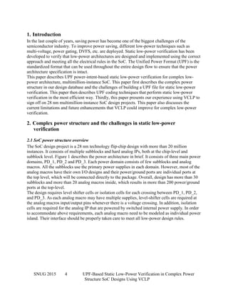
Structure SoC Designs Using VCLP
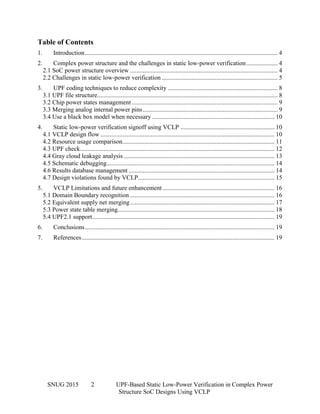
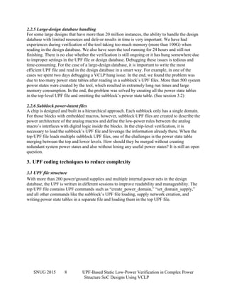
4.4 Gray cloud leakage analysis
The gray cloud leakage analysis feature is very useful in identifying issues in the timing ECOs
where buffers are inserted in the third domain. For those buffers/inverters that are placed in a
switched-power domain, the original path is broken when the switched domain is off. When
enabling gray cloud analysis in VCLP, the tool will find all the buffers placed in the third domain
and report “RAIL_BUFINV_STATE” violations on them (Figure 9). With these checks, we can
route this information to the layout owner and leave it to them to place the chain of buffers in the
correct power domain in time and without involving low-power-aware Formality. Here are
violations caught in our design, showing that the buffer chain from “BUF_inst_1” to
“BUF_inst_4” are placed in switched domain, while both the source and sink are in the AON
domain:
Tag : RAIL_BUFINV_STATE
Description : Supply off for buffer/inverter [Instance], but sink
[LogicSink] supplies on
Violation : LP:3446
Instance : BUF_inst_4
Cell : M10S31_BUFX4
CellPin : o
EndOfChain : BUF_inst_1/o
LengthOfChain : 1
LogicSource
PinName : AON_reg_387/q
LogicSink : AON_phy_top_inst/i_standby
Figure 9: VCLP errors for buffers in third domain](https://image.slidesharecdn.com/86f46ce6-6afe-4f6c-93bd-e726da75fe49-161008132256/85/UPF-Based-Static-Low-Power-Verification-in-Complex-Power-Structure-SoC-Design-Using-VCLP-13-320.jpg)
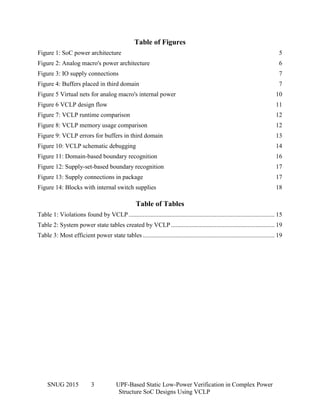
![SNUG 2015 19 UPF-Based Static Low-Power Verification in Complex Power
Structure SoC Designs Using VCLP
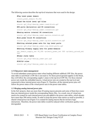
System Power States VDD block_A/Int_VDD block_B/Int_VDD
state_1 1.0 1.0 1.0
state_2 1.0 off 1.0
state_3 1.0 1.0 off
state_4 1.0 off off
Table 2: System power state tables created by VCLP
System Power States VDD block_A/Int_VDD block_B/Int_VDD
state_1 1.0 1.0 1.0
state_4 1.0 off off
Table 3: Most efficient power state tables
5.4 UPF2.1 support
UPF 2.1 (IEEE standard 1801-2013) has been released and there are a lot of new features that
could help in the static low-power verification for complex low-power design SoCs, such as low-
power strategy creation, setting equivalent nets, port attributes settings, etc. We hope VCLP can
adopt these new features in the near future, which could further improve our chip level low-
power verification process.
6.Conclusions
We have adapted to the IEEE 1801 UPF standard in our SoC design. To manage the UPF files in
this complex design, it is suggested that UPF files be written in a more modular approach.
Merging all the internal supply nets that do not have logic interactions, reading sub UPF files for
subblocks and defining power states in only top level are effective approaches to reducing UPF
complexity and run time. With the help of VCLP, we are able to identify the defects in the user-
provided UPF file at an earlier stage. It also provides a much more efficient way for static low-
power verification and debugging. Looking forward, there is still a lot work to be done in the
future. Supporting supply-set-based boundary recognition, merging supply nets, merging power
state tables and support for UPF 2.1 features are possible improvements to VCLP.
7.References
[1] Verdi Signoff-LP User Guide
[2] IEEE Standard for Design and Verification of Low-Power Integrated Circuits (Standard IEEE 1801–
2013)](https://image.slidesharecdn.com/86f46ce6-6afe-4f6c-93bd-e726da75fe49-161008132256/85/UPF-Based-Static-Low-Power-Verification-in-Complex-Power-Structure-SoC-Design-Using-VCLP-19-320.jpg)


