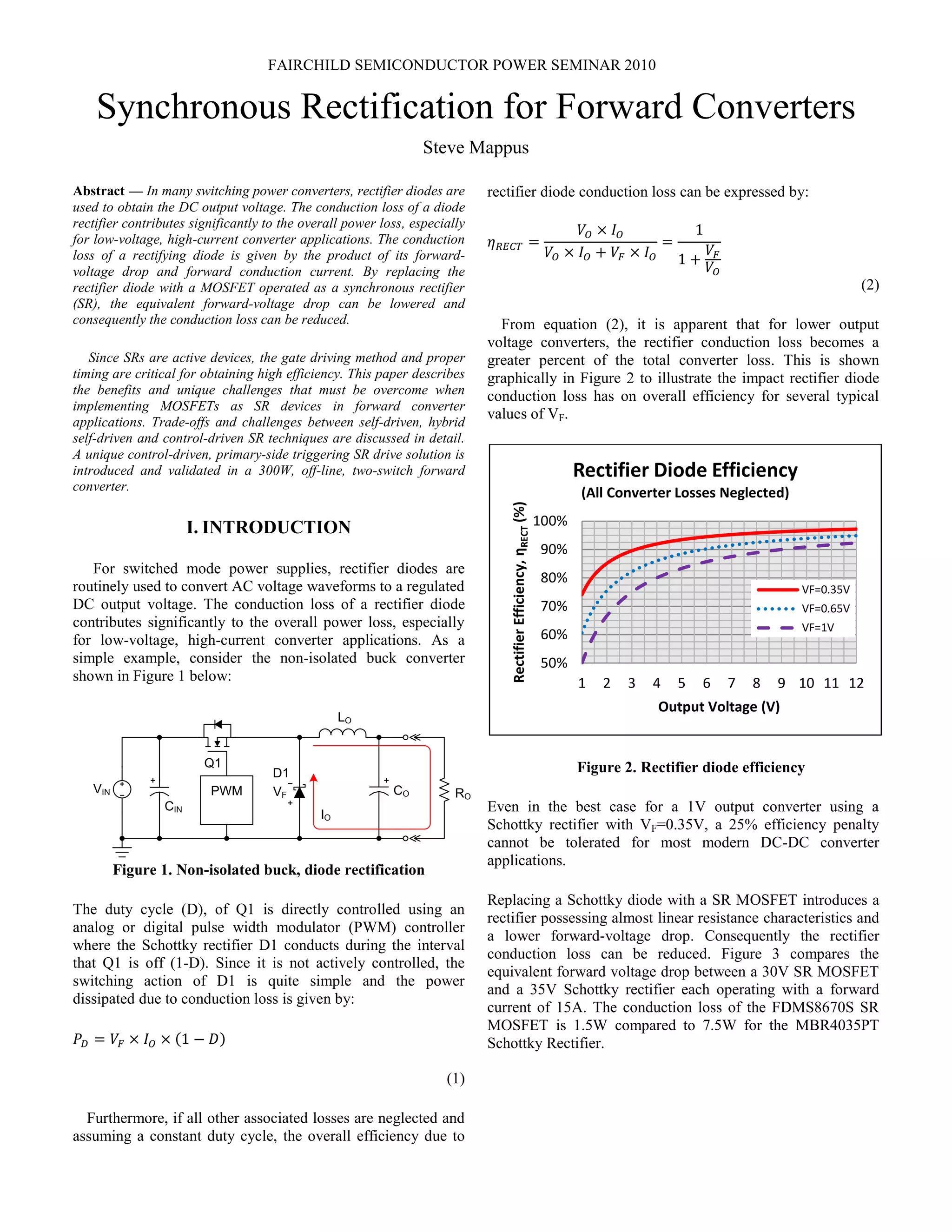
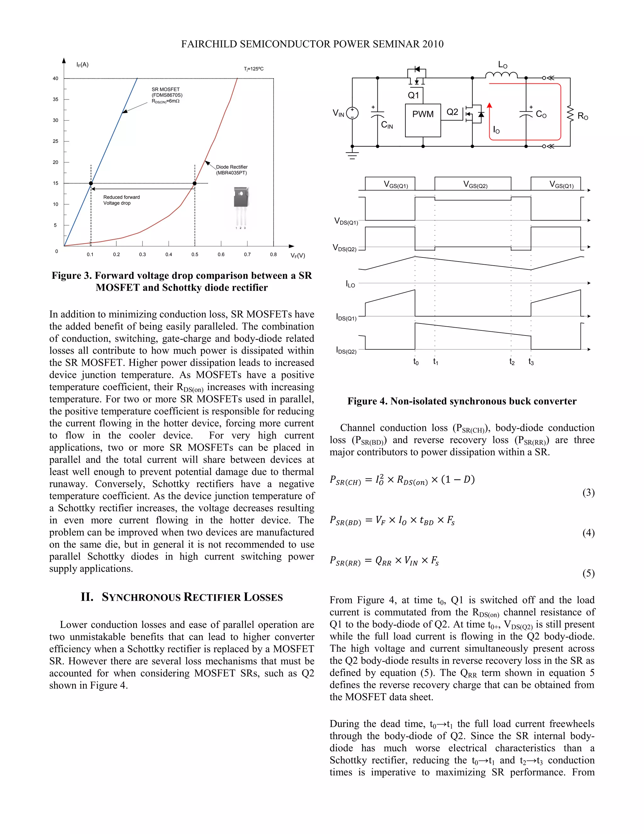
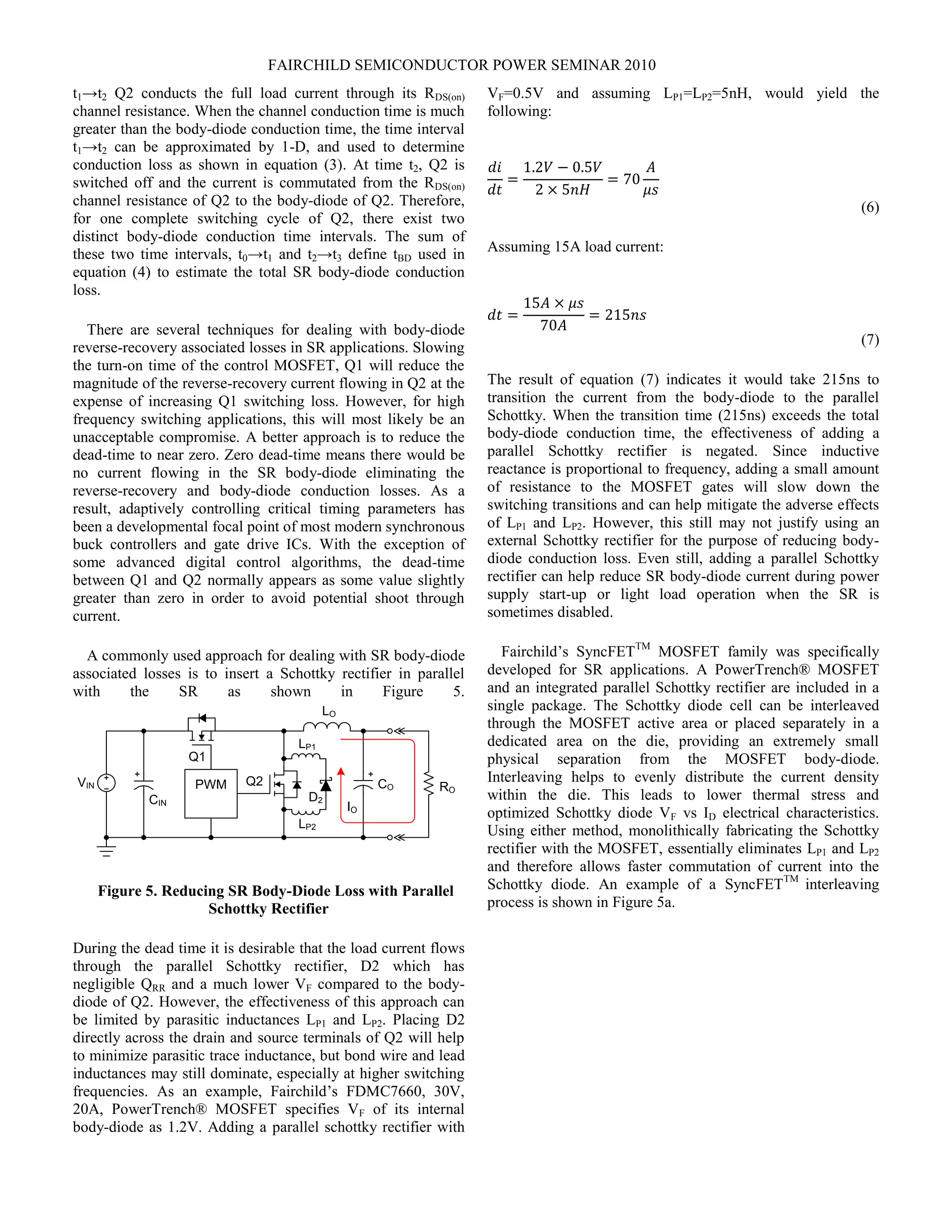
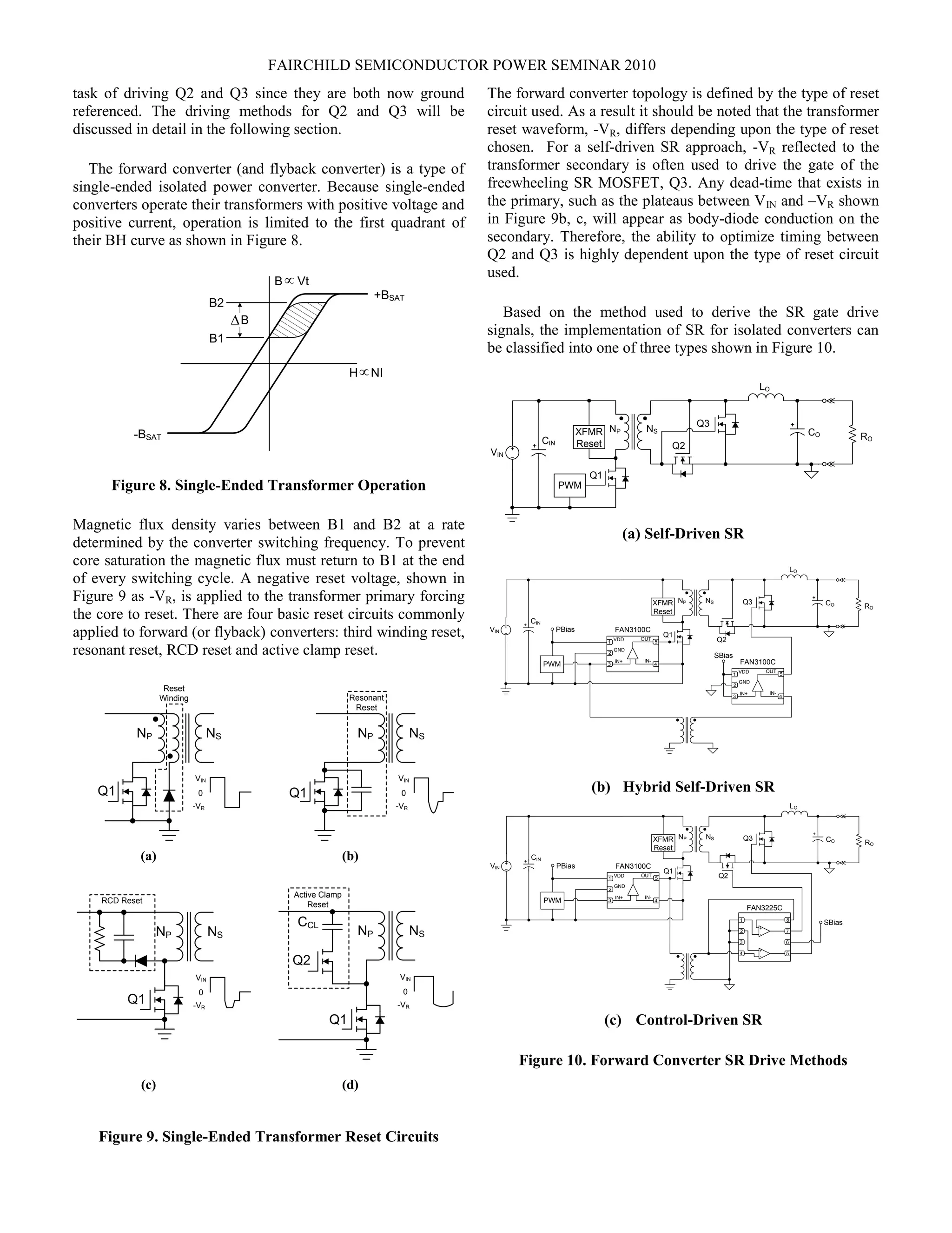
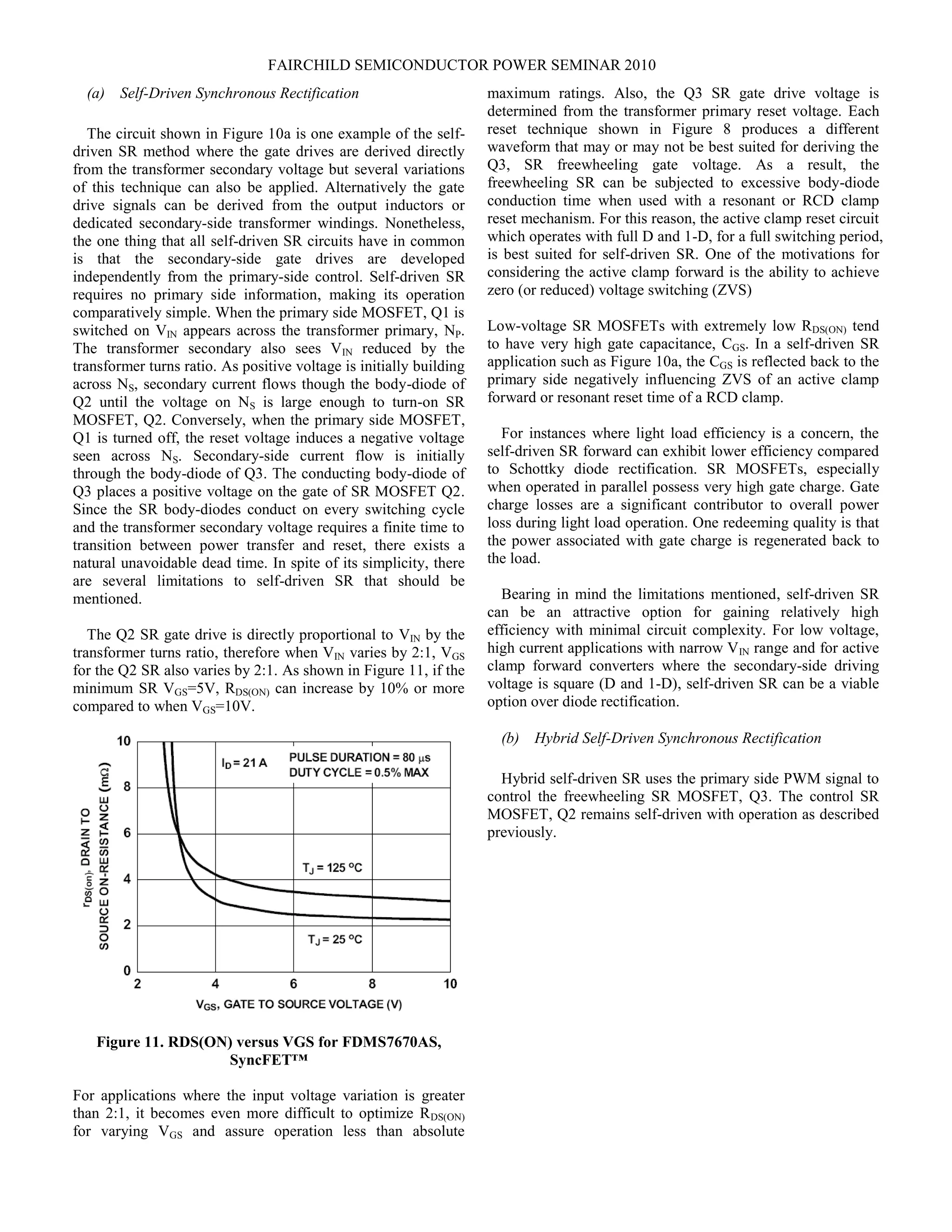
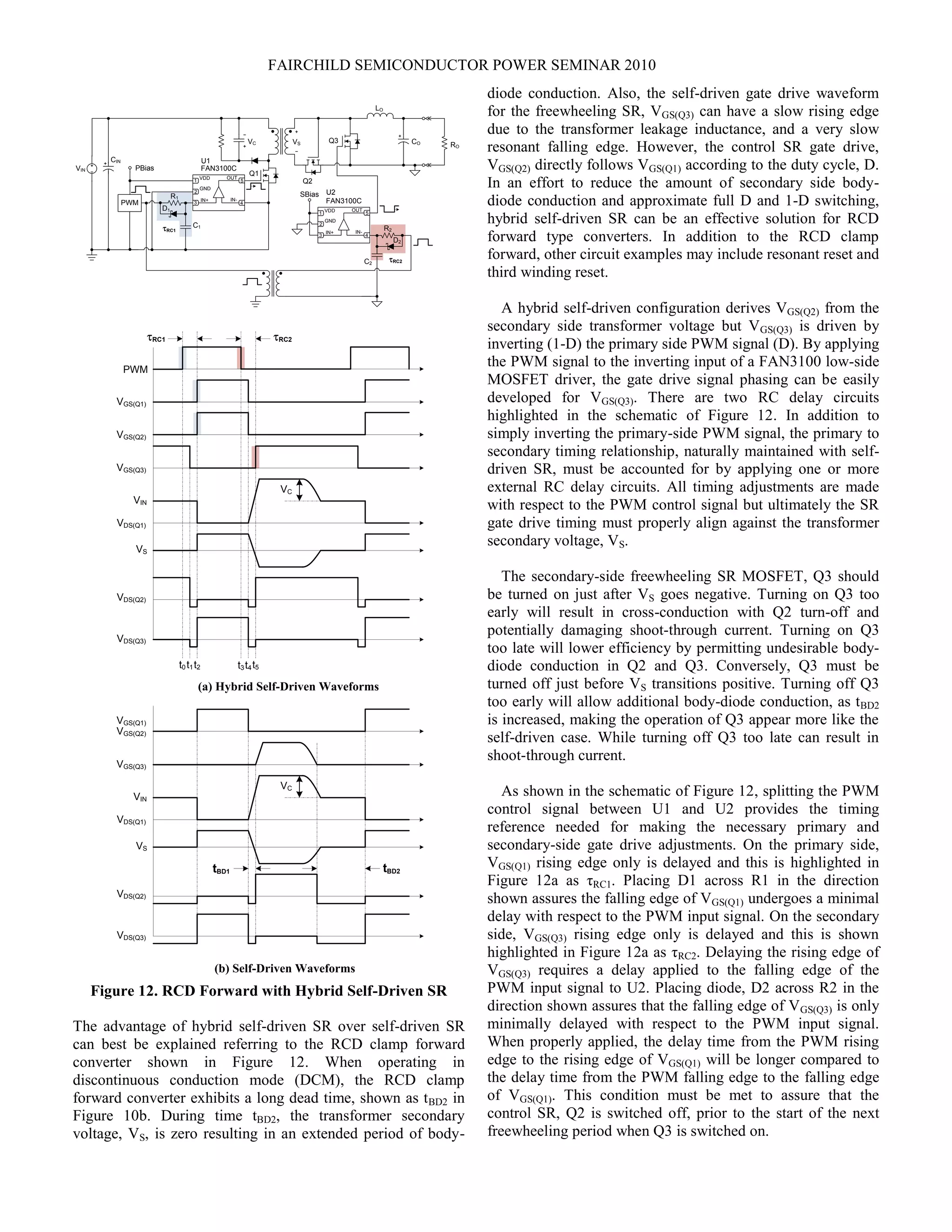
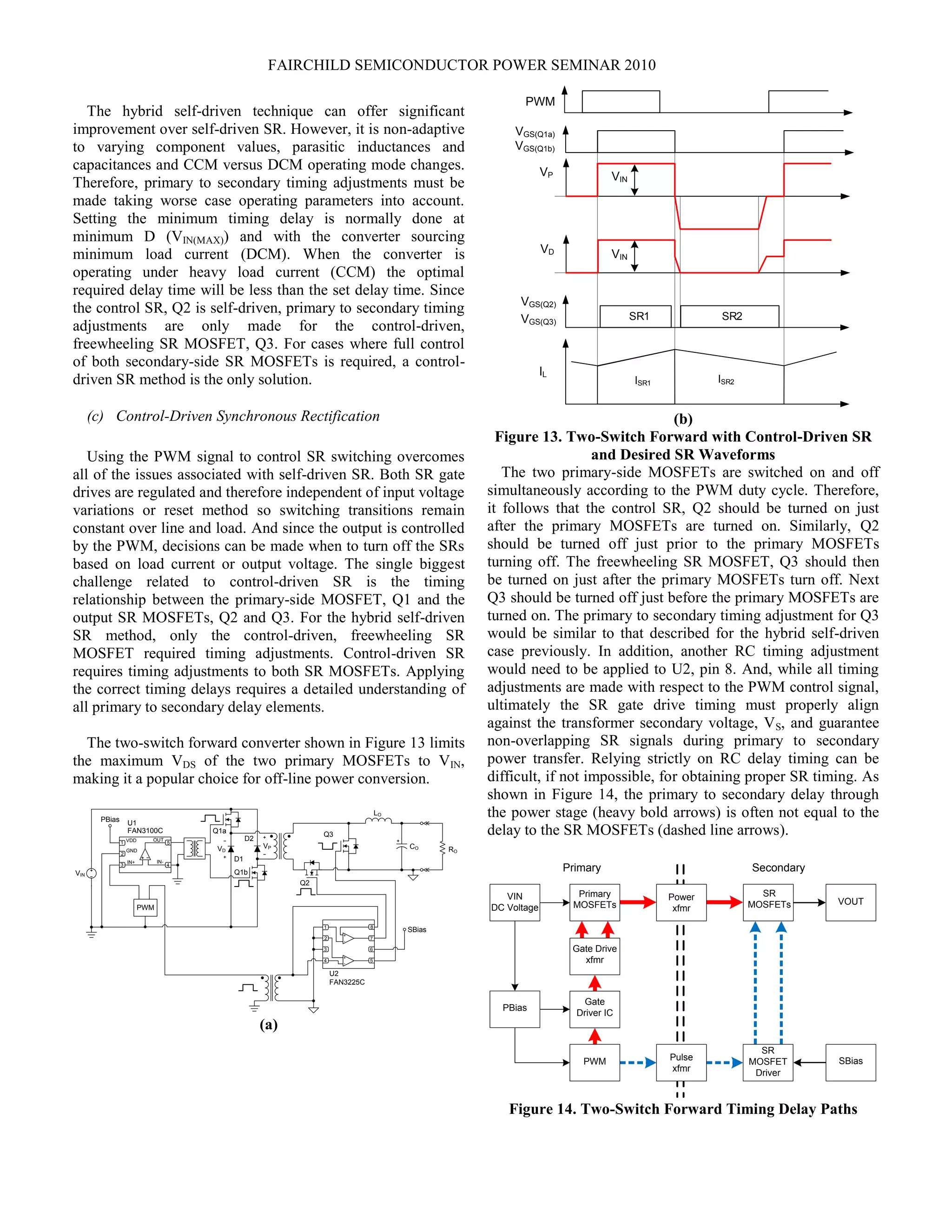
This document summarizes techniques for improving the efficiency of power converters by replacing diode rectifiers with synchronous rectifiers (SRs) using MOSFETs. SRs can reduce conduction losses by lowering the equivalent forward voltage drop compared to diodes. However, SRs introduce additional losses related to their body diode and switching operation that must be minimized through proper gate driving and timing. Integrating a Schottky diode with the SR MOSFET in a single package helps reduce body diode losses and reverse recovery effects. Optimizing the gate driving method and timing is critical for SR performance in forward converters.
This comprehensive text on Network Analysis and Synthesis is designed for undergraduate students of Electronics and Communication Engineering, Electrical and Electronics Engineering, Electronics and Instrumentation Engineering, Electronics and Computer Engineering and Biomedical Engineering. The book will also be useful to AMIE and IETE students. Buy Now: https://bit.ly/2WmA7is
Operational amplifier: inverting and non-inverting amplifier, Power bandwidth, slew rate: slew rate distortion, noise gain, band width product. cascade amplifiers- bandwidth, CMRR, PSRR, Open loop op amp characteristics.
https://www.linkedin.com/in/preeti-choudhary-266414182/
https://www.instagram.com/chaudharypreeti1997/
https://www.facebook.com/profile.php?id=100013419194533
https://twitter.com/preetic27018281
Please like, share, comment and follow.
stay connected
If any query then contact:
chaudharypreeti1997@gmail.com
Thanking-You
Preeti Choudhary
A silicon controlled rectifier or semiconductor controlled rectifier is a four-layer solid-state current-controlling device. The principle of four-layer pโnโpโn switching was developed by Moll, Tanenbaum, Goldey and Holonyak of Bell Laboratories in 1956.
For more notes on basics of electronics will see on https://www.slideshare.net/ATHEENAMILAGIPANDIAN/edit_my_uploads
The complete list of thyristor family members include diac (bidirectional diode thyristor), triac (bidirectional triode thyristor), SCR (silicon controlled rectifier), Shockley diode, SCS (silicon controlled switch), SBS (silicon bilateral switch), SUS (silicon unilateral switch) also known as comยญplementary SCR or CSCR, LASCR (light activated SCR), LAS (light activated switch) and LASCS (light activated SCS).
These are the basics of Linear circuit analysis that will help you to strong your basics in this subject.Guideline for this book is 'Electric Circuits, by Nilsson & Riedel 2009'.
Hope this will help you.
A DC-DC converter topology is presented
combining the soft switching effects of the Snubber Assisted Zero
Voltage and Zero Current Transition (SAZZ) topology and the
increased inductor frequency of the dual interleaved boost
converter with interphase transformer. The snubber capacitors
and output capacitances of the main devices are discharged prior
to turn on using a single auxiliary inductor, eliminating turn on
losses. Furthermore, the turn off losses are significantly reduced
since the energy stored in the device output capacitance at turn
off is recovered at turn on. The effectiveness of the topology is
demonstrated on a SiC prototype operating at 12.5 kW, 112 kHz,
reducing the switching losses by 50%.
The Analysis of Dead Time on Switching Loss in High and Low Side MOSFETs of Z...IDES Editor
ย
This work is about the analysis of dead time
variation on switching losses in a Zero Voltage Switching
(ZVS) synchronous buck converter (SBC) circuit. In high
frequency converter circuits, switching losses are
commonly linked with high and low side switches of SBC
circuit. They are activated externally by the gate driver
circuit. The duty ratio, dead time and resonant inductor
are the parameters that affect the efficiency of the circuit.
These variables can be adjusted for the optimization
purposes. The study primarily focuses on varying the
settings of input pulses of the MOSFETs in the resonant
gate driver circuit which consequently affects the
performance of the ZVS synchronous buck converter
circuit. Using the predetermined inductor of 9 nH, the
frequency is maintained at 1 MHz for each cycle
transition. The switching loss graph is obtained and
switching losses for both S1 and S2 are calculated and
compared to the findings from previous work. It has
shown a decrease in losses by 13.8 % in S1. A dead time of
15 ns has been determined to be optimized value in the
SBC design.
This paper addresses a novel approach for designing and modeling of the isolated
flyback converter. Modeling is done without parasitic as well as with parasitic components.
A detailed analysis, simulation and different control strategy are conferred for flyback
converter in continuous conduction mode (CCM). To verify the design and modeling at
primary stage, study of the converter is practiced in CCM operation for input AC voltage
230V at 50Hz and output DC voltage of 5V and 50W output power rating using PSIM 6.0
software. Simulation result shows a little ripple in output of the converter in open loop. Finally
in order to evaluate the system as well as response of the controller, flyback converter is
simulated using MATLAB. This work, highlighting the modeling when the system have
transformer and facilitate designers to go for it when they need one or more than one output
for a given application upto 150W
A Novel Approach of Position Estimation and Power Factor Corrector Converter ...IJPEDS-IAES
ย
This paper proposes a Power factor Corrected (PFC) Bridgeless Buck-Boost converter fed BLDC motor drive. The Bridgeless configuration eliminates the Diode Bridge Rectifier in order to reduce the number of components and the conduction loss. The position sensors used in BLDC drives have drawbacks of additional cost, mechanical alignment problems. These bottle necks results in sensorless technique. The Sensorless technique mostly relies on measurement of Back EMF to determine relative positions of stator and rotor for the correct coil energising sequence can be implemented. This paper introduces the offline Finite Element method for sensorless operation. The proposed sensorless scheme estimates the motor position at standstill and running condition. The obtained Power Factor is within the acceptable limits IEC 61000-3-2. The proposed drive is simulated in MATLAB/Simulink the obtained results are validated experimentally on a developed prototype of the drive.
Soft Switched Multi-Output Flyback Converter with Voltage DoublerIJPEDS-IAES
ย
A novel multi-output voltage doubler circuit with resonant switching
technique is proposed in this paper. The resonant topology in the primary
side of the flyback transformer switches the device either at zero voltage or
current thus optimizing the switching devices by mitigating the losses. The
voltage doubler circuit introduced in the load side increases the voltage by
twice the value thereby increasing the load power and density. The proposed
Multi-output Isolated Converter removes the need for mutiple SMPS units
for a particular application. This reduces the size and weight of the
converters considerably leading to a greater payload. This paper aims at
optimizing the proposed converter with some design changes. The results
obtained from the hardware prototype are given in a comprehensive manner
for a 3.5W converter operating at output voltages of 5V and 3.3V at 50 kHz
switching frequency. The converter output is regulated with the PI controller
designed with SG3523 IC. The effects of load and line regulation for ยฑ20%
variations are analyzed in detail.
Enhancing the Design of VRM for Testing Magnetic ComponentsIJERA Editor
ย
The aim of this work is to design, build and test a voltage regulator module circuit (VRM) that can be used to
compare the performance of different magnetic component designs. The VRM will be used to convert the input
voltage (typically 12V) to a lower level which will supply a microprocessor load e.g. the Intel Pentium. The
work will include review of VRM circuit topologies for VRM 10.1 specification. Circuit design will be
performed for available controller IC. Simulation and analysis of the circuit in PSPICE and characterization
under transient conditions, a circuit will be designed for simulating a transient load change in PSPICE.
Finally all required components will be ordered and the circuit will be built and can be used for testing of
inductors and transformers
This paper presents a new single switched inductor-capacitor coupled transformer-less high gain DC-DC converter which can be used in renewable energy sources like PV, fuelcell in which the low DC output voltage is to be converted into high dc output voltage. With the varying low input voltages, the output of DC-DC converter remains same and does not change. A state space model of the converter is also presented in the paper. This constant output voltage is obtained by close loop control of converter using PID controller. High voltage gain of 10 is obtained without use of transformer. All the simulations are done in MATLAB-SIMULINK environment.
Similar to Synchronous Rectification for Forward Converters_SMappus_June 4 2010 (20)
Synchronous Rectification for Forward Converters_SMappus_June 4 2010
1. FAIRCHILD SEMICONDUCTOR POWER SEMINAR 2010
Synchronous Rectification for Forward Converters
Steve Mappus
Abstract โ In many switching power converters, rectifier diodes are
used to obtain the DC output voltage. The conduction loss of a diode
rectifier contributes significantly to the overall power loss, especially
for low-voltage, high-current converter applications. The conduction
loss of a rectifying diode is given by the product of its forward-
voltage drop and forward conduction current. By replacing the
rectifier diode with a MOSFET operated as a synchronous rectifier
(SR), the equivalent forward-voltage drop can be lowered and
consequently the conduction loss can be reduced.
Since SRs are active devices, the gate driving method and proper
timing are critical for obtaining high efficiency. This paper describes
the benefits and unique challenges that must be overcome when
implementing MOSFETs as SR devices in forward converter
applications. Trade-offs and challenges between self-driven, hybrid
self-driven and control-driven SR techniques are discussed in detail.
A unique control-driven, primary-side triggering SR drive solution is
introduced and validated in a 300W, off-line, two-switch forward
converter.
I. INTRODUCTION
For switched mode power supplies, rectifier diodes are
routinely used to convert AC voltage waveforms to a regulated
DC output voltage. The conduction loss of a rectifier diode
contributes significantly to the overall power loss, especially
for low-voltage, high-current converter applications. As a
simple example, consider the non-isolated buck converter
shown in Figure 1 below:
D1
LO
CO
Q1
CIN
VF RO
IO
VIN PWM
Figure 1. Non-isolated buck, diode rectification
The duty cycle (D), of Q1 is directly controlled using an
analog or digital pulse width modulator (PWM) controller
where the Schottky rectifier D1 conducts during the interval
that Q1 is off (1-D). Since it is not actively controlled, the
switching action of D1 is quite simple and the power
dissipated due to conduction loss is given by:
๐๐ท = ๐๐น ร ๐ผ ๐ ร (1 โ ๐ท)
(1)
Furthermore, if all other associated losses are neglected and
assuming a constant duty cycle, the overall efficiency due to
rectifier diode conduction loss can be expressed by:
๐ ๐ ๐ธ๐ถ๐ =
๐๐ ร ๐ผ ๐
๐๐ ร ๐ผ ๐ + ๐๐น ร ๐ผ ๐
=
1
1 +
๐๐น
๐๐
(2)
From equation (2), it is apparent that for lower output
voltage converters, the rectifier conduction loss becomes a
greater percent of the total converter loss. This is shown
graphically in Figure 2 to illustrate the impact rectifier diode
conduction loss has on overall efficiency for several typical
values of VF.
Figure 2. Rectifier diode efficiency
Even in the best case for a 1V output converter using a
Schottky rectifier with VF=0.35V, a 25% efficiency penalty
cannot be tolerated for most modern DC-DC converter
applications.
Replacing a Schottky diode with a SR MOSFET introduces a
rectifier possessing almost linear resistance characteristics and
a lower forward-voltage drop. Consequently the rectifier
conduction loss can be reduced. Figure 3 compares the
equivalent forward voltage drop between a 30V SR MOSFET
and a 35V Schottky rectifier each operating with a forward
current of 15A. The conduction loss of the FDMS8670S SR
MOSFET is 1.5W compared to 7.5W for the MBR4035PT
Schottky Rectifier.
50%
60%
70%
80%
90%
100%
1 2 3 4 5 6 7 8 9 10 11 12
RectifierEfficiency,ฮทRECT(%)
Output Voltage (V)
Rectifier Diode Efficiency
(All Converter Losses Neglected)
VF=0.35V
VF=0.65V
VF=1V
2. FAIRCHILD SEMICONDUCTOR POWER SEMINAR 2010
0.1
5
10
15
20
25
Diode Rectifier
(MBR4035PT)
30
35
40
Reduced forward
Voltage drop
SR MOSFET
(FDMS8670S)
RDS(ON)=6mW
IF(A)
VF(V)0.2 0.3 0.4 0.5 0.6 0.7 0.8
Tj=125โฐC
0
Figure 3. Forward voltage drop comparison between a SR
MOSFET and Schottky diode rectifier
In addition to minimizing conduction loss, SR MOSFETs have
the added benefit of being easily paralleled. The combination
of conduction, switching, gate-charge and body-diode related
losses all contribute to how much power is dissipated within
the SR MOSFET. Higher power dissipation leads to increased
device junction temperature. As MOSFETs have a positive
temperature coefficient, their RDS(on) increases with increasing
temperature. For two or more SR MOSFETs used in parallel,
the positive temperature coefficient is responsible for reducing
the current flowing in the hotter device, forcing more current
to flow in the cooler device. For very high current
applications, two or more SR MOSFETs can be placed in
parallel and the total current will share between devices at
least well enough to prevent potential damage due to thermal
runaway. Conversely, Schottky rectifiers have a negative
temperature coefficient. As the device junction temperature of
a Schottky rectifier increases, the voltage decreases resulting
in even more current flowing in the hotter device. The
problem can be improved when two devices are manufactured
on the same die, but in general it is not recommended to use
parallel Schottky diodes in high current switching power
supply applications.
II. SYNCHRONOUS RECTIFIER LOSSES
Lower conduction losses and ease of parallel operation are
two unmistakable benefits that can lead to higher converter
efficiency when a Schottky rectifier is replaced by a MOSFET
SR. However there are several loss mechanisms that must be
accounted for when considering MOSFET SRs, such as Q2
shown in Figure 4.
LO
CO
Q1
CIN
RO
IO
VIN PWM Q2
VGS(Q1) VGS(Q2)
VDS(Q2)
VDS(Q1)
VGS(Q1)
ILO
IDS(Q1)
IDS(Q2)
t0 t1 t2 t3
Figure 4. Non-isolated synchronous buck converter
Channel conduction loss (PSR(CH)), body-diode conduction
loss (PSR(BD)) and reverse recovery loss (PSR(RR)) are three
major contributors to power dissipation within a SR.
๐ ๐๐ (๐ถ๐ป) = ๐ผ ๐
2
ร ๐ ๐ท๐(๐๐) ร (1 โ ๐ท)
(3)
๐ ๐๐ (๐ต๐ท) = ๐๐น ร ๐ผ ๐ ร ๐ก ๐ต๐ท ร ๐น๐
(4)
๐ ๐๐ (๐ ๐ ) = ๐ ๐ ๐ ร ๐๐ผ๐ ร ๐น๐
(5)
From Figure 4, at time t0, Q1 is switched off and the load
current is commutated from the RDS(on) channel resistance of
Q1 to the body-diode of Q2. At time t0+, VDS(Q2) is still present
while the full load current is flowing in the Q2 body-diode.
The high voltage and current simultaneously present across
the Q2 body-diode results in reverse recovery loss in the SR as
defined by equation (5). The QRR term shown in equation 5
defines the reverse recovery charge that can be obtained from
the MOSFET data sheet.
During the dead time, t0โt1 the full load current freewheels
through the body-diode of Q2. Since the SR internal body-
diode has much worse electrical characteristics than a
Schottky rectifier, reducing the t0โt1 and t2โt3 conduction
times is imperative to maximizing SR performance. From
3. FAIRCHILD SEMICONDUCTOR POWER SEMINAR 2010
t1โt2 Q2 conducts the full load current through its RDS(on)
channel resistance. When the channel conduction time is much
greater than the body-diode conduction time, the time interval
t1โt2 can be approximated by 1-D, and used to determine
conduction loss as shown in equation (3). At time t2, Q2 is
switched off and the current is commutated from the RDS(on)
channel resistance of Q2 to the body-diode of Q2. Therefore,
for one complete switching cycle of Q2, there exist two
distinct body-diode conduction time intervals. The sum of
these two time intervals, t0โt1 and t2โt3 define tBD used in
equation (4) to estimate the total SR body-diode conduction
loss.
There are several techniques for dealing with body-diode
reverse-recovery associated losses in SR applications. Slowing
the turn-on time of the control MOSFET, Q1 will reduce the
magnitude of the reverse-recovery current flowing in Q2 at the
expense of increasing Q1 switching loss. However, for high
frequency switching applications, this will most likely be an
unacceptable compromise. A better approach is to reduce the
dead-time to near zero. Zero dead-time means there would be
no current flowing in the SR body-diode eliminating the
reverse-recovery and body-diode conduction losses. As a
result, adaptively controlling critical timing parameters has
been a developmental focal point of most modern synchronous
buck controllers and gate drive ICs. With the exception of
some advanced digital control algorithms, the dead-time
between Q1 and Q2 normally appears as some value slightly
greater than zero in order to avoid potential shoot through
current.
A commonly used approach for dealing with SR body-diode
associated losses is to insert a Schottky rectifier in parallel
with the SR as shown in Figure 5.
LO
CO
Q1
CIN
RO
IO
VIN PWM Q2
LP1
LP2
D2
Figure 5. Reducing SR Body-Diode Loss with Parallel
Schottky Rectifier
During the dead time it is desirable that the load current flows
through the parallel Schottky rectifier, D2 which has
negligible QRR and a much lower VF compared to the body-
diode of Q2. However, the effectiveness of this approach can
be limited by parasitic inductances LP1 and LP2. Placing D2
directly across the drain and source terminals of Q2 will help
to minimize parasitic trace inductance, but bond wire and lead
inductances may still dominate, especially at higher switching
frequencies. As an example, Fairchildโs FDMC7660, 30V,
20A, PowerTrenchยฎ MOSFET specifies VF of its internal
body-diode as 1.2V. Adding a parallel schottky rectifier with
VF=0.5V and assuming LP1=LP2=5nH, would yield the
following:
๐๐
๐๐ก
=
1.2๐ โ 0.5๐
2 ร 5๐๐ป
= 70
๐ด
๐๐
(6)
Assuming 15A load current:
๐๐ก =
15๐ด ร ๐๐
70๐ด
= 215๐๐
(7)
The result of equation (7) indicates it would take 215ns to
transition the current from the body-diode to the parallel
Schottky. When the transition time (215ns) exceeds the total
body-diode conduction time, the effectiveness of adding a
parallel Schottky rectifier is negated. Since inductive
reactance is proportional to frequency, adding a small amount
of resistance to the MOSFET gates will slow down the
switching transitions and can help mitigate the adverse effects
of LP1 and LP2. However, this still may not justify using an
external Schottky rectifier for the purpose of reducing body-
diode conduction loss. Even still, adding a parallel Schottky
rectifier can help reduce SR body-diode current during power
supply start-up or light load operation when the SR is
sometimes disabled.
Fairchildโs SyncFETTM
MOSFET family was specifically
developed for SR applications. A PowerTrenchยฎ MOSFET
and an integrated parallel Schottky rectifier are included in a
single package. The Schottky diode cell can be interleaved
through the MOSFET active area or placed separately in a
dedicated area on the die, providing an extremely small
physical separation from the MOSFET body-diode.
Interleaving helps to evenly distribute the current density
within the die. This leads to lower thermal stress and
optimized Schottky diode VF vs ID electrical characteristics.
Using either method, monolithically fabricating the Schottky
rectifier with the MOSFET, essentially eliminates LP1 and LP2
and therefore allows faster commutation of current into the
Schottky diode. An example of a SyncFETTM
interleaving
process is shown in Figure 5a.
4. FAIRCHILD SEMICONDUCTOR POWER SEMINAR 2010
Trench MOS
SyncFETโข
Schottky
Figure 5a. SyncFETโข Monolithic Fabrication
As mentioned previously, a Schottky rectifier generally has a
QRR lower than that of an intrinsic body-diode. The reverse-
recovery current waveforms shown in Figure 6 compare a
FDMS7670S SyncFETโข to a similar sized, FDMS7670 non-
SyncFETโข die. The reverse-recovery charge, QRR is
determined from the measured source-drain current (Isd) and
reverse-recovery time (tRR) and results in a QRR improvement
of 10%. The higher channel density and deeper cell trench
used in Fairchildโs low-voltage process yields an intrinsic
body-diode possessing reverse-recovery characteristics more
closely matched to a Schottky rectifier. SyncFETโข
comparisons made using previous generation standard trench
technology would yield QRR improvements closer to 50% for
example. Also, because the Schottky is integrated with the
MOSFET, its forward voltage drop is much lower than the
voltage drop across the intrinsic body-diode, 0.43V compared
to 0.7V. This results in substantially less power loss during the
dead-time in a synchronous buck converter application.
FIGURE 6
-4
-2
0
2
4
6
0 10 20 30 40 50
Isd(A)
time (ns)
Measured QRR
20A,300A/ยตs
FDMS7670
FDMS7670S
DQRR~10%
Figure 6. Measured Reverse Recovery Waveforms for
SyncFETโข vs Non-SyncFETโข
Because SRs are active devices, their ability to outperform a
Schottky diode rectifier is highly dependent upon the gate
driving method used and timing with respect to the PWM
controlled MOSFET. A summary of performance
characteristics important for driving SRs in non-isolated
synchronous buck converters would include:
1. Anti-cross conduction protection to assure that the
two MOSFETs, Q1 and Q2 never actively conduct
at the same time.
2. Minimizing the dead time between Q1 and Q2 to
reduce frequency related power losses associated
with SR MOSFET body-diode conduction and
reverse-recovery time.
3. Peak gate drive current optimized to efficiently
overcome the high-gate charge associated with low
on-resistance SR MOSFETs.
4. The SR gate drive should include a very low
impedance pull-down to assure the gate is held low
when high dv/dt is applied across the drain-source
terminals.
For non-isolated synchronous buck converters, most of the
issues associated with driving the SR MOSFET are covered
by features incorporated in numerous PWM controllers and
gate driver ICs dedicated to this very popular converter
topology. The interface between the PWM controller and
the power stage is direct. The controller or gate drive IC can
easily sense the current in any leg or the voltage at any node
and use this information for making decisions regarding
proper gate drive timing. For isolated buck derived
converters, the introduction of a power transformer adds an
entire new set of SR challenges in addition to many of the
same concerns related to the non-isolated synchronous buck.
III. FORWARD CONVERTER SR CONSIDERATIONS
The forward converter is sometimes referred to as an
isolated buck converter from the standpoint that the secondary
side includes two rectifiers used in a high-side, low-side
configuration. Similar to a non-isolated synchronous buck
converter, the two output SRs feed a LC filter, except that a
power transformer isolates the input voltage from the
regulated DC output voltage. Because Q2 is in series with the
transformer secondary it can be moved from the high-side to
the low-side as highlighted in Figure 7.
ISOLATED
SYNCHRONOUS BUCK
Q2
LO
CO
NP NS
CIN
Q1
RO
VIN
XFMR
Reset
PWM
Q3
VR
Figure 7. Forward Converter with Synchronous Rectifiers
Moving Q2 to the low-side secondary return simplifies the
5. FAIRCHILD SEMICONDUCTOR POWER SEMINAR 2010
task of driving Q2 and Q3 since they are both now ground
referenced. The driving methods for Q2 and Q3 will be
discussed in detail in the following section.
The forward converter (and flyback converter) is a type of
single-ended isolated power converter. Because single-ended
converters operate their transformers with positive voltage and
positive current, operation is limited to the first quadrant of
their BH curve as shown in Figure 8.
๏ตB Vt
๏ตH NI
DB
B1
B2
+BSAT
-BSAT
Figure 8. Single-Ended Transformer Operation
Magnetic flux density varies between B1 and B2 at a rate
determined by the converter switching frequency. To prevent
core saturation the magnetic flux must return to B1 at the end
of every switching cycle. A negative reset voltage, shown in
Figure 9 as -VR, is applied to the transformer primary forcing
the core to reset. There are four basic reset circuits commonly
applied to forward (or flyback) converters: third winding reset,
resonant reset, RCD reset and active clamp reset.
NP NS
Q1
RCD Reset
NP NS
Q1
Resonant
Reset
Q2
CCL
NP NS
Q1
Active Clamp
Reset
NP NS
Q1
Reset
Winding
(a) (b)
(c) (d)
0
VIN
-VR
0
VIN
-VR
0
VIN
-VR
0
VIN
-VR
Figure 9. Single-Ended Transformer Reset Circuits
The forward converter topology is defined by the type of reset
circuit used. As a result it should be noted that the transformer
reset waveform, -VR, differs depending upon the type of reset
chosen. For a self-driven SR approach, -VR reflected to the
transformer secondary is often used to drive the gate of the
freewheeling SR MOSFET, Q3. Any dead-time that exists in
the primary, such as the plateaus between VIN and โVR shown
in Figure 9b, c, will appear as body-diode conduction on the
secondary. Therefore, the ability to optimize timing between
Q2 and Q3 is highly dependent upon the type of reset circuit
used.
Based on the method used to derive the SR gate drive
signals, the implementation of SR for isolated converters can
be classified into one of three types shown in Figure 10.
Q2
LO
CO
NP NS
CIN
Q1
RO
VIN
XFMR
Reset
PWM
Q3
(a) Self-Driven SR
Q2
LO
CO
NP NS
CIN
Q1
RO
VIN
XFMR
Reset
Q3
1
2
3 4
5VDD
GND
IN-IN+
FAN3100C
OUT
SBias
PWM
1
2
3 4
5VDD
GND
IN-IN+
FAN3100C
OUT
PBias
(b) Hybrid Self-Driven SR
Q2
LO
CO
NP NS
CIN
Q1
RO
VIN
XFMR
Reset
Q3
SBias
PWM
1
2
3 4
5VDD
GND
IN-IN+
FAN3100C
OUT
PBias
1
2
3 6
8
FAN3225C
7
4 5
+
-
+
-
(c) Control-Driven SR
Figure 10. Forward Converter SR Drive Methods
6. FAIRCHILD SEMICONDUCTOR POWER SEMINAR 2010
(a) Self-Driven Synchronous Rectification
The circuit shown in Figure 10a is one example of the self-
driven SR method where the gate drives are derived directly
from the transformer secondary voltage but several variations
of this technique can also be applied. Alternatively the gate
drive signals can be derived from the output inductors or
dedicated secondary-side transformer windings. Nonetheless,
the one thing that all self-driven SR circuits have in common
is that the secondary-side gate drives are developed
independently from the primary-side control. Self-driven SR
requires no primary side information, making its operation
comparatively simple. When the primary side MOSFET, Q1 is
switched on VIN appears across the transformer primary, NP.
The transformer secondary also sees VIN reduced by the
transformer turns ratio. As positive voltage is initially building
across NS, secondary current flows though the body-diode of
Q2 until the voltage on NS is large enough to turn-on SR
MOSFET, Q2. Conversely, when the primary side MOSFET,
Q1 is turned off, the reset voltage induces a negative voltage
seen across NS. Secondary-side current flow is initially
through the body-diode of Q3. The conducting body-diode of
Q3 places a positive voltage on the gate of SR MOSFET Q2.
Since the SR body-diodes conduct on every switching cycle
and the transformer secondary voltage requires a finite time to
transition between power transfer and reset, there exists a
natural unavoidable dead time. In spite of its simplicity, there
are several limitations to self-driven SR that should be
mentioned.
The Q2 SR gate drive is directly proportional to VIN by the
transformer turns ratio, therefore when VIN varies by 2:1, VGS
for the Q2 SR also varies by 2:1. As shown in Figure 11, if the
minimum SR VGS=5V, RDS(ON) can increase by 10% or more
compared to when VGS=10V.
Figure 11. RDS(ON) versus VGS for FDMS7670AS,
SyncFETโข
For applications where the input voltage variation is greater
than 2:1, it becomes even more difficult to optimize RDS(ON)
for varying VGS and assure operation less than absolute
maximum ratings. Also, the Q3 SR gate drive voltage is
determined from the transformer primary reset voltage. Each
reset technique shown in Figure 8 produces a different
waveform that may or may not be best suited for deriving the
Q3, SR freewheeling gate voltage. As a result, the
freewheeling SR can be subjected to excessive body-diode
conduction time when used with a resonant or RCD clamp
reset mechanism. For this reason, the active clamp reset circuit
which operates with full D and 1-D, for a full switching period,
is best suited for self-driven SR. One of the motivations for
considering the active clamp forward is the ability to achieve
zero (or reduced) voltage switching (ZVS)
Low-voltage SR MOSFETs with extremely low RDS(ON) tend
to have very high gate capacitance, CGS. In a self-driven SR
application such as Figure 10a, the CGS is reflected back to the
primary side negatively influencing ZVS of an active clamp
forward or resonant reset time of a RCD clamp.
For instances where light load efficiency is a concern, the
self-driven SR forward can exhibit lower efficiency compared
to Schottky diode rectification. SR MOSFETs, especially
when operated in parallel possess very high gate charge. Gate
charge losses are a significant contributor to overall power
loss during light load operation. One redeeming quality is that
the power associated with gate charge is regenerated back to
the load.
Bearing in mind the limitations mentioned, self-driven SR
can be an attractive option for gaining relatively high
efficiency with minimal circuit complexity. For low voltage,
high current applications with narrow VIN range and for active
clamp forward converters where the secondary-side driving
voltage is square (D and 1-D), self-driven SR can be a viable
option over diode rectification.
(b) Hybrid Self-Driven Synchronous Rectification
Hybrid self-driven SR uses the primary side PWM signal to
control the freewheeling SR MOSFET, Q3. The control SR
MOSFET, Q2 remains self-driven with operation as described
previously.
7. FAIRCHILD SEMICONDUCTOR POWER SEMINAR 2010
Q2
LO
CO
CIN
Q1
RO
VIN
Q3
1
2
3 4
5VDD
GND
IN-IN+
FAN3100C
OUT
SBias
PWM
1
2
3 4
5VDD
GND
IN-IN+
FAN3100C
OUT
PBias
VC VS
tRC1
tRC2
U1
U2
R1
C1
D1
C2
R2
D2
VGS(Q2)
VGS(Q3)
VDS(Q1)
VS
PWM
VGS(Q1)
VC
VIN
VDS(Q2)
VDS(Q3)
tRC1 tRC2
VGS(Q2)
VGS(Q3)
VDS(Q1)
VS
VGS(Q1)
VC
VIN
VDS(Q2)
VDS(Q3)
(a) Hybrid Self-Driven Waveforms
(b) Self-Driven Waveforms
tBD2tBD1
t0 t1t2 t3t4t5
Figure 12. RCD Forward with Hybrid Self-Driven SR
The advantage of hybrid self-driven SR over self-driven SR
can best be explained referring to the RCD clamp forward
converter shown in Figure 12. When operating in
discontinuous conduction mode (DCM), the RCD clamp
forward converter exhibits a long dead time, shown as tBD2 in
Figure 10b. During time tBD2, the transformer secondary
voltage, VS, is zero resulting in an extended period of body-
diode conduction. Also, the self-driven gate drive waveform
for the freewheeling SR, VGS(Q3) can have a slow rising edge
due to the transformer leakage inductance, and a very slow
resonant falling edge. However, the control SR gate drive,
VGS(Q2) directly follows VGS(Q1) according to the duty cycle, D.
In an effort to reduce the amount of secondary side body-
diode conduction and approximate full D and 1-D switching,
hybrid self-driven SR can be an effective solution for RCD
forward type converters. In addition to the RCD clamp
forward, other circuit examples may include resonant reset and
third winding reset.
A hybrid self-driven configuration derives VGS(Q2) from the
secondary side transformer voltage but VGS(Q3) is driven by
inverting (1-D) the primary side PWM signal (D). By applying
the PWM signal to the inverting input of a FAN3100 low-side
MOSFET driver, the gate drive signal phasing can be easily
developed for VGS(Q3). There are two RC delay circuits
highlighted in the schematic of Figure 12. In addition to
simply inverting the primary-side PWM signal, the primary to
secondary timing relationship, naturally maintained with self-
driven SR, must be accounted for by applying one or more
external RC delay circuits. All timing adjustments are made
with respect to the PWM control signal but ultimately the SR
gate drive timing must properly align against the transformer
secondary voltage, VS.
The secondary-side freewheeling SR MOSFET, Q3 should
be turned on just after VS goes negative. Turning on Q3 too
early will result in cross-conduction with Q2 turn-off and
potentially damaging shoot-through current. Turning on Q3
too late will lower efficiency by permitting undesirable body-
diode conduction in Q2 and Q3. Conversely, Q3 must be
turned off just before VS transitions positive. Turning off Q3
too early will allow additional body-diode conduction, as tBD2
is increased, making the operation of Q3 appear more like the
self-driven case. While turning off Q3 too late can result in
shoot-through current.
As shown in the schematic of Figure 12, splitting the PWM
control signal between U1 and U2 provides the timing
reference needed for making the necessary primary and
secondary-side gate drive adjustments. On the primary side,
VGS(Q1) rising edge only is delayed and this is highlighted in
Figure 12a as ฯRC1. Placing D1 across R1 in the direction
shown assures the falling edge of VGS(Q1) undergoes a minimal
delay with respect to the PWM input signal. On the secondary
side, VGS(Q3) rising edge only is delayed and this is shown
highlighted in Figure 12a as ฯRC2. Delaying the rising edge of
VGS(Q3) requires a delay applied to the falling edge of the
PWM input signal to U2. Placing diode, D2 across R2 in the
direction shown assures that the falling edge of VGS(Q3) is only
minimally delayed with respect to the PWM input signal.
When properly applied, the delay time from the PWM rising
edge to the rising edge of VGS(Q1) will be longer compared to
the delay time from the PWM falling edge to the falling edge
of VGS(Q1). This condition must be met to assure that the
control SR, Q2 is switched off, prior to the start of the next
freewheeling period when Q3 is switched on.
8. FAIRCHILD SEMICONDUCTOR POWER SEMINAR 2010
The hybrid self-driven technique can offer significant
improvement over self-driven SR. However, it is non-adaptive
to varying component values, parasitic inductances and
capacitances and CCM versus DCM operating mode changes.
Therefore, primary to secondary timing adjustments must be
made taking worse case operating parameters into account.
Setting the minimum timing delay is normally done at
minimum D (VIN(MAX)) and with the converter sourcing
minimum load current (DCM). When the converter is
operating under heavy load current (CCM) the optimal
required delay time will be less than the set delay time. Since
the control SR, Q2 is self-driven, primary to secondary timing
adjustments are only made for the control-driven,
freewheeling SR MOSFET, Q3. For cases where full control
of both secondary-side SR MOSFETs is required, a control-
driven SR method is the only solution.
(c) Control-Driven Synchronous Rectification
Using the PWM signal to control SR switching overcomes
all of the issues associated with self-driven SR. Both SR gate
drives are regulated and therefore independent of input voltage
variations or reset method so switching transitions remain
constant over line and load. And since the output is controlled
by the PWM, decisions can be made when to turn off the SRs
based on load current or output voltage. The single biggest
challenge related to control-driven SR is the timing
relationship between the primary-side MOSFET, Q1 and the
output SR MOSFETs, Q2 and Q3. For the hybrid self-driven
SR method, only the control-driven, freewheeling SR
MOSFET required timing adjustments. Control-driven SR
requires timing adjustments to both SR MOSFETs. Applying
the correct timing delays requires a detailed understanding of
all primary to secondary delay elements.
The two-switch forward converter shown in Figure 13 limits
the maximum VDS of the two primary MOSFETs to VIN,
making it a popular choice for off-line power conversion.
Q2
LO
CO RO
SBias1
2
3 6
8
U2
FAN3225C
7
4 5
+
-
+
-
VIN
PWM
1
2
3 4
5VDD
GND
IN-IN+
FAN3100C
OUT
PBias U1
Q1b
Q1a
D2
D1
Q3
VPVD
(a)
ISR1 ISR2
SR1 SR2
VGS(Q1a)
VGS(Q1b)
VP
VD
VIN
VGS(Q2)
VGS(Q3)
IL
VIN
PWM
(b)
Figure 13. Two-Switch Forward with Control-Driven SR
and Desired SR Waveforms
The two primary-side MOSFETs are switched on and off
simultaneously according to the PWM duty cycle. Therefore,
it follows that the control SR, Q2 should be turned on just
after the primary MOSFETs are turned on. Similarly, Q2
should be turned off just prior to the primary MOSFETs
turning off. The freewheeling SR MOSFET, Q3 should then
be turned on just after the primary MOSFETs turn off. Next
Q3 should be turned off just before the primary MOSFETs are
turned on. The primary to secondary timing adjustment for Q3
would be similar to that described for the hybrid self-driven
case previously. In addition, another RC timing adjustment
would need to be applied to U2, pin 8. And, while all timing
adjustments are made with respect to the PWM control signal,
ultimately the SR gate drive timing must properly align
against the transformer secondary voltage, VS, and guarantee
non-overlapping SR signals during primary to secondary
power transfer. Relying strictly on RC delay timing can be
difficult, if not impossible, for obtaining proper SR timing. As
shown in Figure 14, the primary to secondary delay through
the power stage (heavy bold arrows) is often not equal to the
delay to the SR MOSFETs (dashed line arrows).
Primary Secondary
Gate
Driver IC
Primary
MOSFETs
PBias
PWM Pulse
xfmr
Power
xfmr
VIN
DC Voltage
Gate Drive
xfmr
SR
MOSFET
Driver
SR
MOSFETs VOUT
SBias
Figure 14. Two-Switch Forward Timing Delay Paths
9. FAIRCHILD SEMICONDUCTOR POWER SEMINAR 2010
In most cases, the high voltage gate drive circuitry for the
primary MOSFETs will have a much different propagation
delay compared to the low-voltage, secondary-side SR gate
drive circuitry. The power stage delay also includes an off-line
power transformer which will have a larger propagation delay
compared to the pulse transformer used to pass the SR gate
drive signals to the secondary side. Optimizing proper SR gate
drive timing is further complicated by the fact that the PWM
can be located either on the primary (as shown in Figure 14)
or secondary-side. As a result, the task of implementing
control-driven SR often requires more accurate timing
adjustment algorithms that can be designed discretely but are
much simpler when integrated into a silicon solution.
IV. CONTROL-DRIVEN SR USING PRIMARY-SIDE
TRIGGERING
Shown in Figure 15 is a two-switch forward converter that
senses primary and secondary-side power stage information to
accurately compose secondary-side SR gate drive signals. The
FAN6210 Primary-Side SR Trigger Controller uses a single
channel PWM signal input (SIN) to generate two, edge-
triggered output signals, XP and XN. An internal fixed time
delay applied to the PWM input signal, allows the time
necessary to align the secondary-side SR MOSFET switching
transitions with the applied transformer voltage.
Q2
LO
CO
Q1b
Q1a
D2
D1
Q3
RDLY DET
XP GND
SIN
1
2
3
4
8
7
6
5
XN SOUT
VDD
SP VDD
LPC1 SR1
SN
1
2
3
4
8
7
6
5
LPC2 GND
SR2
VIN
+
FAN6210
FAN6206
LM
PWM
VO
+
R1
R2
R3 R4
DB
DZ
Figure 15. Two-Switch Forward, Primary-Side Trigger SR Control
SIN
SOUT
DET
300ns
100ns
700ns
Programmable delay
700nsXP
XN
50ns
50ns
300ns
50ns
300ns
300ns
50ns
300ns
Programmable delay
Gate drive for control SR Gate drive for Freewheeling SR
(a) Heavy Load Condition โ XP Triggered by XN
SIN
SOUT
DET
300ns
100ns
700ns
Programmable delay
700nsXP
XN
50ns
50ns
300ns
50ns
300ns
300ns
50ns
300ns
Programmable delay
Gate drive for control SR Gate drive for Freewheeling SR
(b) Light Load Condition โ XP Triggered by DET
Figure 16. FAN6210 SR Timing Diagram versus Load Current
10. FAIRCHILD SEMICONDUCTOR POWER SEMINAR 2010
As seen in the timing diagram of Figure 16, the rising edge
of XP is used to determine the turn-on time of Q2 and Q3
while the rising edge of XN is used to determine the turn-off
time of Q2 and Q3. XP and XN signals are narrow pulses
representing delayed primary-side PWM edges respectively.
XN has a 300ns pulse-width and is always triggered by the
rising and falling edge of the PWM input signal, after a 50ns
internally set delay. Corresponding to the PWM input rising
edge, XN is sent to the secondary-side where it is used to turn
off the freewheeling SR MOSFET. Only after the
freewheeling SR is turned off, can the SOUT signal be applied
to the primary side MOSFETs. The 300ns internal delay is
such that the freewheeling SR is always turned off before the
primary-side MOSFETs are turned on.
After the delayed PWM input signal (SOUT) transitions
HIGH, the XP signal is then released, commanding the turn-on
of the secondary-side SR MOSFET, Q2. The dead-time
between SOUT and XP should be minimized and is therefore
user-adjustable by a single resistor from RDLY to ground. XP
has a 700ns pulse-width and requires two conditions that must
be met for triggering:
1. The rising edge of the PWM output (SOUT) signal
and
2. XN is LOW
And,
1. The falling edge of the DET signal and
2. XN is LOW
During the PWM input turn-off, SOUT is commanded off
faster compared to the turn-on period. This can be seen in
Figure 16 by the 300ns delay applied to the SOUT turn-on
compared to the 100ns delay time applied to SOUT turn-off.
Since PWM controllers modulate the off-time (trailing edge
modulation), the delay applied to the trailing edge needs to be
as small as possible so that accurate control of the power stage
can be maintained. On the other hand, the SOUT trailing edge
delay time must be long enough such that the rising edge of
XN (triggered by SIN falling edge) occurs prior to the falling
edge of SOUT. When the primary-side PWM MOSFETs are
turned off, the transformer primary voltage begins to reverse
as the winding voltage decreases to negative VIN. During this
transformer reset period the dv/dt transition can vary as a
function of output load current. The optimum turn-on point of
the freewheeling SR MOSFET is just after the transformer
secondary winding voltage has decreased lower than VOUT.
This optimal turn-on point is determined by the DET signal
which is used to monitor the clamped primary-side
transformer winding voltage. During heavy load operation, the
dv/dt seen by the DET pin increases so it would be possible
that XP is triggered while XN is still HIGH. If XN is still
HIGH while DET has transitioned LOW, then XP is not
allowed to trigger until XN transitions LOW. Triggering XP
this way prevents SR shoot-through by ensuring that XP and
XN can never overlap. Conversely, during light load
operation, the dv/dt seen at the DET pin decreases to the point
that the DET falling edge comes after XN falls to zero.
Therefore in this case, the XP signal is triggered by the DET
voltage, after a 50ns delay time. Since the XP and XN pulses
are not the โrealโ PWM signal, they cannot be used to drive
the SR MOSFETs directly. Instead, XP and XN are used as
inputs and decoded by the FAN6206 secondary-side SR
controller and driver. The primary-side FAN6210 assumes
CCM operation for the power stage. However, during DCM
operation, the inductor current can be allowed to go negative.
Since secondary side information is not transferred to the
primary, the FAN6210 has no way to determine DCM
operation.
Under CCM operation the gate drive timing is determined
by SP (XP) and SN (XN) with operation as described by the
timing diagram of Figure 16. However, since SN is triggered
by the FAN6210 PWM input signal, the freewheeling SR
MOSFET cannot be turned off before the output inductor
current reaches zero. For DCM operation negative inductor
current would be allowed to flow in the secondary SRs.
Turning on the control SR MOSFET under this condition can
result in exceedingly high VDS ringing during DCM
operation. In the best case, this ringing might be controlled
using a dissipative RC snubber at the cost of a slight penalty in
efficiency. In the worst case, the voltage could ring high
enough to exceed the maximum breakdown voltage of the SR
MOSFET. To emulate DCM diode rectification, the
freewheeling SR MOSFET should ideally be turned off the
instant the output inductor current reaches 0A, preventing
negative current flow.
By sensing the drain-source voltage of each SR as shown in
Figure 15, FAN6206 introduces a timing control technique
called linear predict control (LPC) to accurately determine the
optimal freewheeling SR MOSFET turn-off time during DCM
operation. Figure 17 shows the LPC timing diagram relative
to the FAN6210 primary-side signals when operating in DCM.
700ns
300ns 300ns
Gate drive for
Control SR
Gate drive for Freewheeling SR
700ns
300ns
Determined by
LPC mechanism
SIN
SOUT
SP
SN
Q2
Q3
ILo
Freewheeling SR divided
drain-source voltage
LPC1
LPC2
Control SR divided drain-source voltage
tPD-LOW-SN1
Winding
detectionDET
300ns
PWM Input Signal
Gate drive output signal
50ns
tPD-HIGH-SP1
tPD-HIGH-SP2
50ns
50ns
50ns
300ns
Figure 17. FAN6206 DCM Timing Diagram
11. FAIRCHILD SEMICONDUCTOR POWER SEMINAR 2010
When operating in DCM, the current through the
freewheeling SR decreases to zero prior to the SN (XN) turn-
off command. In order to prevent negative current flow, the
drain-source voltage dividers R1, R2 for the freewheeling SR
and R3, R4 for the control SR must be properly set to sense
the voltage at the correct LPC threshold. The voltage divider
scaling for LPC1 and LPC2 is defined as:
๐น๐๐๐๐ ๐ณ๐ท๐ช๐ =
๐น๐
๐น๐ + ๐น๐
(8)
๐น๐๐๐๐ ๐ณ๐ท๐ช๐ =
๐น๐
๐น๐ + ๐น๐
(9)
LPC is not necessary for the control SR because it is always
turned off by the SN (XN) signal. Nonetheless, the control SR
voltage divider, R3, R4 is used to determine the state of the
drain-source voltage according to an internal 2V threshold
used by LPC1. LPC1 being less than 2V and SP (XP) rising
edge are the two required conditions for triggering the turn-on
of the SR1 gate drive signal. It is therefore recommended to
set the R2, R3 voltage divider within the range of 3V to 5V
according to equation (10):
3๐ < ๐ ๐๐ก๐๐๐ฟ๐๐ถ1 ร
๐ ๐ผ๐
๐
< 5๐
(10)
Where RatioLPC1 is given by equation (8), VIN is the forward
converter input voltage and n is the transformer turns ratio.
The drain-source voltage divider, RatioLPC2, plays a much
different role for the turn-off of the freewheeling SR
MOSFET. The voltage present on LPC2 is detected by an
internal voltage dependant current source, iCHG, used to charge
a fixed capacitor. However, the discharge current, iDISCHG, is
controlled by the FAN6206 bias voltage on VDD but is
constant. The value of iCHG results in an applied dv/dt which is
used to precisely determine the turn-off timing for the
freewheeling SR MOSFET relative to RatioLPC2 and ILO. The
relationship between RatioLPC2 and the freewheeling SR
MOSFET gate drive is shown in Figure 18.
Gate drive of
Freewheeling SR
R1 decreases RatioLPC2
SR is turned off later
R1 increases RatioLPC2
SR is turned off earlier
RatioLPC2 =
R2
R1+R2ILO
0A
Figure 18. LPC2 Control of Freewheeling SR MOSFET
Turn-Off during DCM Operation
For proper operation and control of the freewheeling
MOSFET, the LPC2 pin voltage is normalized to the nominal
output voltage, 1/VO. Therefore, the scaling factor of RatioLPC2
should be set according to:
๐
๐ฝ ๐ถ
< ๐น๐๐๐๐ ๐ณ๐ท๐ช๐ <
๐
๐ฝ ๐ถ โ ๐. ๐
(11)
For example, if VO=12V, and R2 is chosen as 10kโฆ, R1
would be approximately 105kโฆ, giving RatioLPC2=0.0869.
Keeping R2 as 10kโฆ, the value of R1 can be adjusted slightly
to modify the exact turn-off of the freewheeling SR. As
shown in Figure 18, increasing R1 will lower the value of
RatioLPC2 and turn-off the freewheeling SR sooner relative to
the start of DCM operation. Conversely, decreasing R1 will
increase the value of RatioLPC2 and turn-off the freewheeling
SR later. Setting the value of R1 during minimum load
operation will prevent negative current flow in the
freewheeling SR during deep DCM operation. Once the load
current is increased and CCM operation is resumed, LPC1 and
LPC2 are then used to sense winding information only and the
SR gate drive timing is taken over by SP (XP) and SN (XN).
Control-driven, primary-side SR triggering is compatible
with any of the forward converter reset methods shown in
Figure 8. Although the fixed internal delay times are
optimized for converter operation around 100kHz, the timing
accuracy is completely controlled by the FAN6210 and
FAN6206 eliminating the need to set RC timing delays such
as those shown in Figure 12. For operation above 100kHz,
extended body-diode conduction times can be expected
warranting the need for a SyncFET or add an additional
Schottky rectifier in parallel with the freewheeling SR. The
solution is easy to use and flexible since it can be employed
using any single-ended PWM controller. A final noteworthy
feature of the FAN6210 is the ability to disable the SR turn-on
trigger signal, XP when the PWM input duty cycle is less than
10% during DCM operation. This type of โgreen-modeโ
functionality helps maintain higher, light-load efficiency by
reducing power dissipation associated with SR gate charge
losses. During green-mode operation, the output load current
12. FAIRCHILD SEMICONDUCTOR POWER SEMINAR 2010
flows through the SR body-diodes until the duty cycle is
commanded greater than 10%.
V. CONTROL-DRIVEN SR, PRIMARY-SIDE
TRIGGERING, APPLICATION EXAMPLE
To validate the operation of the proposed control-driven SR
technique, a two-switch forward converter was designed and
tested according to the specifications shown in Table 2.
Input
Input Voltage Range 90~264VAC
Line Frequency Range 47~63Hz
Output Voltage of PFC Stage (Vbulk) 310V / 380V
Output
Output Voltage (Vo) 12V
Output Power (Po) 300W
Output Current (Io) 25A
Typical Switching Frequency (fs) 65kHz
Table 2. System Level Specification
The two-level Vbulk is derived from PFC section of the
FAN4801 combo PFC/PWM controller. The typical voltage
level for Vbulk is 380V but under low-line and light-load
condition, the PFC output voltage, Vbulk is decreased to 310V
to maintain higher light-load efficiency. The switching
frequency, fS, is 65kHz for the PFC and PWM stages. The
transformer turns ratio of TX1 is 11, hence the VDS voltage
during PWM turn-on period is 380/11=34.55V. In accordance
with Equation (11), RatioLPC2 = 1/11.5 is determined. The
scaled voltage on LPC2 is 3V. From Equation (10), the
plateau voltage on LPC1 during the PWM turn-off period
should be between 3V~5V. Selecting RatioLPC1 = 1/7.8, the
scaled voltage according to Equation (10) is 4.43V. Final LPC
resistor divider values are chosen as R9 = 10kฮฉ, R8 = 105kฮฉ,
and R7 = 10kฮฉ, R6 = 68kฮฉ. During low-line and light-load
operation when Vbulk is decreased to 310V, the scaled voltage
on LPC2 is 2.45V, while LPC1 is 3.61V respectively. Based
upon the specification of Table 2 and the design guidelines
discussed herein for configuring the FAN6210 Primary-Side
SR Trigger Controller and FAN6206 SR Controller, the
schematic shown in Figure 19 was built and tested with
measured results shown below.
RDLY DET
XP GND
SIN
FAN6210
Vbulk
Vo=12V
1
2
3
4
8
7
6
5
XN SOUT
VDDPWM
(From FAN4801)
PFC stage
(controlled by FAN4801)Vac
From VDD
of FAN4801
CS
(To FAN4801)
R1
TX1
SP VDD
LPC1 SR1
SN
1
2
3
4
8
7
6
5
LPC2 GND
SR2
FAN6206
+
-
Supervisor
Power supply is from
5V standby output
R2
D1
D2
TX2
R6
R7
R8
R9
Q2
Q1
Q3
FCP20N60
C2
L1 L2
C3
C6
C7 C8
D7
D8
D9
D10
C4
R10
R11
R12
R13
R14
R15
R16
R17
C5
R17
R18
R19
R20
U1
U2
U3
U4
TX3 n : 1
C1
C9
FDP5800
FDP5800
Q4
FCP20N60
Figure 19. LPC2 Control-Driven SR Primary Triggering Application Test Circuit
14. FAIRCHILD SEMICONDUCTOR POWER SEMINAR 2010
VI. CONTROL-DRIVEN SR, PRIMARY-SIDE
TRIGGERING, MEASURED RESULTS
Control
SR Gate
Freewheeling
SR Gate
XP (SP)
XN (SN)XN (SN)
Figure 20. SR Gates Controlled by SP and SN During
CCM Operation
Freewheeling SRVDS
XP (SP)
XN (SN)
Control
SR Gate
Freewheeling
SR Gate
LPC
Figure 21. Freewheeling SR is turned off by LPC
During DCM operation
XN
XP
Freewheeling
SR Gate
PWMIN
(SIN)
SOUT
300ns
XP, XN
Figure 22. PWM Input FAN6210 300ns Rising Edge
Delay
XN
XP
Control
SR Gate
PWMIN
(SIN)
SOUT
100ns
XP, XN
Figure 23. PWM Input FAN6210 100ns Falling Edge
Delay
XN
XPXP, XN
PWMIN
(SIN)
Freewheeling
SR Gate
500ns
Control
SR Gate
Figure 24. CCM 500ns Leading Edge Body-Diode
Conduction
XN
XPXP, XN
PWMIN
(SIN)
Freewheeling
SR Gate
400ns
Control
SR Gate
Figure 25. CCM 400ns Trailing Edge Body-Diode
Conduction
15. FAIRCHILD SEMICONDUCTOR POWER SEMINAR 2010
IOUT(STEP) 0A
10A
ZOOM
SOUT
Control SR Freewheeling SR
IOUT(STEP)
Figure 26. 0Aโ10A Dynamic Load Step Response
IOUT(STEP) 0A
10A
ZOOM
SOUT
Control SR Freewheeling SR
IOUT(STEP)
Figure 27. 10Aโ0A Dynamic Load Step Response
VOUT
SOUT
ZOOM
SOUT
Control SR
Freewheeling SR
VOUT=8.8V
Figure 28. VOUT Startup, SR Gate Drives Begin
Switching
VOUT
ZOOM
Control SR
VOUT=8.8V
VOUT
Freewheeling SR
Freewheeling SR
VDS
Freewheeling SRVDS
Figure 29. VOUT Startup, Freewheeling SR Current
Commutation
64A
10A
ZOOM
Control SR
Freewheeling SR
IOUT(STEP)
IOUT(55A)
VOUT
VOUT=7.5V
Figure 30. IOUT Short Circuit, Controlled SR Turn-Off
XP, XN
Control SRVDS
Freewheeling SRVDS
PWMIN
(SIN)
D=7.8%
Figure 31. Green Mode, D<10%, DCM, SRs Off
16. FAIRCHILD SEMICONDUCTOR POWER SEMINAR 2010
80%
85%
90%
95%
0% 10% 20% 30% 40% 50% 60% 70% 80% 90% 100%
Efficiency(%)
Output Power (%)
SR Efficiency Comparison
(115VAC Input, 12VDC Output, 300W, 12V/25A Output)
Primary-Side Trigger Control-Driven SR
(FDP5800)
Schottky Rectifiers(FYP2006DN)
Figure 32. Primary-Side Trigger Control-Driven Measured Efficiency Improvement
Figure 20 through Figure 25 shows the steady state
performance of the FAN6210, FAN6206 control-driven SR
solution. The typical steady state SR driving signals developed
from the FAN6206 SR control signals, SP (XP) and SN (XN)
under CCM operation are shown in Figure 20. Figure 21
shows the freewheeling SR being turned on by SP (XP) but
turned off early by LPC under DCM operation. The control
SR is also shown turning on by the SP (XP) rising edge and
turning off by the SN (XN) rising edge. The rising and falling
edge PWM delays are highlighted in Figures 22 and 23 where
it can be verified that the rising edge delay is 300ns compared
to the 100ns falling edge delay. During CCM, full-load
operation, the SR body-diode conduction time was measured
as 500ns on the leading edge, show in Figure 24 and 400ns on
the trailing edge as shown in Figure 25. For a converter
switching at 65kHz, 900ns of total body-diode conduction
represents approximately 5% of the total switching period.
The overall converter efficiency benefits compared to
Schottky diode rectification are greater than 2% for all load
conditions above 20%, as highlighted in Figure 32.
When evaluating any control-driven SR solution, dynamic
performance is equally important as steady-state operation.
System operating conditions such as start-up, shut-down, load
transient and short-circuit, over-current are just a few dynamic
test conditions that should be closely monitored. One of the
most important dynamic features of a control-driven SR
solution is that the SR gate drives never actively cross-
conduct. The waveforms shown in Figure 26 through Figure
30 capture some of the more important FAN6210, FAN6206
dynamic characteristics. Figures 26 and 27 zoom in on the
control SR and freewheeling SR gate drive signal during a
10A load transient, highlighting the fact that the gate drives
remain perfectly controlled without any overlap or indication
of shoot-through current. The output voltage during startup is
shown in Figure 28 where at approximately VOUT=8.8V, the
control SR begins switching first followed by the freewheeling
SR after several switching cycles. During the time that
VOUT<8V, the output load current flows through the SR body-
diodes until FAN6206 turn-on threshold is reached. As the SR
body-diodes initially handle the output rectification, voltage is
apparent on the drain-source of each SR. At the moment the
freewheeling SR turns on for the first time, special attention
should be paid to the drain-source voltage watching for any
excessive voltage spikes. As can be seen from Figure 29, the
17. FAIRCHILD SEMICONDUCTOR POWER SEMINAR 2010
initial gate signals for the freewheeling SR are highlighted
along the drain-source voltage of each SR. The switching
action is seamless with no overlapping drain signals or voltage
spikes as the current is smoothly commutated from the body-
diode to the channel resistance. Finally, one of the more
problematic dynamic SR tests is output current, short-circuit
overload. At 64A, the applied short-circuit load current shown
in Figure 30 is more than 250% over the max rated converter
load current. As the output voltage begins to drop, the
freewheeling SR is monitored and is shown to stop switching
when VOUT<7.5V. A zoomed view indicates that the
freewheeling SR stops switching first and the control SR
remains switching for 6 additional pulses. So the control SR
always switches just before and just beyond the freewheeling
SR, assuring the load is always controlled during start-up and
shut-down.
Another important operating mode to consider is light-load,
DCM operation where the duty cycle is decreasing. As
mentioned previously, the green-mode function of the
FAN6210 prevents SR turn-on by disabling the XP (SP)
control signal whenever the converter duty cycle is less than
10%. During green-mode operation, XN (SN) SR turn-off
signals are still generated but are really meaningless since the
SRs cannot turn-on in the absence of XP (SP). As DCM
current flows through the SR body-diodes, the drain-source
voltage is shown in Figure 31 for each SR under the condition
that D=7.8%. As the converter load is increased from DCM
toward CCM operation and the duty cycle increases above
10%, XN (SN) is reinitiated and the control SR resumes
switching followed by the freewheeling SR.
VII. CONCLUSION
The efficiency and performance benefits gained from
replacing Schottky diode rectifiers with SR MOSFETs in
forward converters were studied. Many of the same challenges
associated with non-isolated synchronous buck converters
apply to forward converters as well. However, a power
transformer is necessary for primary to secondary isolation,
adding a level of SR timing complexity. Several methods of
developing SR gate drive signals were discussed in detail. For
certain applications self-driven SR is a simple approach
yielding significant efficiency improvements but there are
limitations that power designers should be aware of. Control-
driven SR methods overcome many of the obstacles associated
with self-driven SR but developing proper timing and gate
drive are critical steps towards successful implementations. In
some cases, control-driven SR schemes are devised using
general purpose, low-side MOSFET gate drivers. However,
this SR drive technique can be troublesome when considering
RC delay tolerances or combinational logic must be
introduced to assure proper SR timing.
Using any single-ended PWM input a simple, control-
driven, primary-side SR triggering technique was introduced
and validated. The solution works with any forward converter
reset method, produces regulated gate drive, uses LPC to
avoid negative SR current flow, offers green-mode operation
to improve light-load efficiency and accurately resolves
primary to secondary timing delay issues without the use of
external RC delay circuits. The circuit was tested and
validated in a 300W, off-line, two-switch forward converter
application. Test results were presented proving the solution to
be robust and reliable under steady state and dynamic test
conditions. And finally, an efficiency comparison was made
where the SR MOSFETs were replaced with Schottky
rectifiers. The results presented in Figure 32 show a greater
than 2% overall improvement for 20%<IOUT<100% when the
primary trigger control driven SR technique was used.
18. FAIRCHILD SEMICONDUCTOR POWER SEMINAR 2010
REFERENCES
[1] โFAN6210, Primary-Side Synchronous Rectifier (SR) Trigger
Controller for Dual Forward Converterโ, Datasheet, Fairchild
Semiconductor, March 2010
[2] โFAN6206 Highly Integrated Dual-Channel Synchronous Rectification
Controller for Dual-Forward Converterโ, Datasheet, Fairchild
Semiconductor, April 2010
[3] โPrimary-Side Synchronous Rectifier (SR) Trigger Solution for Dual-
Forward Converterโ, AN-6206, Fairchild Semiconductor, April 2010
Steve Mappus is a Principal Systems Engineer
working in Fairchild Semiconductorโs Power
Conversion group located in Bedford, NH, USA. In his
current role, he is responsible for new product
development of power supply control and MOSFET gate drive ICs. He has
more than 20 years of power supply design experience including 10 years
designing military and commercial power systems for avionic applications.
More recently, he has spent the last 10 years working in the power
management semiconductor business specializing in Systems and
Applications Engineering. His areas of interest include high-power converter
topologies, soft-switching converters, synchronous rectification, high-
frequency power conversion, and power factor correction.