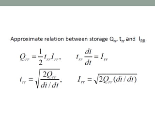
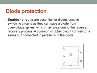
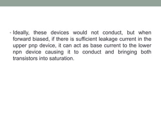
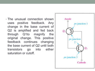
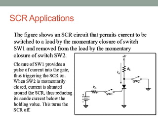
POWER ELECTRONICS
SCT 376-2
DEFINITION
Power electronics involves the study of electronic circuits
intended to control the flow of electrical energy. These
circuits handle power flow at levels much higher than the
individual device ratings.
Rectifiers are probably the most familiar examples of
circuits that meet this definition. Inverters and dc–dc
converters for power supplies are also common
applications.
Power electronics represents a median point at which the
topics of energy systems, electronics, and control converge
and combine. Any useful circuit design for an energy
application must address issues of both devices and
control, as well as of the energy itself.
Among the unique aspects of power electronics are its
emphasis on large semiconductor devices, the application
of magnetic devices for energy storage, special control
methods that must be applied to nonlinear systems, and its
fundamental place as a central component of today’s
energy systems and alternative resources.
• A power electronic system converts electrical energy from
one form to another and ensures the following is
achieved-
• Maximum efficiency
• Maximum reliability
• Maximum availability
• Minimum cost
• Least weight
• Small size
• Applications of Power Electronics are classified into two
types: Static Applications and Drive Applications.
Trends in Power Supplies
Two distinct trends drive electronic power supplies, one of
the major classes of power electronic circuits.
At the high end, microprocessors, memory chips, and other
advanced digital circuits require increasing power levels
and increasing performance at very low voltage. It is a
challenge to deliver 100 A or more efficiently at voltages
that can be less than 1V.
These types of power supplies are expected to deliver
precise voltages, even though the load can change by an
order of magnitude in nanoseconds.
At the other end is the explosive growth of portable devices
with rechargeable batteries. The power supplies for these
devices and for other consumer products must be cheap
and efficient. Losses in low-cost power supplies are a
problem today; often, low-end power supplies and battery
chargers draw energy even when their load is off.
It is increasingly important to use the best possible power
electronics design techniques for these supplies to save
energy while minimizing costs.
Contents of this course :
• High Voltage Power Switching Devices
• Diode Rectifiers
• Adjustable DC/DC converters
• DC/AC and AC/AC Inverters
1. Rashid, M. (2013). Power electronics.,
2. Erickson, R. and Maksimović, D. (2001). Fundamentals of
power electronics. Springer.,
POWER
SEMICONDUCTOR
SWITCHING DEVICES
Classification of power semiconductor
switches
Power devices is divided into terms of their number of
terminals:
–The two-terminal devices (diodes) whose state is
completely dependent on the external power circuit they
are connected to.
–The three-terminal devices, whose state is not only
dependent on their external power circuit, but also on the
signal on their driving terminal (gate or base).
A second classification has to do with the type of
charge carriers they use:
–Some devices are majority carrier devices (Schottky
diode, MOSFET, JFET) - use only one type of charge
carriers (i.e., either electrons or holes)
–Others are minority carrier devices (p-n diode, Thyristor,
BJT, IGBT) - use both charge carriers (i.e. electrons and
holes).
A third classification is based on the degree of
controllability:
• Uncontrollable switches (diodes)
• Semi-controllable switches (thyristors)
• Fully-controllable switches (BJT, MOSFET, JFET, IGBT,
GTO, MCT)
Power Diode
• A power diode has a P-I-N structure as compared to the
signal diode having a P-N structure. Here, I (in P-I-N)
stands for intrinsic semiconductor layer to bear the high-
level reverse voltage as compared to the signal diode.
However, the drawback of this intrinsic layer is that it adds
noticeable resistance during forward-biased condition.
Thus, power diode requires a proper cooling arrangement
for handling large power dissipation. Power diodes are
used in numerous applications including rectifier, voltage
clamper, voltage multiplier and etc.
An ideal diode should have the following
characteristics:
• –When forward-biased, the voltage across the end
terminals of the diode should be zero, whatever the
current that flows through ;
• –When reverse-biased, the leakage current should be
zero, whatever the voltage .
• –The transition between on and off states should be
instantaneous.
Practical Power Diode
• Static Parameters
• – Forward voltage VF
• – Reverse current IR
• – Reverse breakdown voltage VB
• – Forward current IF
• Dynamic Parameters
• – Forward recovery time tfr
• – Reverse recovery time trr
• – Peak reverse recovery current IRR
• – Diode capacitance CD
• – Rate of voltage and current: di/dt, dv/dt
• – Transient thermal resistance (high frequency)
• After the forward diode comes to null, the diode continues
to conduct in the opposite direction because of the
presence of stored charges in the depletion layer and the
p or n-layer.
• The diode current flows for a reverse-recovery time trr. It is
the time between the instant forward diode current
becomes zero and the instant reverse-recovery current
decays to 25 % of its reverse maximum value.
• Time Ta : Charges stored in the depletion layer removed.
• Time Tb : Charges from the semiconductor layer is
removed.
• Shaded area in Fig represents stored charges QR which
must be removed during reverse-recovery time trr.
• Power loss across diode = vf * if
• As shown, major power loss in the diode occurs during
the period tb.
•
• Recovery can be abrupt or smooth. To know it
quantitatively, we can use the S – factor.
•
• Ratio Tb/Ta : Softness factor or S-factor.
• S-factor: measure of the voltage transient that occurs
during the time the diode recovers.
• S-factor = 1 ⇒ low oscillatory reverse-recovery process.
(Soft –recovery diode)
• S-factor <1 ⇒ large oscillatory over voltage (snappy-
recovery diode or fast-recovery diode).
• Power diodes now exist with forward current rating of 1A
to several thousand amperes with reverse-recovery
voltage ratings of 50V to 5000V or more.
Schottky Diode
• It has an aluminum-silicon junction where the silicon is an
n-type. As the metal has no holes, there is no stored
charge and no reverse-recovery time. Therefore, there is
only the movement of the majority carriers (electrons) and
the turn-off delay caused by recombination process is
avoided. It can also switch off much faster than a p-n
junction diode. As compared to the p-n junction diode it
has:
• (a) Lower cut-in voltage
• (b) Higher reverse leakage current
• (c) Higher operating frequency
• Application: high-frequency instrumentation and switching
power supplies.
Schottky Diode Symbol and Current-Voltage Characteristics
Curve
Diode protection
• Snubber circuits are essential for diodes used in
switching circuits as they can save a diode from
overvoltage spikes, which may arise during the reverse
recovery process. A common snubber circuit consists of a
series RC connected in parallel with the diode.
• Series/parallel connections: necessary in high voltage
and high current applications. Matching diode in terms of
their reverse recovery properties is important in order to
avoid large voltage imbalances between the diodes. A
parallel RC snubber in parallel with each diode
overcomes most of these problems.
Assignment 01
• Applications of Diodes:
• Rectifier
• Voltage clamping
• Voltage multiplier …..
• (02 A4 sheets - write on both sides - no cover page –
• Write name and no. on top right corner)
Thyristors
• Thyristors are a class of semiconductor devices
characterized by 4-layers of alternating p and n material.
Four-layer devices act as either open or closed switches;
for this reason, they are most frequently used in control
applications.
• The Thyristor family of semiconductors consists of several
very useful devices. The most widely used of this family
are silicon controlled rectifiers (SCRs), Triacs, SIDACs,
and DIACs.
• In many applications these devices perform key functions
and are real assets in meeting environmental, speed, and
reliability specifications which their electro-mechanical
counterparts cannot fulfill.
• Some thyristors and their symbols
• The 4- layer diode (or Shockley diode) is a type of
thyristor that acts something like an ordinary diode but
conducts in the forward direction only after a certain
anode to cathode voltage called the forward-breakover
voltage is reached.
• The concept of 4- layer devices is usually shown as an
equivalent circuit of a pnp and an npn transistor.
• Ideally, these devices would not conduct, but when
forward biased, if there is sufficient leakage current in the
upper pnp device, it can act as base current to the lower
npn device causing it to conduct and bringing both
transistors into saturation.
• The unusual connection shown
uses positive feedback. Any
change in the base current of
Q2 is amplified and fed back
through Q1to magnify the
original change. This positive
feedback continues changing
the base current of Q2 until both
transistors go into either
saturation or cutoff.
• The only way to turn on the device is by breakover. This
means using a large enough supply voltage to break
down the Q1collector diode. Since the collector current of
Q1increases the base current of Q2, the positive
feedback will start.
• The characteristic curve for a 4- layer diode shows the
forward blocking region. When the anode-to-cathode
voltage exceeds VBR , conduction occurs. The switching
Current at this point is IS
• Once conduction begins, it will continue until anode current
is reduced to less than the holding current(IH). This is the
only way to stop conduction.
Silicon-Controlled Rectifier (SCR)
SCR Specifications
SCR Applications
Example
Half -Wave Power Control
Example
Backup Lighting for Power Interruptions
An Over -Voltage Protection Circuit
Sawtooth Generator
The Diac
The Triac
Triac Applications
Power Electronics
Power Electronics

Power Electronics

  • 1.
  • 2.
    DEFINITION Power electronics involvesthe study of electronic circuits intended to control the flow of electrical energy. These circuits handle power flow at levels much higher than the individual device ratings.
  • 3.
    Rectifiers are probablythe most familiar examples of circuits that meet this definition. Inverters and dc–dc converters for power supplies are also common applications. Power electronics represents a median point at which the topics of energy systems, electronics, and control converge and combine. Any useful circuit design for an energy application must address issues of both devices and control, as well as of the energy itself.
  • 4.
    Among the uniqueaspects of power electronics are its emphasis on large semiconductor devices, the application of magnetic devices for energy storage, special control methods that must be applied to nonlinear systems, and its fundamental place as a central component of today’s energy systems and alternative resources.
  • 5.
    • A powerelectronic system converts electrical energy from one form to another and ensures the following is achieved- • Maximum efficiency • Maximum reliability • Maximum availability • Minimum cost • Least weight • Small size • Applications of Power Electronics are classified into two types: Static Applications and Drive Applications.
  • 6.
    Trends in PowerSupplies Two distinct trends drive electronic power supplies, one of the major classes of power electronic circuits. At the high end, microprocessors, memory chips, and other advanced digital circuits require increasing power levels and increasing performance at very low voltage. It is a challenge to deliver 100 A or more efficiently at voltages that can be less than 1V. These types of power supplies are expected to deliver precise voltages, even though the load can change by an order of magnitude in nanoseconds.
  • 7.
    At the otherend is the explosive growth of portable devices with rechargeable batteries. The power supplies for these devices and for other consumer products must be cheap and efficient. Losses in low-cost power supplies are a problem today; often, low-end power supplies and battery chargers draw energy even when their load is off. It is increasingly important to use the best possible power electronics design techniques for these supplies to save energy while minimizing costs.
  • 8.
    Contents of thiscourse : • High Voltage Power Switching Devices • Diode Rectifiers • Adjustable DC/DC converters • DC/AC and AC/AC Inverters 1. Rashid, M. (2013). Power electronics., 2. Erickson, R. and Maksimović, D. (2001). Fundamentals of power electronics. Springer.,
  • 9.
  • 10.
    Classification of powersemiconductor switches Power devices is divided into terms of their number of terminals: –The two-terminal devices (diodes) whose state is completely dependent on the external power circuit they are connected to. –The three-terminal devices, whose state is not only dependent on their external power circuit, but also on the signal on their driving terminal (gate or base).
  • 11.
    A second classificationhas to do with the type of charge carriers they use: –Some devices are majority carrier devices (Schottky diode, MOSFET, JFET) - use only one type of charge carriers (i.e., either electrons or holes) –Others are minority carrier devices (p-n diode, Thyristor, BJT, IGBT) - use both charge carriers (i.e. electrons and holes).
  • 12.
    A third classificationis based on the degree of controllability: • Uncontrollable switches (diodes) • Semi-controllable switches (thyristors) • Fully-controllable switches (BJT, MOSFET, JFET, IGBT, GTO, MCT)
  • 14.
    Power Diode • Apower diode has a P-I-N structure as compared to the signal diode having a P-N structure. Here, I (in P-I-N) stands for intrinsic semiconductor layer to bear the high- level reverse voltage as compared to the signal diode. However, the drawback of this intrinsic layer is that it adds noticeable resistance during forward-biased condition. Thus, power diode requires a proper cooling arrangement for handling large power dissipation. Power diodes are used in numerous applications including rectifier, voltage clamper, voltage multiplier and etc.
  • 16.
    An ideal diodeshould have the following characteristics: • –When forward-biased, the voltage across the end terminals of the diode should be zero, whatever the current that flows through ; • –When reverse-biased, the leakage current should be zero, whatever the voltage . • –The transition between on and off states should be instantaneous.
  • 18.
    Practical Power Diode •Static Parameters • – Forward voltage VF • – Reverse current IR • – Reverse breakdown voltage VB • – Forward current IF
  • 19.
    • Dynamic Parameters •– Forward recovery time tfr • – Reverse recovery time trr • – Peak reverse recovery current IRR • – Diode capacitance CD • – Rate of voltage and current: di/dt, dv/dt • – Transient thermal resistance (high frequency)
  • 23.
    • After theforward diode comes to null, the diode continues to conduct in the opposite direction because of the presence of stored charges in the depletion layer and the p or n-layer. • The diode current flows for a reverse-recovery time trr. It is the time between the instant forward diode current becomes zero and the instant reverse-recovery current decays to 25 % of its reverse maximum value.
  • 24.
    • Time Ta: Charges stored in the depletion layer removed. • Time Tb : Charges from the semiconductor layer is removed. • Shaded area in Fig represents stored charges QR which must be removed during reverse-recovery time trr. • Power loss across diode = vf * if • As shown, major power loss in the diode occurs during the period tb. •
  • 25.
    • Recovery canbe abrupt or smooth. To know it quantitatively, we can use the S – factor. • • Ratio Tb/Ta : Softness factor or S-factor. • S-factor: measure of the voltage transient that occurs during the time the diode recovers.
  • 26.
    • S-factor =1 ⇒ low oscillatory reverse-recovery process. (Soft –recovery diode) • S-factor <1 ⇒ large oscillatory over voltage (snappy- recovery diode or fast-recovery diode). • Power diodes now exist with forward current rating of 1A to several thousand amperes with reverse-recovery voltage ratings of 50V to 5000V or more.
  • 28.
    Schottky Diode • Ithas an aluminum-silicon junction where the silicon is an n-type. As the metal has no holes, there is no stored charge and no reverse-recovery time. Therefore, there is only the movement of the majority carriers (electrons) and the turn-off delay caused by recombination process is avoided. It can also switch off much faster than a p-n junction diode. As compared to the p-n junction diode it has: • (a) Lower cut-in voltage • (b) Higher reverse leakage current • (c) Higher operating frequency • Application: high-frequency instrumentation and switching power supplies.
  • 29.
    Schottky Diode Symboland Current-Voltage Characteristics Curve
  • 30.
    Diode protection • Snubbercircuits are essential for diodes used in switching circuits as they can save a diode from overvoltage spikes, which may arise during the reverse recovery process. A common snubber circuit consists of a series RC connected in parallel with the diode.
  • 31.
    • Series/parallel connections:necessary in high voltage and high current applications. Matching diode in terms of their reverse recovery properties is important in order to avoid large voltage imbalances between the diodes. A parallel RC snubber in parallel with each diode overcomes most of these problems.
  • 32.
    Assignment 01 • Applicationsof Diodes: • Rectifier • Voltage clamping • Voltage multiplier ….. • (02 A4 sheets - write on both sides - no cover page – • Write name and no. on top right corner)
  • 33.
    Thyristors • Thyristors area class of semiconductor devices characterized by 4-layers of alternating p and n material. Four-layer devices act as either open or closed switches; for this reason, they are most frequently used in control applications.
  • 34.
    • The Thyristorfamily of semiconductors consists of several very useful devices. The most widely used of this family are silicon controlled rectifiers (SCRs), Triacs, SIDACs, and DIACs. • In many applications these devices perform key functions and are real assets in meeting environmental, speed, and reliability specifications which their electro-mechanical counterparts cannot fulfill.
  • 35.
    • Some thyristorsand their symbols
  • 36.
    • The 4-layer diode (or Shockley diode) is a type of thyristor that acts something like an ordinary diode but conducts in the forward direction only after a certain anode to cathode voltage called the forward-breakover voltage is reached.
  • 37.
    • The conceptof 4- layer devices is usually shown as an equivalent circuit of a pnp and an npn transistor.
  • 38.
    • Ideally, thesedevices would not conduct, but when forward biased, if there is sufficient leakage current in the upper pnp device, it can act as base current to the lower npn device causing it to conduct and bringing both transistors into saturation.
  • 39.
    • The unusualconnection shown uses positive feedback. Any change in the base current of Q2 is amplified and fed back through Q1to magnify the original change. This positive feedback continues changing the base current of Q2 until both transistors go into either saturation or cutoff.
  • 40.
    • The onlyway to turn on the device is by breakover. This means using a large enough supply voltage to break down the Q1collector diode. Since the collector current of Q1increases the base current of Q2, the positive feedback will start.
  • 41.
    • The characteristiccurve for a 4- layer diode shows the forward blocking region. When the anode-to-cathode voltage exceeds VBR , conduction occurs. The switching Current at this point is IS • Once conduction begins, it will continue until anode current is reduced to less than the holding current(IH). This is the only way to stop conduction.
  • 42.
  • 45.
  • 46.
  • 47.
  • 48.
  • 50.
  • 51.
    Backup Lighting forPower Interruptions
  • 52.
    An Over -VoltageProtection Circuit
  • 53.
  • 55.
  • 57.
  • 60.