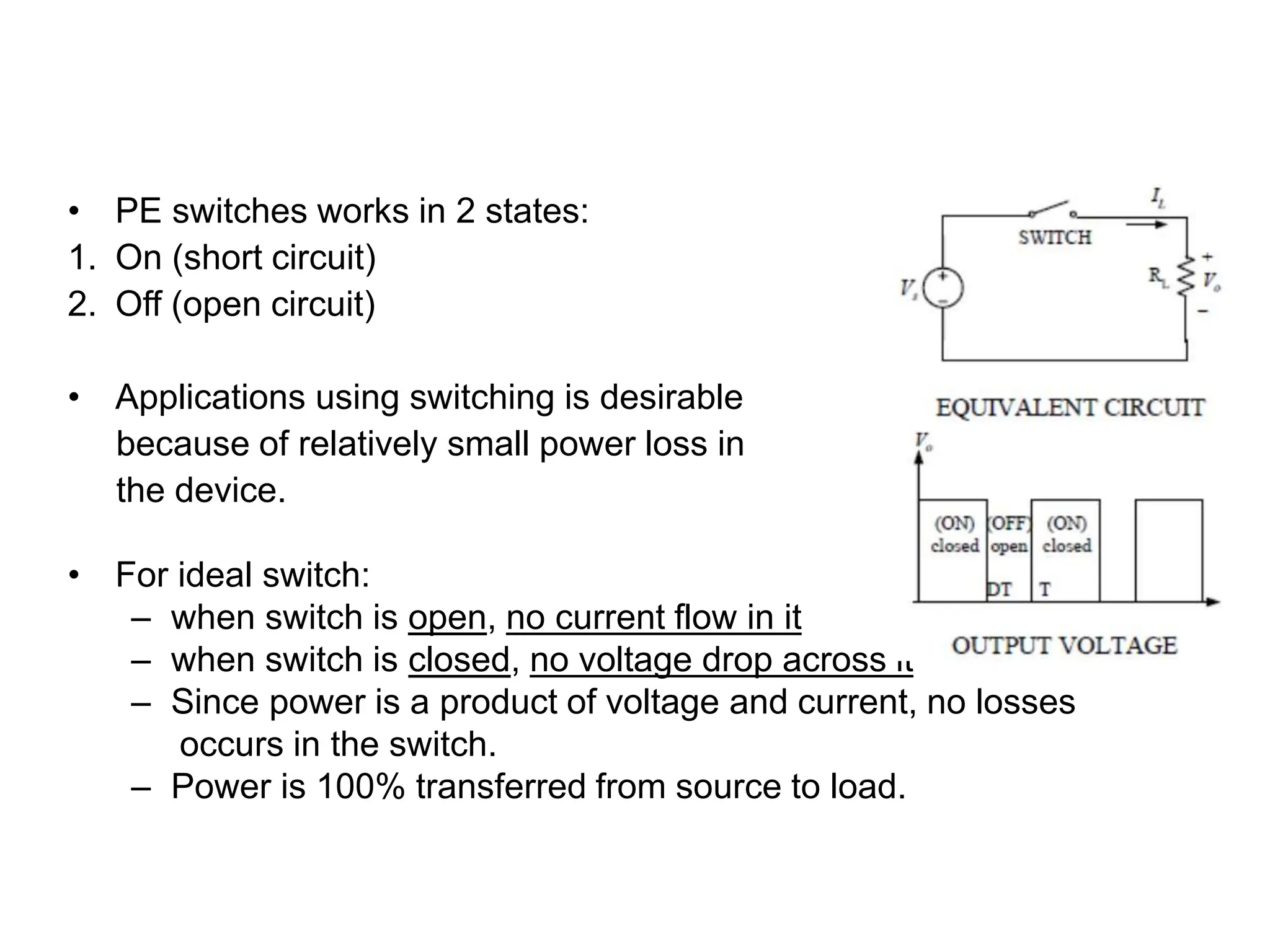
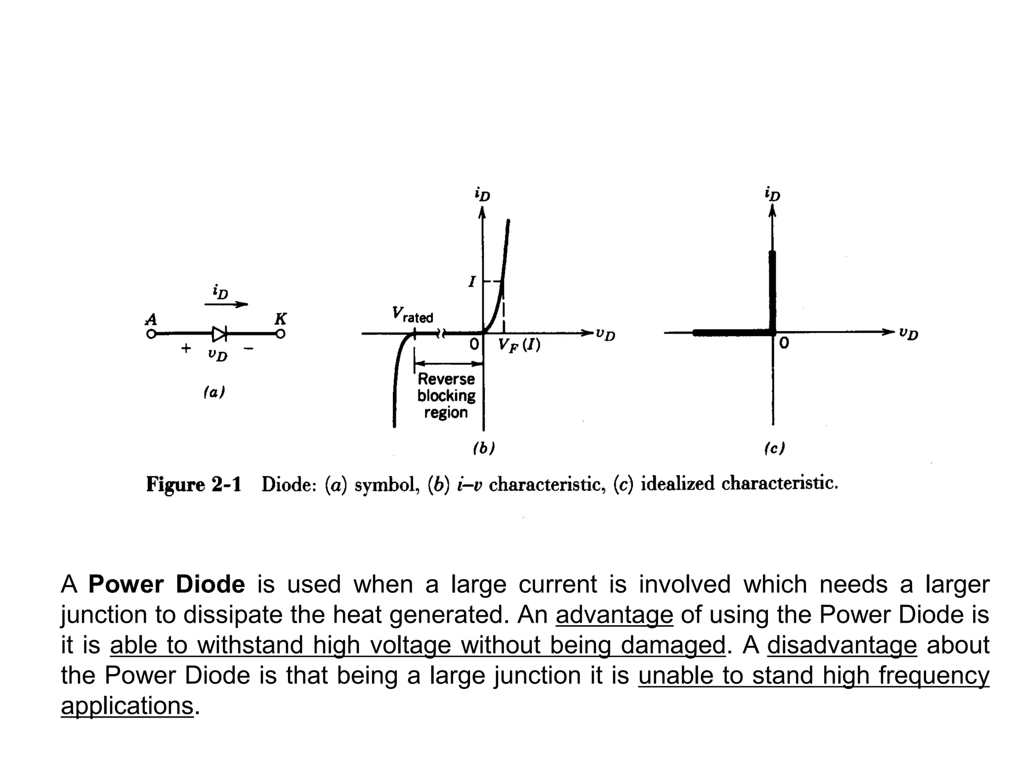
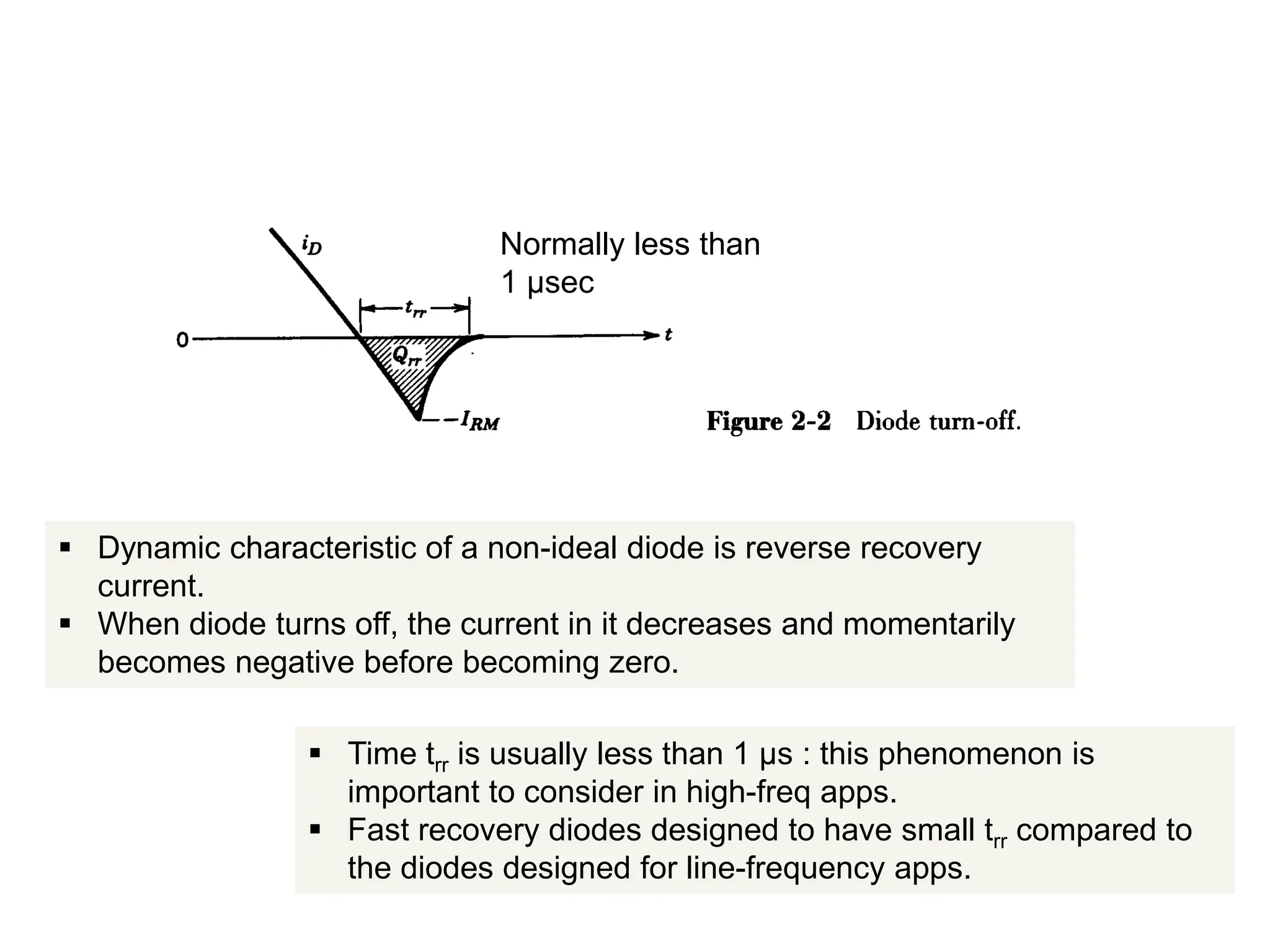
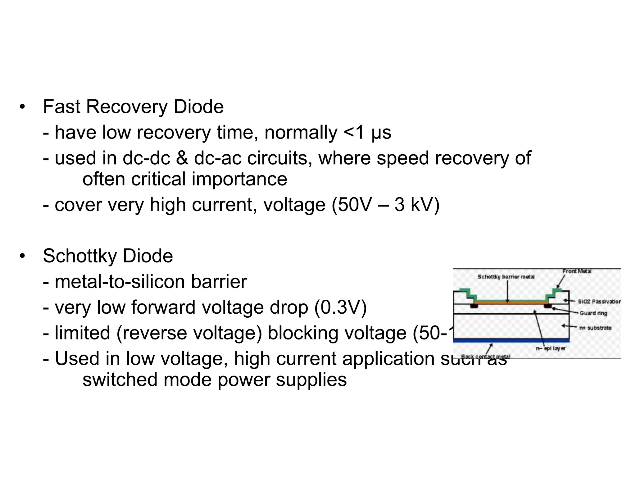
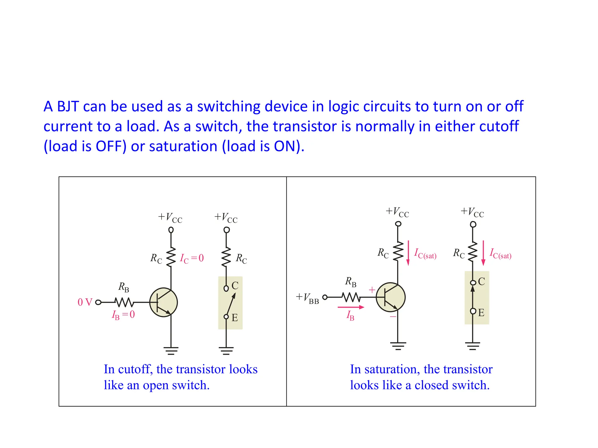
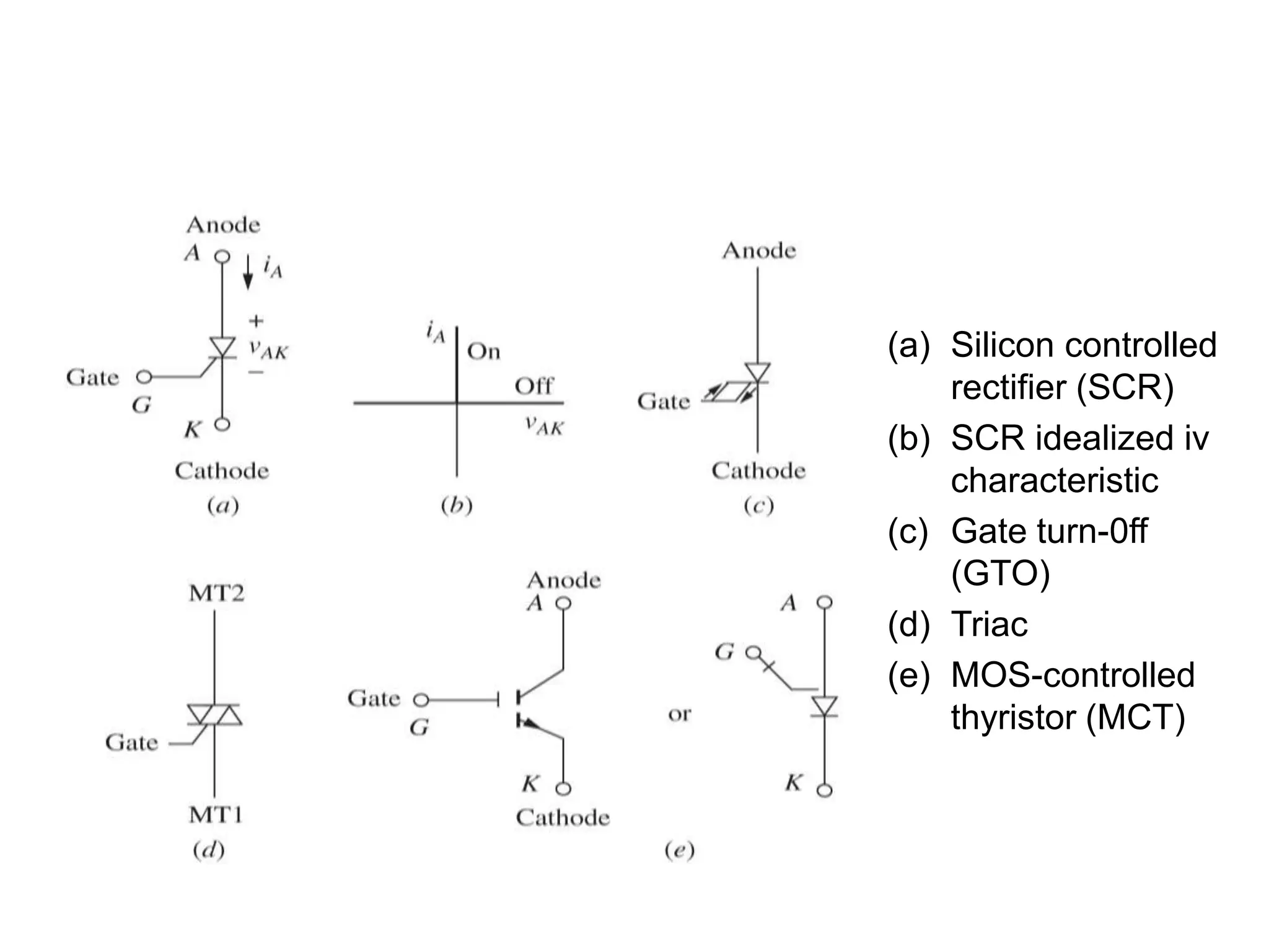
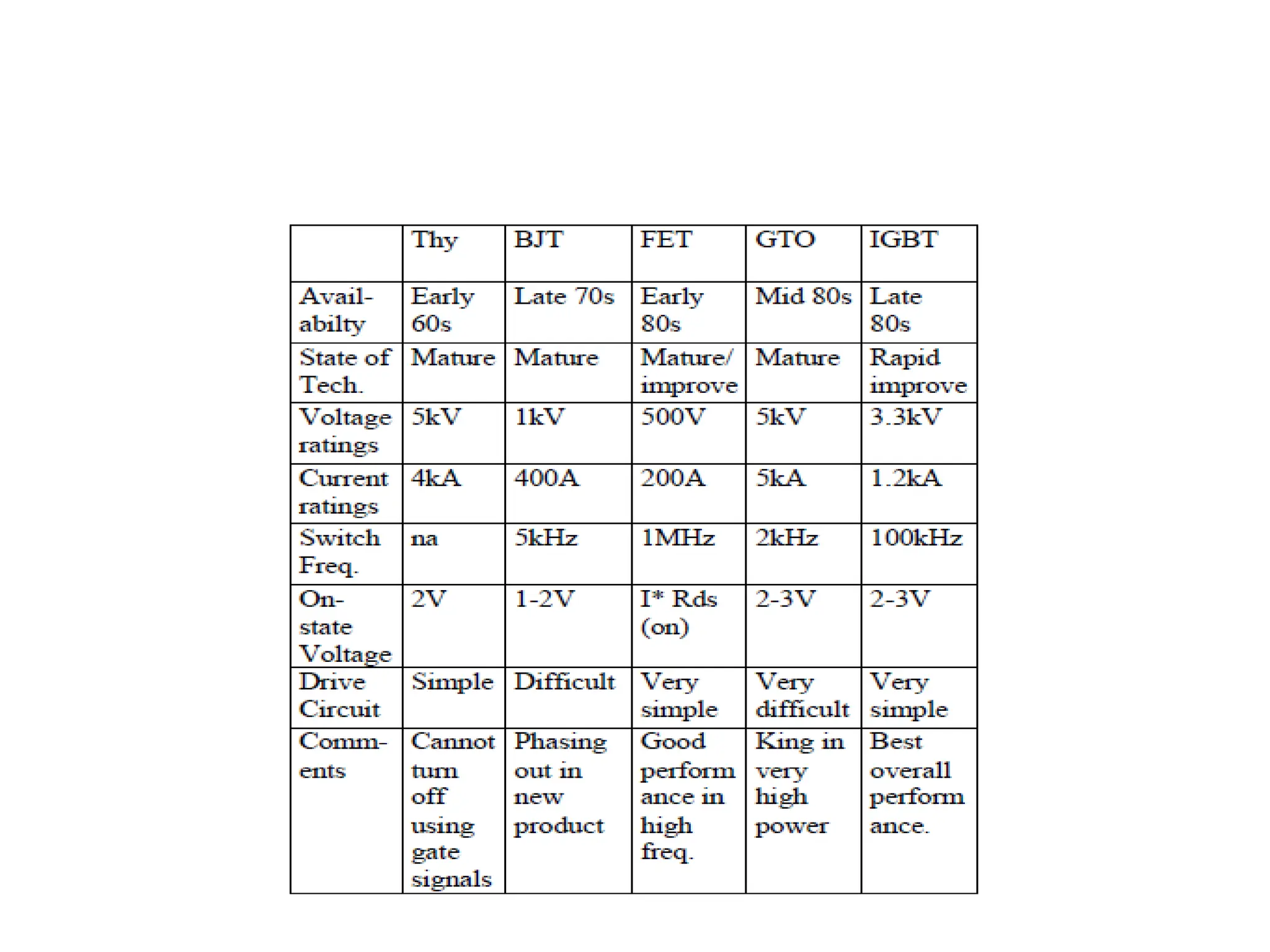
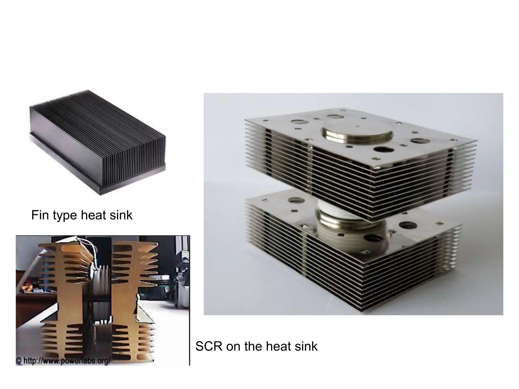
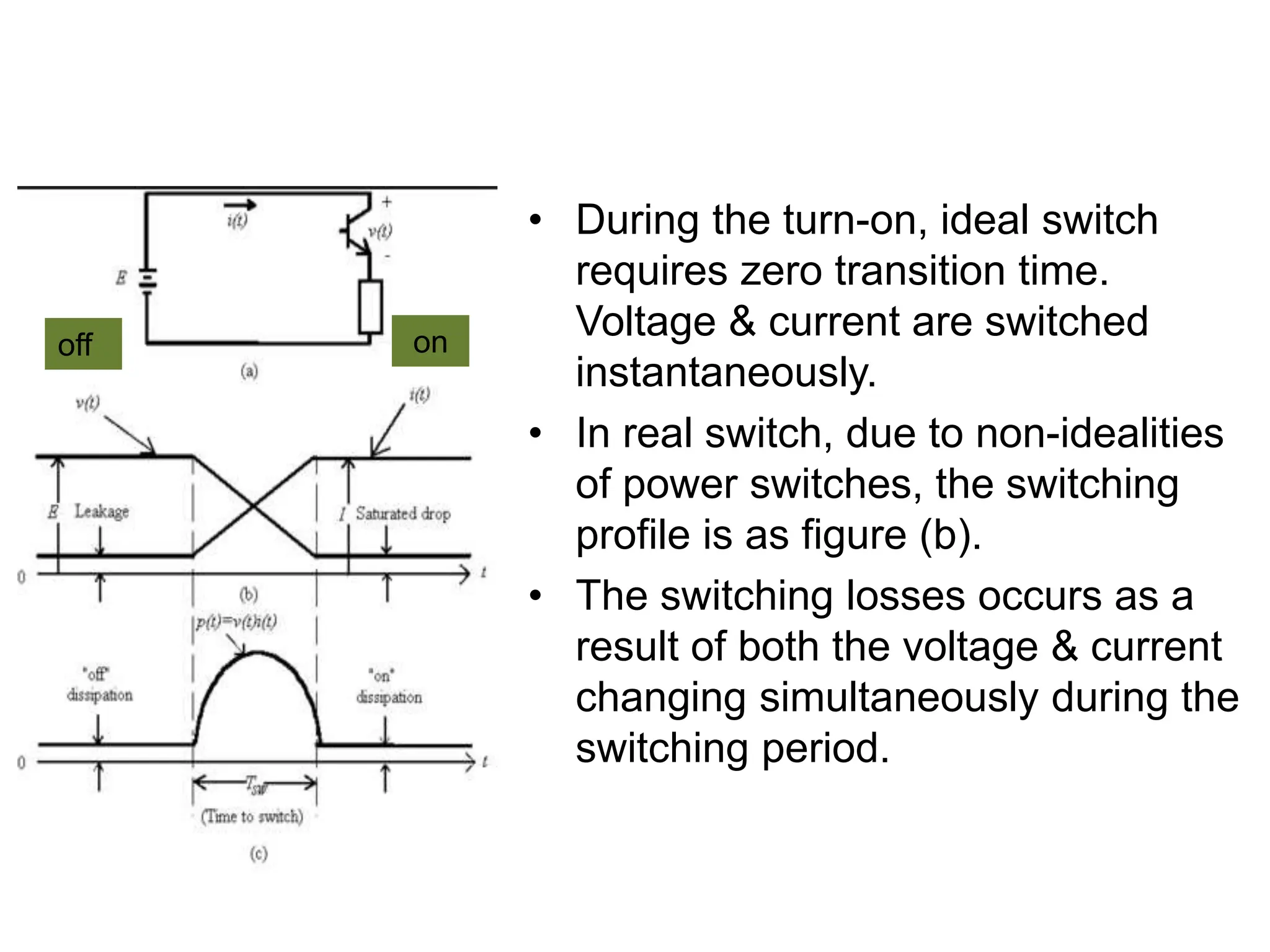
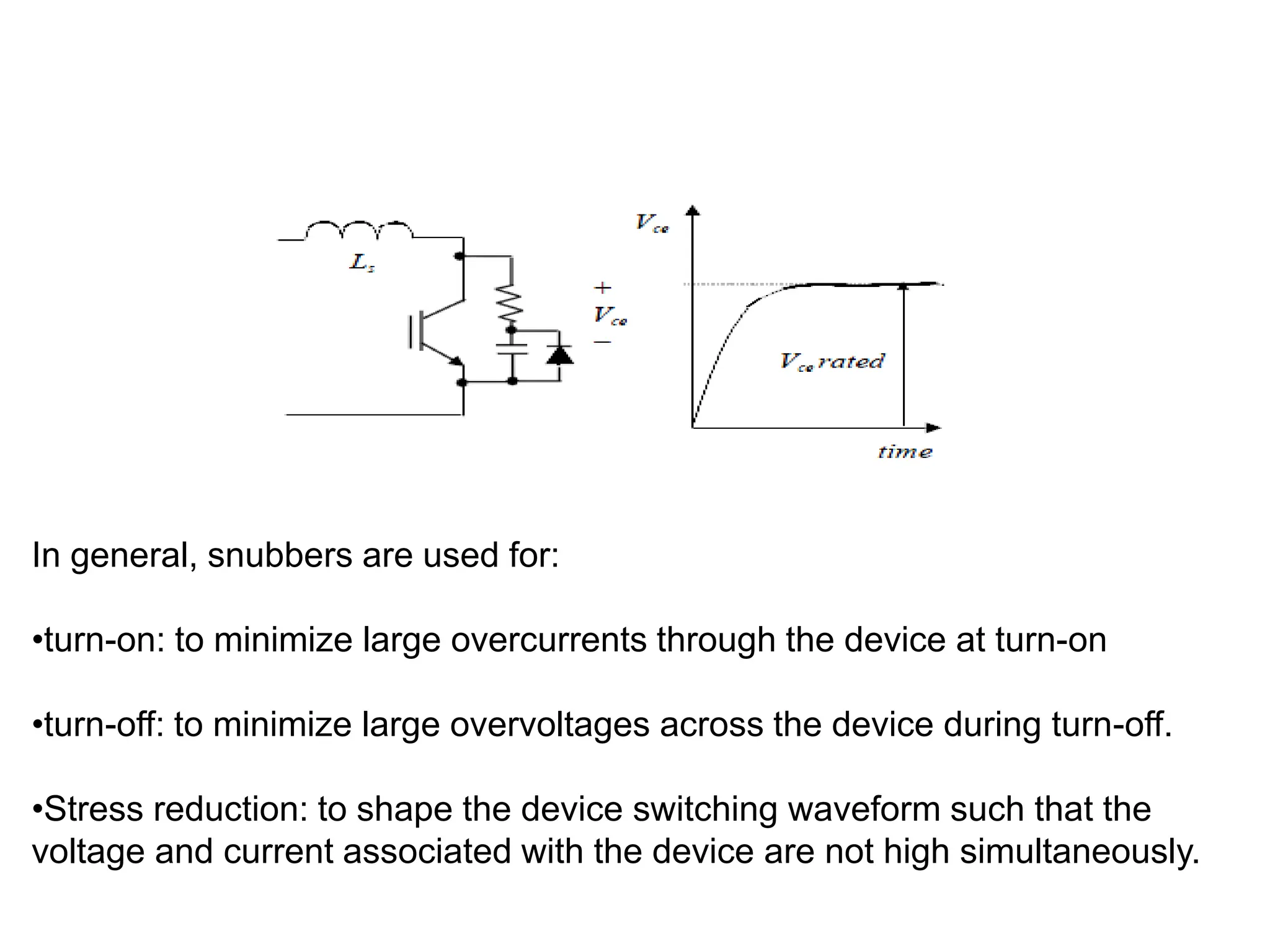
POWER SEMICONDUCTOR
DEVICES
POWER SWITCHES
• PE switches works in 2 states:
1. On (short circuit)
2. Off (open circuit)
• Applications using switching is desirable
because of relatively small power loss in
the device.
• For ideal switch:
– when switch is open, no current flow in it
– when switch is closed, no voltage drop across it
– Since power is a product of voltage and current, no losses
occurs in the switch.
– Power is 100% transferred from source to load.
DIODE
• Uncontrollable switch : on/off conditions is determined by
voltages & currents in the circuit.
• On : The diode is forward biased (when the current, iD
positive)
• Off : The diode is reversed-biased (when vD is negative)
• Reverse recovery time, trr is the time required for the
diode to be off & its current become zero.
DIODE CHARACTERISTIC
A Power Diode is used when a large current is involved which needs a larger
junction to dissipate the heat generated. An advantage of using the Power Diode is
it is able to withstand high voltage without being damaged. A disadvantage about
the Power Diode is that being a large junction it is unable to stand high frequency
applications.
REVERSE RECOVERY TIME IN
POWER DIODE
 Dynamic characteristic of a non-ideal diode is reverse recovery
current.
 When diode turns off, the current in it decreases and momentarily
becomes negative before becoming zero.
 Time trr is usually less than 1 µs : this phenomenon is
important to consider in high-freq apps.
 Fast recovery diodes designed to have small trr compared to
the diodes designed for line-frequency apps.
Normally less than
1 µsec
TYPES OF DIODES
• Line Frequency (General Purpose Diode)
- relatively have high reverse recovery time, trr = 25 µs
- used in low speed applications (where trr is not critical)
- eg : diode rectifiers & converters for a low input
frequency up to 1kHz apps.
- cover very high current (up to 5 kA) & voltage (5 kV)
rating
• Fast Recovery Diode
- have low recovery time, normally <1 µs
- used in dc-dc & dc-ac circuits, where speed recovery of
often critical importance
- cover very high current, voltage (50V – 3 kV)
• Schottky Diode
- metal-to-silicon barrier
- very low forward voltage drop (0.3V)
- limited (reverse voltage) blocking voltage (50-100V)
- Used in low voltage, high current application such as
switched mode power supplies
TYPES OF DIODES
TRANSISTORS – BIPOLAR
JUNCTION TRANSISTOR (BJT)
• On-state is achieved by providing sufficient base current to
derive the BJT into saturation.
• Rating : Voltage (VCE <1000V), current (IC <400A), switching
frequency (up to 5 kHz), Low on-state voltage (VCE(SAT) = 2-
3V)
• Off state is achieved when base current is zero
• Power BJT is a current controlled device and it has low gain
hfe value (<20). Need high base current to obtain reasonable
IC.
• Darlington configurations have 2 connected BJTs. The
effective current gain of combination is approximately the
product of 2 individual gains and thus reduce the current
required from the drive circuit.
TRANSISTORS – BIPOLAR
JUNCTION TRANSISTOR (BJT)
(d) Darlington connection
BJT as a Switch - RecaP
A BJT can be used as a switching device in logic circuits to turn on or off
current to a load. As a switch, the transistor is normally in either cutoff
(load is OFF) or saturation (load is ON).
In cutoff, the transistor looks
like an open switch.
In saturation, the transistor
looks like a closed switch.
RB
0 V
RC IC =0
+VCC
RC
C
E
+VCC
IB =0 –
+
RB
RC IC(sat)
+VCC
RC
C
E
+VCC
IB
+VBB
IC(sat)
TRANSISTORS – MOSFET
• MOSFET is a voltage-controlled device & can be used in PE
circuits. Power MOSFET are the enhancement type rather than the
depletion type.
• A sufficient large gate-to-source voltage will turn the device on, and
when the VGS is 0V it will turn off.
• In on-state, the change of VDC is linearly proportional to the change
in iD. Thus, the MOSFET can be modelled as an on-state resistance
RDC(on) (few miliohms).
• MOSFET is optimal for low-voltage operation at high switching
frequencies.
• Ratings can be up to 1500V & more than 600A. Switching
frequency up to MHz.
• MOSFET is dominant in high frequency applications (>100kHz).
Biggest application is in SMPS.
TRANSISTORS – MOSFET
TRANSISTORS – INSULATED-GATE
BIPOLAR TRANSISTOR (IGBT)
• IGBT is an integrated connection of a MOSFET & BJT.
• IGBT circuit is similar as for MOSFET, while the on state
characteristics are like those of the BJT.
• Low losses like BJT due to low on state collector emitter
voltage (2-3V)
• For very high power devices & applications, frequency is
limited to several kHz.
• IGBT has replaced BJTs in many applications.
(a) Equivalent circuits
(b) Circuit symbols
TRANSISTORS – INSULATED-GATE
BIPOLAR TRANSISTOR (IGBT)
THYRISTOR
• Thyristor are electronic switches used in some PE circuits where
the control switch on is required.
• Thyristor is a 3 terminal devices include the silicon controlled
rectifier (SCR), triac, gate turn-off thyristor (GTO), & MOS-
controlled thyristor (MCT).
• Thyristor are capable of large currents and large blocking
voltages for use in high-power application, but switching
frequencies cannot be as high as when using other devices such
as MOSFETs.
• For SCR to begin to conduct, it must have gate current
applied while positive anode-to-cathode voltage.
• After connection established, the gate signal no longer
required to maintain the anode current.
• The SCR will continue to conduct as long as the anode
current remains positive & above the minimum value
called the holding level.
THYRISTOR
THYRISTOR
(a) Silicon controlled
rectifier (SCR)
(b) SCR idealized iv
characteristic
(c) Gate turn-0ff
(GTO)
(d) Triac
(e) MOS-controlled
thyristor (MCT)
THYRISTOR
• GTO is turned on by a short-duration gate current if the
anode-to-cathode voltage is positive & can be turned off with
a negative gate current which make the design of gate drive
quite difficult. It has slow switching speed & it is used at very
high power levels.
• Triac thyristor is capable of conducting current either in either
direction. It is equivalent to 2 antiparallel SCRs.
• For MCT, the function is equivalent to GTO but without high
turn off gate current requirement. It has SCR & 2 MOSFET
integrated in a device. It can be turn on and off by establishing
the proper voltage from gate to cathode as opposed to
establishing gate current to the GTO.
THYRISTOR
• Selection of power device for an application is depends on
the required voltage, current levels & its switching
characteristics.
• Transistors & GTOs provide control of both turn-on & turn-off ,
SCR provide turn on but not turn off & diodes are neither.
• MOSFET has the advantage in switching speed over BJT
since it is a majority carrier storage delay.
• MOSFET has lower switching losses compared to BJT since
it has shorter switching time
• The switching device selection depends on the required
operating point & turn on & turn off characteristics.
SWITCH SELECTION
SWITCHES COMPARISON
2000
SWITCHES
Power diode
Thyristors
Power mosfet
Power BJT
IGBT
• It is important to consider losses of power switches:
- To ensure that the system operates reliably under prescribed
ambient consition.
- Heat removal mechanism (eg. Heat sink, radiators, coolant) can be
specified.
- Losses in switches affects efficiency.
• Heat sink & other heat removal are costly & bulky. It can be
substantial cost of the total system.
• If a power switch is not cooled to its specified junction temperature,
the full power capability of the switch cannot be realized. (derating
of power switch ratings may be necessary)
POWER SWITCH LOSSES
POWER SWITCH LOSSES
Main losses occurs in
power switch
Forward conduction
losses
Blocking state
losses
Switching
losses
Fin type heat sink
SCR on the heat sink
HEAT SINKS
• No current can flow when the switch is off, and when it is
on, current can flow in the direction of the arrow only.
• Ideal switch has zero voltage drop across it during turn on,
Von. Although the forward current is large, the losses at the
switch is zero.
• But for real switches such as BJT, IGBT, GTO, SCR have
forward conduction voltage which is characterized by the
RDS (on)
FORWARD CONDUCTION LOSSES
• Losses is measured by product of voltage drop across the
device, Von with the current, Ion, averaged over a period.
• Forward conduction losses is the major source of loss at low
frequency & DC operation.
• During turn-off, the switch blocks large voltage. Ideally no
current should flow through the switch. But for real switch, a
small amount of leakage current may flow. This creates turn-
off/blocking state losses.
• The leakage current during turn-off is normally small, hence,
the turn-off losses are usually neglected.
FORWARD CONDUCTION &
BLOCKING STATE LOSSES
• The product of device voltage & current gives instantaneous
power dissipated in the device.
• The heat energy that developed over the switching period is
the integration (summation) of instantaneous power over
time as shown by the shaded area under the power curve.
• The average power loss is the sum of the turn-on & turn-off
energies multiplied with the switching frequency.
• When the frequency increase, switching losses increase.
This limits the usable range of power switches unless proper
heat removal mechanism is employed.
FORWARD CONDUCTION &
BLOCKING STATE LOSSES
SWITCHING LOSSES
• During the turn-on, ideal switch
requires zero transition time.
Voltage & current are switched
instantaneously.
• In real switch, due to non-idealities
of power switches, the switching
profile is as figure (b).
• The switching losses occurs as a
result of both the voltage & current
changing simultaneously during the
switching period.
off on
SNUBBER CIRCUIT
SNUBBER CIRCUIT
• From previous equation, the voltage across the switch is bigger
than the supply (for a short moment).
• The spike may exceed the switch rated blocking voltage and
causes damage due to overvoltage.
• To prevent such occurrence, a snubber is put across the switch.
An example of a snubber is an RCD circuit.
• Snubber circuit “smoothened” the transition and make the switch
voltage rise more “slowly”. In effect it dampens the high voltage
spike to a safe value.
• BJT switches and diodes requires snubbers. However, new
generation of IGBT,MOSFET and GCT do not require it.
RCD SNUBBER CIRCUIT
In general, snubbers are used for:
•turn-on: to minimize large overcurrents through the device at turn-on
•turn-off: to minimize large overvoltages across the device during turn-off.
•Stress reduction: to shape the device switching waveform such that the
voltage and current associated with the device are not high simultaneously.

308557074-POWER-SEMICONDUCTOR-DEVICES-ppt.ppt

  • 1.
  • 2.
    POWER SWITCHES • PEswitches works in 2 states: 1. On (short circuit) 2. Off (open circuit) • Applications using switching is desirable because of relatively small power loss in the device. • For ideal switch: – when switch is open, no current flow in it – when switch is closed, no voltage drop across it – Since power is a product of voltage and current, no losses occurs in the switch. – Power is 100% transferred from source to load.
  • 3.
    DIODE • Uncontrollable switch: on/off conditions is determined by voltages & currents in the circuit. • On : The diode is forward biased (when the current, iD positive) • Off : The diode is reversed-biased (when vD is negative) • Reverse recovery time, trr is the time required for the diode to be off & its current become zero.
  • 4.
    DIODE CHARACTERISTIC A PowerDiode is used when a large current is involved which needs a larger junction to dissipate the heat generated. An advantage of using the Power Diode is it is able to withstand high voltage without being damaged. A disadvantage about the Power Diode is that being a large junction it is unable to stand high frequency applications.
  • 5.
    REVERSE RECOVERY TIMEIN POWER DIODE  Dynamic characteristic of a non-ideal diode is reverse recovery current.  When diode turns off, the current in it decreases and momentarily becomes negative before becoming zero.  Time trr is usually less than 1 µs : this phenomenon is important to consider in high-freq apps.  Fast recovery diodes designed to have small trr compared to the diodes designed for line-frequency apps. Normally less than 1 µsec
  • 6.
    TYPES OF DIODES •Line Frequency (General Purpose Diode) - relatively have high reverse recovery time, trr = 25 µs - used in low speed applications (where trr is not critical) - eg : diode rectifiers & converters for a low input frequency up to 1kHz apps. - cover very high current (up to 5 kA) & voltage (5 kV) rating
  • 7.
    • Fast RecoveryDiode - have low recovery time, normally <1 µs - used in dc-dc & dc-ac circuits, where speed recovery of often critical importance - cover very high current, voltage (50V – 3 kV) • Schottky Diode - metal-to-silicon barrier - very low forward voltage drop (0.3V) - limited (reverse voltage) blocking voltage (50-100V) - Used in low voltage, high current application such as switched mode power supplies TYPES OF DIODES
  • 8.
    TRANSISTORS – BIPOLAR JUNCTIONTRANSISTOR (BJT) • On-state is achieved by providing sufficient base current to derive the BJT into saturation. • Rating : Voltage (VCE <1000V), current (IC <400A), switching frequency (up to 5 kHz), Low on-state voltage (VCE(SAT) = 2- 3V) • Off state is achieved when base current is zero • Power BJT is a current controlled device and it has low gain hfe value (<20). Need high base current to obtain reasonable IC. • Darlington configurations have 2 connected BJTs. The effective current gain of combination is approximately the product of 2 individual gains and thus reduce the current required from the drive circuit.
  • 9.
    TRANSISTORS – BIPOLAR JUNCTIONTRANSISTOR (BJT) (d) Darlington connection
  • 10.
    BJT as aSwitch - RecaP A BJT can be used as a switching device in logic circuits to turn on or off current to a load. As a switch, the transistor is normally in either cutoff (load is OFF) or saturation (load is ON). In cutoff, the transistor looks like an open switch. In saturation, the transistor looks like a closed switch. RB 0 V RC IC =0 +VCC RC C E +VCC IB =0 – + RB RC IC(sat) +VCC RC C E +VCC IB +VBB IC(sat)
  • 11.
    TRANSISTORS – MOSFET •MOSFET is a voltage-controlled device & can be used in PE circuits. Power MOSFET are the enhancement type rather than the depletion type. • A sufficient large gate-to-source voltage will turn the device on, and when the VGS is 0V it will turn off. • In on-state, the change of VDC is linearly proportional to the change in iD. Thus, the MOSFET can be modelled as an on-state resistance RDC(on) (few miliohms). • MOSFET is optimal for low-voltage operation at high switching frequencies. • Ratings can be up to 1500V & more than 600A. Switching frequency up to MHz. • MOSFET is dominant in high frequency applications (>100kHz). Biggest application is in SMPS.
  • 12.
  • 13.
    TRANSISTORS – INSULATED-GATE BIPOLARTRANSISTOR (IGBT) • IGBT is an integrated connection of a MOSFET & BJT. • IGBT circuit is similar as for MOSFET, while the on state characteristics are like those of the BJT. • Low losses like BJT due to low on state collector emitter voltage (2-3V) • For very high power devices & applications, frequency is limited to several kHz. • IGBT has replaced BJTs in many applications.
  • 14.
    (a) Equivalent circuits (b)Circuit symbols TRANSISTORS – INSULATED-GATE BIPOLAR TRANSISTOR (IGBT)
  • 15.
    THYRISTOR • Thyristor areelectronic switches used in some PE circuits where the control switch on is required. • Thyristor is a 3 terminal devices include the silicon controlled rectifier (SCR), triac, gate turn-off thyristor (GTO), & MOS- controlled thyristor (MCT). • Thyristor are capable of large currents and large blocking voltages for use in high-power application, but switching frequencies cannot be as high as when using other devices such as MOSFETs.
  • 16.
    • For SCRto begin to conduct, it must have gate current applied while positive anode-to-cathode voltage. • After connection established, the gate signal no longer required to maintain the anode current. • The SCR will continue to conduct as long as the anode current remains positive & above the minimum value called the holding level. THYRISTOR THYRISTOR
  • 17.
    (a) Silicon controlled rectifier(SCR) (b) SCR idealized iv characteristic (c) Gate turn-0ff (GTO) (d) Triac (e) MOS-controlled thyristor (MCT) THYRISTOR
  • 18.
    • GTO isturned on by a short-duration gate current if the anode-to-cathode voltage is positive & can be turned off with a negative gate current which make the design of gate drive quite difficult. It has slow switching speed & it is used at very high power levels. • Triac thyristor is capable of conducting current either in either direction. It is equivalent to 2 antiparallel SCRs. • For MCT, the function is equivalent to GTO but without high turn off gate current requirement. It has SCR & 2 MOSFET integrated in a device. It can be turn on and off by establishing the proper voltage from gate to cathode as opposed to establishing gate current to the GTO. THYRISTOR
  • 19.
    • Selection ofpower device for an application is depends on the required voltage, current levels & its switching characteristics. • Transistors & GTOs provide control of both turn-on & turn-off , SCR provide turn on but not turn off & diodes are neither. • MOSFET has the advantage in switching speed over BJT since it is a majority carrier storage delay. • MOSFET has lower switching losses compared to BJT since it has shorter switching time • The switching device selection depends on the required operating point & turn on & turn off characteristics. SWITCH SELECTION
  • 20.
  • 21.
  • 22.
    • It isimportant to consider losses of power switches: - To ensure that the system operates reliably under prescribed ambient consition. - Heat removal mechanism (eg. Heat sink, radiators, coolant) can be specified. - Losses in switches affects efficiency. • Heat sink & other heat removal are costly & bulky. It can be substantial cost of the total system. • If a power switch is not cooled to its specified junction temperature, the full power capability of the switch cannot be realized. (derating of power switch ratings may be necessary) POWER SWITCH LOSSES
  • 23.
    POWER SWITCH LOSSES Mainlosses occurs in power switch Forward conduction losses Blocking state losses Switching losses
  • 24.
    Fin type heatsink SCR on the heat sink HEAT SINKS
  • 25.
    • No currentcan flow when the switch is off, and when it is on, current can flow in the direction of the arrow only. • Ideal switch has zero voltage drop across it during turn on, Von. Although the forward current is large, the losses at the switch is zero. • But for real switches such as BJT, IGBT, GTO, SCR have forward conduction voltage which is characterized by the RDS (on) FORWARD CONDUCTION LOSSES
  • 26.
    • Losses ismeasured by product of voltage drop across the device, Von with the current, Ion, averaged over a period. • Forward conduction losses is the major source of loss at low frequency & DC operation. • During turn-off, the switch blocks large voltage. Ideally no current should flow through the switch. But for real switch, a small amount of leakage current may flow. This creates turn- off/blocking state losses. • The leakage current during turn-off is normally small, hence, the turn-off losses are usually neglected. FORWARD CONDUCTION & BLOCKING STATE LOSSES
  • 27.
    • The productof device voltage & current gives instantaneous power dissipated in the device. • The heat energy that developed over the switching period is the integration (summation) of instantaneous power over time as shown by the shaded area under the power curve. • The average power loss is the sum of the turn-on & turn-off energies multiplied with the switching frequency. • When the frequency increase, switching losses increase. This limits the usable range of power switches unless proper heat removal mechanism is employed. FORWARD CONDUCTION & BLOCKING STATE LOSSES
  • 28.
    SWITCHING LOSSES • Duringthe turn-on, ideal switch requires zero transition time. Voltage & current are switched instantaneously. • In real switch, due to non-idealities of power switches, the switching profile is as figure (b). • The switching losses occurs as a result of both the voltage & current changing simultaneously during the switching period. off on
  • 29.
  • 30.
    SNUBBER CIRCUIT • Fromprevious equation, the voltage across the switch is bigger than the supply (for a short moment). • The spike may exceed the switch rated blocking voltage and causes damage due to overvoltage. • To prevent such occurrence, a snubber is put across the switch. An example of a snubber is an RCD circuit. • Snubber circuit “smoothened” the transition and make the switch voltage rise more “slowly”. In effect it dampens the high voltage spike to a safe value. • BJT switches and diodes requires snubbers. However, new generation of IGBT,MOSFET and GCT do not require it.
  • 31.
    RCD SNUBBER CIRCUIT Ingeneral, snubbers are used for: •turn-on: to minimize large overcurrents through the device at turn-on •turn-off: to minimize large overvoltages across the device during turn-off. •Stress reduction: to shape the device switching waveform such that the voltage and current associated with the device are not high simultaneously.

Editor's Notes

  • #4 - The simplest electronic switch
  • #9 The Rating of an electrical appliance indicates the voltage at which the appliance is designed to work and the current consumption at that voltage
  • #10 Darlington configurations have 2 connected BJTs. The effective current gain of combination is approximately the product of 2 individual gains and thus reduce the current required from the drive circuit.
  • #15 • Ratings: Voltage: VCE<3.3kV, Current,:IC<1.2kA currently available. Work in under progress for 4.5kV/1.2kA device.Constant improvement in voltage and current ratings • Good switching capability (up to 100KHz) for newer devices. Typical application, IGBT is used at 20-50KHz.
  • #26 Mosfet on resistance .. Rds (on)
  • #28 The snubber provides a short-term alternative current path around the current switching device so that the inductive element may be discharged more safely and quietly. Inductive elements are often unintentional, but arise from the current loops implied by physical circuitry. While current switching is everywhere, snubbers will generally only be required where a major current path is switched, such as in power supplies.
  • #32 The snubber provides a short-term alternative current path around the current switching device so that the inductive element may be discharged more safely and quietly. Inductive elements are often unintentional, but arise from the current loops implied by physical circuitry. While current switching is everywhere, snubbers will generally only be required where a major current path is switched, such as in power supplies.