Downloaded 196 times
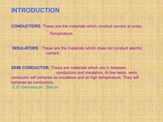
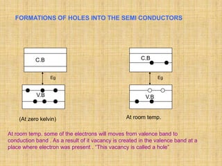
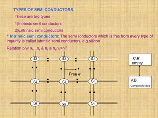

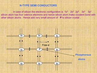
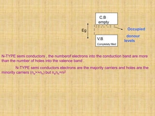
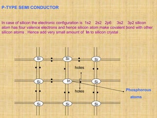
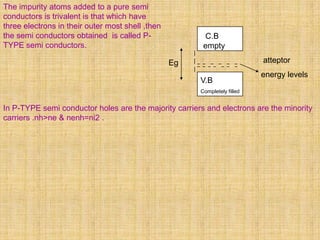


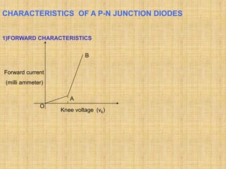
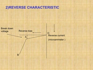
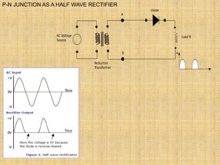


This document discusses semiconductors and semiconductor devices. It begins by distinguishing between conductors, insulators, and semiconductors. Semiconductors can behave as either insulators or conductors depending on temperature. It then discusses the formation of holes in semiconductors and types of semiconductors including intrinsic and extrinsic (n-type and p-type) semiconductors. The document outlines the basic operation and characteristics of common semiconductor devices like diodes and their usage in rectification. It concludes by listing some advantages of semiconductor devices like their small size and weight compared to vacuum tubes.