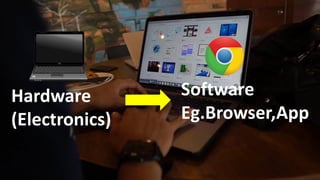
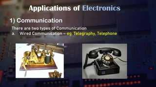
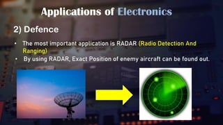
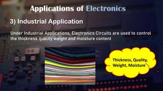
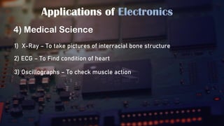
1) The document discusses basic electronics concepts including why we learn electronics, what electronics is, and applications of electronics such as communication, defense, industrial uses, and medical science.
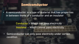
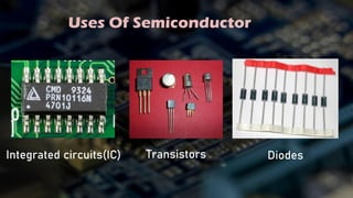
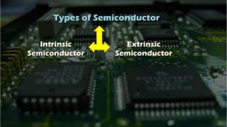
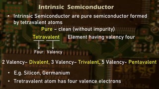
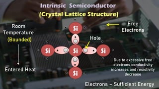
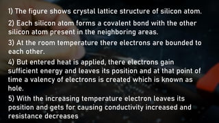
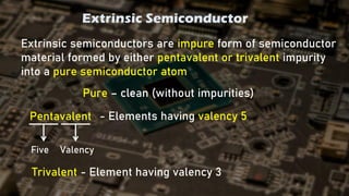
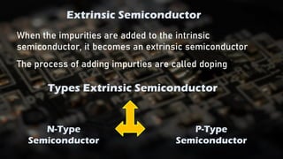
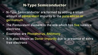
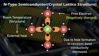
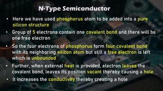
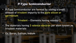
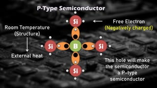
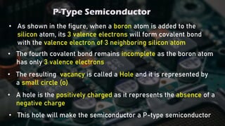
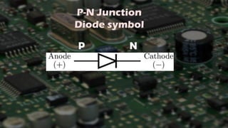
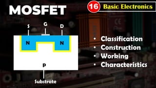
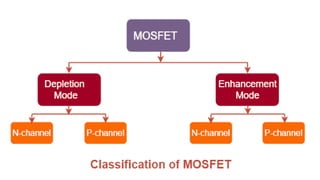
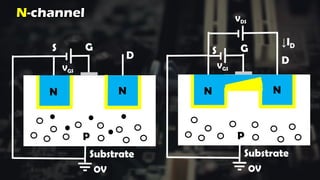
2) It also covers semiconductor concepts like intrinsic and extrinsic semiconductors, and how doping with n-type and p-type materials creates a p-n junction in a diode.
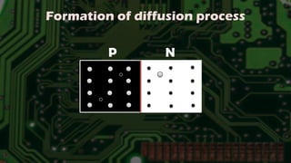
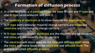
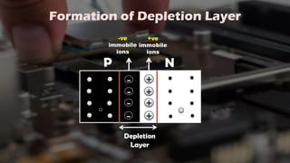
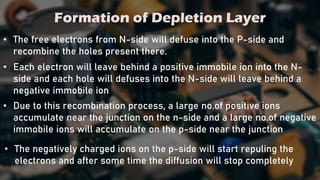
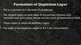
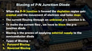
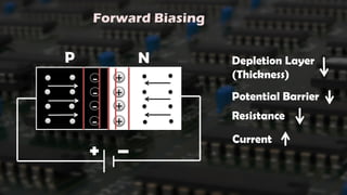
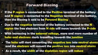
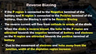
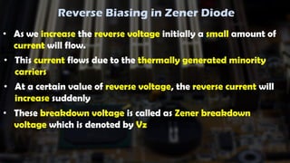
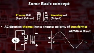
3) The formation and biasing of p-n junction diodes is explained, including the diffusion process that creates a depletion layer, and how forward and reverse biasing changes the width of this layer to allow or block current flow.