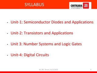
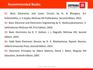
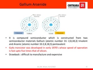
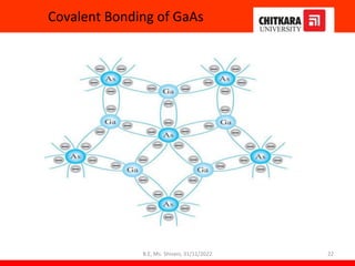
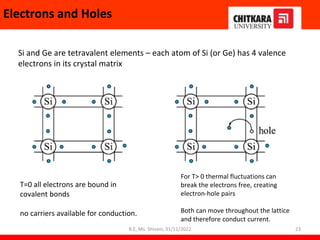
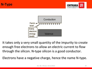
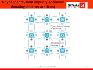
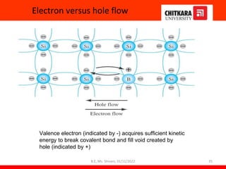
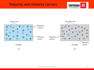
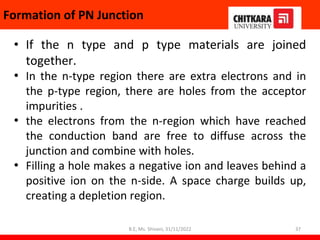
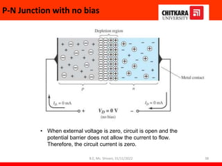
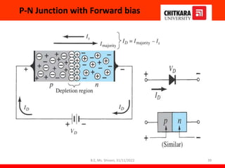
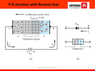
This document outlines the syllabus for the Basic Electronics course with code EC22001. The course covers 4 units: Semiconductor Diodes and Applications, Transistors and Applications, Number Systems and Logic Gates, and Digital Circuits. The introductory section provides an overview of electronics and semiconductor materials like silicon and gallium arsenide. It also discusses doping to alter conductivity and the formation of PN junctions in semiconductor devices. Recommended textbooks are listed for reference.
The MOSFET is an important element in embedded system design which is used to control the loads as per the requirement. The MOSFET is a high voltage controlling device provides some key features for circuit designers in terms of their overall performance.
A Kelvin bridge, also called a Kelvin double bridge and in some countries a Thomson bridge, is a measuring instrument used to measure unknown electrical resistors below 1 ohm. It is specifically designed to measure resistors that are constructed as four terminal resistors.
Ammeter, voltmeter, wattmeter, power factor meterHome
What is Ammeter, its working principle and its three Ammeter method. What is Voltmeter, working principle and three Voltmeter Method. Watt meter and its working principle.
The Basics of electronics can be studied also through the link http://bit.ly/2PPv0mv
A transformer is a passive electrical device that transfers electrical energy from one electrical circuit to one or more circuits.
The following presentation is a part of the level 4 module -- Electrical and Electronic Principles. This resources is a part of the 2009/2010 Engineering (foundation degree, BEng and HN) courses from University of Wales Newport (course codes H101, H691, H620, HH37 and 001H). This resource is a part of the core modules for the full time 1st year undergraduate programme.
The BEng & Foundation Degrees and HNC/D in Engineering are designed to meet the needs of employers by placing the emphasis on the theoretical, practical and vocational aspects of engineering within the workplace and beyond. Engineering is becoming more high profile, and therefore more in demand as a skill set, in today’s high-tech world. This course has been designed to provide you with knowledge, skills and practical experience encountered in everyday engineering environments.
Electronics part I- covers the definition of electronics, applications of electronics in real life situation, energy band theory and its use in differentiating insulators, semiconductors and conductors. There is clear illustrations of the concepts covered.
Introduction to Semiconductor Devices.
In modern world no other technology permeates every nook and cranny of our existence as does electronics.
Application of electronics are : Televisions, radios, stereo equipment, computers, scanners, electronic control systems (in cars for example) etc.
Industrial Training at Shahjalal Fertilizer Company Limited (SFCL)MdTanvirMahtab2
This presentation is about the working procedure of Shahjalal Fertilizer Company Limited (SFCL). A Govt. owned Company of Bangladesh Chemical Industries Corporation under Ministry of Industries.
Explore the innovative world of trenchless pipe repair with our comprehensive guide, "The Benefits and Techniques of Trenchless Pipe Repair." This document delves into the modern methods of repairing underground pipes without the need for extensive excavation, highlighting the numerous advantages and the latest techniques used in the industry.
Learn about the cost savings, reduced environmental impact, and minimal disruption associated with trenchless technology. Discover detailed explanations of popular techniques such as pipe bursting, cured-in-place pipe (CIPP) lining, and directional drilling. Understand how these methods can be applied to various types of infrastructure, from residential plumbing to large-scale municipal systems.
Ideal for homeowners, contractors, engineers, and anyone interested in modern plumbing solutions, this guide provides valuable insights into why trenchless pipe repair is becoming the preferred choice for pipe rehabilitation. Stay informed about the latest advancements and best practices in the field.
NO1 Uk best vashikaran specialist in delhi vashikaran baba near me online vas...Amil Baba Dawood bangali
Contact with Dawood Bhai Just call on +92322-6382012 and we'll help you. We'll solve all your problems within 12 to 24 hours and with 101% guarantee and with astrology systematic. If you want to take any personal or professional advice then also you can call us on +92322-6382012 , ONLINE LOVE PROBLEM & Other all types of Daily Life Problem's.Then CALL or WHATSAPP us on +92322-6382012 and Get all these problems solutions here by Amil Baba DAWOOD BANGALI
#vashikaranspecialist #astrologer #palmistry #amliyaat #taweez #manpasandshadi #horoscope #spiritual #lovelife #lovespell #marriagespell#aamilbabainpakistan #amilbabainkarachi #powerfullblackmagicspell #kalajadumantarspecialist #realamilbaba #AmilbabainPakistan #astrologerincanada #astrologerindubai #lovespellsmaster #kalajaduspecialist #lovespellsthatwork #aamilbabainlahore#blackmagicformarriage #aamilbaba #kalajadu #kalailam #taweez #wazifaexpert #jadumantar #vashikaranspecialist #astrologer #palmistry #amliyaat #taweez #manpasandshadi #horoscope #spiritual #lovelife #lovespell #marriagespell#aamilbabainpakistan #amilbabainkarachi #powerfullblackmagicspell #kalajadumantarspecialist #realamilbaba #AmilbabainPakistan #astrologerincanada #astrologerindubai #lovespellsmaster #kalajaduspecialist #lovespellsthatwork #aamilbabainlahore #blackmagicforlove #blackmagicformarriage #aamilbaba #kalajadu #kalailam #taweez #wazifaexpert #jadumantar #vashikaranspecialist #astrologer #palmistry #amliyaat #taweez #manpasandshadi #horoscope #spiritual #lovelife #lovespell #marriagespell#aamilbabainpakistan #amilbabainkarachi #powerfullblackmagicspell #kalajadumantarspecialist #realamilbaba #AmilbabainPakistan #astrologerincanada #astrologerindubai #lovespellsmaster #kalajaduspecialist #lovespellsthatwork #aamilbabainlahore #Amilbabainuk #amilbabainspain #amilbabaindubai #Amilbabainnorway #amilbabainkrachi #amilbabainlahore #amilbabaingujranwalan #amilbabainislamabad
Hierarchical Digital Twin of a Naval Power SystemKerry Sado
A hierarchical digital twin of a Naval DC power system has been developed and experimentally verified. Similar to other state-of-the-art digital twins, this technology creates a digital replica of the physical system executed in real-time or faster, which can modify hardware controls. However, its advantage stems from distributing computational efforts by utilizing a hierarchical structure composed of lower-level digital twin blocks and a higher-level system digital twin. Each digital twin block is associated with a physical subsystem of the hardware and communicates with a singular system digital twin, which creates a system-level response. By extracting information from each level of the hierarchy, power system controls of the hardware were reconfigured autonomously. This hierarchical digital twin development offers several advantages over other digital twins, particularly in the field of naval power systems. The hierarchical structure allows for greater computational efficiency and scalability while the ability to autonomously reconfigure hardware controls offers increased flexibility and responsiveness. The hierarchical decomposition and models utilized were well aligned with the physical twin, as indicated by the maximum deviations between the developed digital twin hierarchy and the hardware.
Student information management system project report ii.pdfKamal Acharya
Our project explains about the student management. This project mainly explains the various actions related to student details. This project shows some ease in adding, editing and deleting the student details. It also provides a less time consuming process for viewing, adding, editing and deleting the marks of the students.
Welcome to WIPAC Monthly the magazine brought to you by the LinkedIn Group Water Industry Process Automation & Control.
In this month's edition, along with this month's industry news to celebrate the 13 years since the group was created we have articles including
A case study of the used of Advanced Process Control at the Wastewater Treatment works at Lleida in Spain
A look back on an article on smart wastewater networks in order to see how the industry has measured up in the interim around the adoption of Digital Transformation in the Water Industry.
Cosmetic shop management system project report.pdfKamal Acharya
Buying new cosmetic products is difficult. It can even be scary for those who have sensitive skin and are prone to skin trouble. The information needed to alleviate this problem is on the back of each product, but it's thought to interpret those ingredient lists unless you have a background in chemistry.
Instead of buying and hoping for the best, we can use data science to help us predict which products may be good fits for us. It includes various function programs to do the above mentioned tasks.
Data file handling has been effectively used in the program.
The automated cosmetic shop management system should deal with the automation of general workflow and administration process of the shop. The main processes of the system focus on customer's request where the system is able to search the most appropriate products and deliver it to the customers. It should help the employees to quickly identify the list of cosmetic product that have reached the minimum quantity and also keep a track of expired date for each cosmetic product. It should help the employees to find the rack number in which the product is placed.It is also Faster and more efficient way.
3. SYLLABUS
• Unit-1: Semiconductor Diodes and Applications
• Unit-2: Transistors and Applications
• Unit 3: Number Systems and Logic Gates
• Unit-4: Digital Circuits
B.E, Ms. Shivani, 31/11/2022 3
4. Recommended Books
B1: Basic Electronics and Linear Circuits by N. N Bhargava, D.C
Kulshreshtha, S. C Gupta; McGraw Hill Publications, Second Edition, 2013.
B2: Basic Electrical and Electronics Engineering by R. Muthusubramanian, S.
Sahlivahanan McGraw Hill, First Edition, 2010.
B3: Basic Electronics by D. P. Kothari, I. J. Nagrath, McGraw Hill, Second
Edition, 2014.
B4: Solid State Electronic Devices by D. K. Bhattacharya, Rajnish Sharma,
Oxford University Press, Second Edition, 2013.
B5: Electronic Principles by Albert Malvino, David J. Bates, Mcgraw Hill
Education, Seventh Edition, 2007.
B.E, Ms. Shivani, 31/11/2022 4
5. Unit-1:
Semiconductor Diodes and Applications
• Introduction to Electronics, Familiarization with basic electronic components
and measuring instruments.
• Semiconductor Theory, Review of PN junction operation, Forward and Reverse
V-I Characteristics of PN-Junction Diode.
• Use of Diodes in Rectifiers, Half Wave, Full Wave-Centre-tap and Bridge
Rectifier (Circuit diagram, Waveforms, RMS value, DC value and Peak value,
PIV, Ripple Factor, Efficiency).
• Zener diode and its application as Voltage Regulator,
• Special Purpose Diodes: Light Emitting Diode (LED), Photodiode.
5
B.E, Ms. Shivani, 31/11/2022
7. Introduction to Electronics
● Electronics is that field of science and
engineering which deals with electronic
devices and their utilisation.
● Electron device is device in which conduction
takes place by the movement of electrons
through a vacuum, a gas or a semiconductor.
7
B.E, Ms. Shivani, 31/11/2022
12. Modern trends in Electronics
• Augmented and Virtual
Reality in Electronic
Manufacturing
• Robotics & Automation
• IoT Technology Driving
Smart Appliances
• Artificial Intelligence
12
B.E, Ms. Shivani, 31/11/2022
13. Miniaturization
• Modern Electronic devices now appear on wafers thousand of times
smaller than the single element of earlier networks.
13
B.E, Ms. Shivani, 31/11/2022
15. Semiconductors: Base of Electronics
Industry
• The construction of every electronic device
begins with semiconductor material of highest
quality.
• The semiconductors fall somewhere midway
between conductors and insulators.
• The three semiconductors used most
frequently in construction of electronic
devices are Ge, Si and GaAs
15
B.E, Ms. Shivani, 31/11/2022
17. Germanium (atomic number 32:
2,8,18,4)
• It has four valence electrons so known as tetravalent.
• It was relatively easy to find and was available in fairly large
quantities.
• Easy to refine to obtain high levels of purity
• Ge was first semiconductor to be used to construct Diode in 1939
and transistor in 1947
Drawback:
• It has low level of reliability due to its sensitivity to changes in
temperature
17
B.E, Ms. Shivani, 31/11/2022
18. Silicon (atomic number 14: 2,8,4)
• It has four valence electrons so known as tetravalent.
• It is better than germanium due to its less temperature sensitivity
and it is one of the most abundant material on earth.
• So it becomes leading semiconductor material for electronic
components and ICs
• In 1954, First silicon transistor was introduced
18
B.E, Ms. Shivani, 31/11/2022
20. Growing demands of Industry
• The field of electronics became increasingly
sensitive to issues of speed.
• Computers were operating at higher and higher
speeds
• Communication systems were operating at
higher levels of performance.
• So new semiconductor material was required
20
B.E, Ms. Shivani, 31/11/2022
21. Gallium Arsenide
• It is compound semiconductor which is constructed from two
semiconductor materials Gallium (atomic number 31: 2,8,18,3) trivalent
and Arsenic (atomic number 33:2,8,18,5) pentavalent
• GaAs transistor was developed in early 1970’s whose speed of operation
is fast upto five times that of silicon.
• Drawback : difficult to manufacture and expensive
21
B.E, Ms. Shivani, 31/11/2022
23. Si and Ge are tetravalent elements – each atom of Si (or Ge) has 4 valence
electrons in its crystal matrix
T=0 all electrons are bound in
covalent bonds
no carriers available for conduction.
For T> 0 thermal fluctuations can
break the electrons free, creating
electron-hole pairs
Both can move throughout the lattice
and therefore conduct current.
Electrons and Holes
B.E, Ms. Shivani, 31/11/2022 23
24. Intrinsic Material
A pure semiconductor crystal with no impurities or lattice defects is called an
intrinsic semiconductor.
• At T=0 K, No charge carriers.
• Valence band is filled with
electrons.
• Conduction band is empty.
• At T>0, Electron-hole pairs are
generated.
• EHPs are the only charge
carriers in intrinsic material.
• Since electron and holes are
created in pairs – the electron
concentration in conduction band, n
(electron/cm3) is equal to the
concentration of holes in the
valence band, p (holes/cm3).
• Each of these intrinsic carrier
concentrations is denoted ni.
Thus for intrinsic materials n=p=ni
Electron-hole pairs in the covalent
bonding model in the Si crystal.
B.E, Ms. Shivani, 31/11/2022 24
25. Intrinsic Silicon
At any temperature above absolute zero temperature, there
is a finite probability that an electron in the lattice will be
knocked loose from its position.
B.E, Ms. Shivani, 31/11/2022 25
26. Intrinsic carriers and relative mobility
• The free electrons in a material due to
external causes are known as intrinsic carriers.
• Number of intrinsic carriers in popular
semiconductors are arranged in descending
order as Ge>GaAs>Si (as per the internal
properties)
• But electronic devices have fast response time
due to maximum relative mobility of free
carriers
• Order of relative mobility is GaAs>Ge>Si 26
B.E, Ms. Shivani, 31/11/2022
28. • Another way to increase the number of
charge carriers is to add them in from an
external source.
• Doping or implant is the term given to a
process whereby one element is injected with
atoms of another element in order to change
its properties.
• Semiconductors (Si or Ge) are typically doped
with elements such as Boron, Arsenic and
Phosphorous to change and enhance their
electrical properties. 28
Increasing conductivity by doping
B.E, Ms. Shivani, 31/11/2022
29. Effect of donor impurity on energy band
structure
29
B.E, Ms. Shivani, 31/11/2022
31. P-Type
The absence of an electron creates the effect of a positive
charge, hence the name P-type.
Holes can conduct current. A hole happily accepts an
electron from a neighbor, moving the hole over a space. P-
type silicon is a good conductor.
B.E, Ms. Shivani, 31/11/2022 31
32. P type (trivalent impurity boron
accepting electron from silicon)
32
B.E, Ms. Shivani, 31/11/2022
33. N-Type
It takes only a very small quantity of the impurity to create
enough free electrons to allow an electric current to flow
through the silicon. N-type silicon is a good conductor.
Electrons have a negative charge, hence the name N-type.
B.E, Ms. Shivani, 31/11/2022 33
34. N type (pentavalent impurity Antimony
donating electron to silicon)
34
B.E, Ms. Shivani, 31/11/2022
35. Electron versus hole flow
35
Valence electron (indicated by -) acquires sufficient kinetic
energy to break covalent bond and fill void created by
hole (indicated by +)
B.E, Ms. Shivani, 31/11/2022
37. Formation of PN Junction
• If the n type and p type materials are joined
together.
• In the n-type region there are extra electrons and in
the p-type region, there are holes from the acceptor
impurities .
• the electrons from the n-region which have reached
the conduction band are free to diffuse across the
junction and combine with holes.
• Filling a hole makes a negative ion and leaves behind a
positive ion on the n-side. A space charge builds up,
creating a depletion region.
37
B.E, Ms. Shivani, 31/11/2022
38. P-N Junction with no bias
• When external voltage is zero, circuit is open and the
potential barrier does not allow the current to flow.
Therefore, the circuit current is zero.
B.E, Ms. Shivani, 31/11/2022 38
40. P-N Junction with Forward bias
• When P-type (Anode is connected to +ve terminal and n- type
(cathode) is connected to –ve terminal of the supply voltage,
is known as forward bias.
• The potential barrier is reduced when diode is in the
forward biased condition.
• At some forward voltage, the potential barrier altogether
eliminated and current starts flowing through the diode and
also in the circuit. The diode is said to be in ON state.
• The current increases with increasing forward voltage.
40
B.E, Ms. Shivani, 31/11/2022
42. P-N Junction with Reverse bias
• When N-type (cathode) is connected to +ve terminal
and P-type (Anode) is connected to the –ve terminal
of the supply voltage is known as reverse bias and
the potential barrier across the junction increases.
• Therefore, the junction resistance becomes very high
and a very small current (reverse saturation current)
flows in the circuit. The diode is said to be in OFF
state.
• The reverse bias current is due to minority charge
carriers.
42
B.E, Ms. Shivani, 31/11/2022
43. Important Definitions
• Knee Voltage
The voltage is applied then the junction starts increasing rapidly. It
is known as knee voltage and an alternate name of this is cut in voltage.
• Breakdown Voltage
The minimum reverse voltage that makes the diode conduct
appreciably in reverse.
• Peak Inverse Voltage
The maximum voltage a diode or other device can withstand in the
reverse-biased direction before breakdown.
• Maximum Power Rating
Maximum power that a PN junction or diode can dissipate
without damaging the device itself.
B.E, Ms. Shivani, 31/11/2022 43
44. Jargons
▪ Knee Voltage
▪ Breakdown Voltage
▪ Maximum Forward Current
▪ Peak Inverse Voltage
▪ Maximum Power Rating
V-I Characteristics
1. Forward Bias Characteristics
2. Reverse Bias Characteristics
B.E, Ms. Shivani, 31/11/2022 44
45. Jargons
▪ Knee Voltage
▪ Breakdown Voltage
▪ Maximum Forward Current
▪ Peak Inverse Voltage
▪ Maximum Power Rating
1. Forward Bias Characteristics
2. Reverse Bias Characteristics
V-I Characteristics
B.E, Ms. Shivani, 31/11/2022 45
46. Jargons
▪ Knee Voltage
▪ Breakdown Voltage
▪ Maximum Forward Current
▪ Peak Inverse Voltage
▪ Maximum Power Rating
V-I Characteristics
B.E, Ms. Shivani, 31/11/2022 46
47. Equivalent Circuits
PIECEWISE-LINEAR
MODEL
SIMPLIFIED MODEL IDEAL DIODE
Rnetwork » Rav
Rnetwork » Rav
Enetwork » VT
CONDITION
TYPE
MODEL
CHARACTERISTICS
Id
Vd
Id
Vd
Id
Vd
o o o
rav
VT VT
Ideal
Diode
Ideal
Diode
Ideal
Diode
VT VT
rav
B.E, Ms. Shivani, 31/11/2022 47