Electron Devices-14EC2002
COURSE CONTENTS
Semiconductor in Equilibrium: Charge carriers in
semiconductors, Extrinsic semiconductors-Charge
neutrality, position of Fermi energy level-carrier transport
phenomena-Carrier generation and recombination-
Continuity equation –Quasi Fermi energy levels-PN
junctions : basic structure, applied bias- PN junction
diode : PN junction current, small signal model of the PN
junction-BJT: Bipolar transistor action, Ebers moll model-
static characteristics of transistors – JFET : JFET
concepts, JFET characteristics – MOSFET : structure
and Characteristics – UJT –SCR - DIAC – TRIAC-Zener
diode – Tunnel diodes– LED.
Silicon
Nucleus
Valence Band
Energy Bands
(Shells)
Si has 14 Electrons
Silicon is the primary semiconductor used in VLSI systems
At T=0K, the
highest energy
band occupied by
an electron is
called the valence
band.
Silicon has 4 outer shell /
valence electrons
Energy Bands
Valence Band
Conduction Band
Energy
Bandgap
Eg
EC
EV
Last filled energy
band at T=0K
First unfilled energy
band at T=0K
Band Diagrams
Eg
EC
EV
Band Diagram Representation
Energy plotted as a function of position
EC  Conduction band
 Lowest energy state for a free electron
EV  Valence band
 Highest energy state for filled outer shells
EG  Band gap
 Difference in energy levels between EC and EV
 No electrons (e-) in the bandgap (only above EC or below EV)
 EG = 1.12eV in Silicon
Increasing electron energy
Conductor, Semiconductor or Insulator?
Conductor Semiconductor Insulator
Examples
Silver
Copper
Gold
Silicon
Si/Ge
SiO2
Diamond
Overlapping Bands
Intrinsic Semiconductor
Silicon has 4 outer shell /
valence electrons
Forms into a lattice structure
to share electrons
Intrinsic Silicon
EC
EV
The valence band is full, and
no electrons are free to move
about
However, at temperatures
above T=0K, thermal energy
shakes an electron free
Semiconductor Properties
For T > 0K
Electron shaken free and can
cause current to flow
e–
h+
• Generation – Creation of an electron (e-)
and hole (h+) pair
• h+ is simply a missing electron, which
leaves an excess positive charge (due to
an extra proton)
• Recombination – if an e- and an h+ come
in contact, they annihilate each other
• Electrons and holes are called “carriers”
because they are charged particles –
when they move, they carry current
• Therefore, semiconductors can conduct
electricity for T > 0K … but not much
current (at room temperature (300K), pure
silicon has only 1 free electron per 3
trillion atoms)
Doping
• Doping – Adding impurities to the silicon
crystal lattice to increase the number of
carriers
• Add a small number of atoms to increase
either the number of electrons or holes
Periodic Table
Column 4
Elements have 4
electrons in the
Valence Shell
Column 3
Elements have 3
electrons in the
Valence Shell
Column 5
Elements have 5
electrons in the
Valence Shell
Donors n-Type Material
Donors
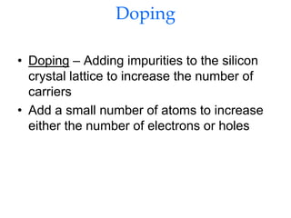
• Add atoms with 5 valence-band
electrons
• ex. Phosphorous (P)
• “Donates” an extra e- that can freely
travel around
• Leaves behind a positively charged
nucleus (cannot move)
• Overall, the crystal is still electrically
neutral
• Called “n-type” material (added
negative carriers)
• ND = the concentration of donor
atoms [atoms/cm3 or cm-3]
~1015-1020cm-3
• e- is free to move about the crystal
(Mobility mn ≈1350cm2/V)
+
Acceptors Make p-Type Material
––
h+
Acceptors
• Add atoms with only 3 valence-
band electrons
• ex. Boron (B)
• “Accepts” e– and provides extra h+
to freely travel around
• Leaves behind a negatively
charged nucleus (cannot move)
• Overall, the crystal is still
electrically neutral
• Called “p-type” silicon (added
positive carriers)
• NA = the concentration of acceptor
atoms [atoms/cm3 or cm-3]
• Movement of the hole requires
breaking of a bond! (This is hard,
so mobility is low, μp ≈ 500cm2/V)
SEMICONDUCTOR DEVICES

Inroduction 03.07

  • 1.
  • 2.
    COURSE CONTENTS Semiconductor inEquilibrium: Charge carriers in semiconductors, Extrinsic semiconductors-Charge neutrality, position of Fermi energy level-carrier transport phenomena-Carrier generation and recombination- Continuity equation –Quasi Fermi energy levels-PN junctions : basic structure, applied bias- PN junction diode : PN junction current, small signal model of the PN junction-BJT: Bipolar transistor action, Ebers moll model- static characteristics of transistors – JFET : JFET concepts, JFET characteristics – MOSFET : structure and Characteristics – UJT –SCR - DIAC – TRIAC-Zener diode – Tunnel diodes– LED.
  • 3.
    Silicon Nucleus Valence Band Energy Bands (Shells) Sihas 14 Electrons Silicon is the primary semiconductor used in VLSI systems At T=0K, the highest energy band occupied by an electron is called the valence band. Silicon has 4 outer shell / valence electrons
  • 4.
    Energy Bands Valence Band ConductionBand Energy Bandgap Eg EC EV Last filled energy band at T=0K First unfilled energy band at T=0K
  • 5.
    Band Diagrams Eg EC EV Band DiagramRepresentation Energy plotted as a function of position EC  Conduction band  Lowest energy state for a free electron EV  Valence band  Highest energy state for filled outer shells EG  Band gap  Difference in energy levels between EC and EV  No electrons (e-) in the bandgap (only above EC or below EV)  EG = 1.12eV in Silicon Increasing electron energy
  • 6.
    Conductor, Semiconductor orInsulator? Conductor Semiconductor Insulator Examples Silver Copper Gold Silicon Si/Ge SiO2 Diamond Overlapping Bands
  • 7.
    Intrinsic Semiconductor Silicon has4 outer shell / valence electrons Forms into a lattice structure to share electrons
  • 8.
    Intrinsic Silicon EC EV The valenceband is full, and no electrons are free to move about However, at temperatures above T=0K, thermal energy shakes an electron free
  • 9.
    Semiconductor Properties For T> 0K Electron shaken free and can cause current to flow e– h+ • Generation – Creation of an electron (e-) and hole (h+) pair • h+ is simply a missing electron, which leaves an excess positive charge (due to an extra proton) • Recombination – if an e- and an h+ come in contact, they annihilate each other • Electrons and holes are called “carriers” because they are charged particles – when they move, they carry current • Therefore, semiconductors can conduct electricity for T > 0K … but not much current (at room temperature (300K), pure silicon has only 1 free electron per 3 trillion atoms)
  • 10.
    Doping • Doping –Adding impurities to the silicon crystal lattice to increase the number of carriers • Add a small number of atoms to increase either the number of electrons or holes
  • 11.
    Periodic Table Column 4 Elementshave 4 electrons in the Valence Shell Column 3 Elements have 3 electrons in the Valence Shell Column 5 Elements have 5 electrons in the Valence Shell
  • 12.
    Donors n-Type Material Donors •Add atoms with 5 valence-band electrons • ex. Phosphorous (P) • “Donates” an extra e- that can freely travel around • Leaves behind a positively charged nucleus (cannot move) • Overall, the crystal is still electrically neutral • Called “n-type” material (added negative carriers) • ND = the concentration of donor atoms [atoms/cm3 or cm-3] ~1015-1020cm-3 • e- is free to move about the crystal (Mobility mn ≈1350cm2/V) +
  • 13.
    Acceptors Make p-TypeMaterial –– h+ Acceptors • Add atoms with only 3 valence- band electrons • ex. Boron (B) • “Accepts” e– and provides extra h+ to freely travel around • Leaves behind a negatively charged nucleus (cannot move) • Overall, the crystal is still electrically neutral • Called “p-type” silicon (added positive carriers) • NA = the concentration of acceptor atoms [atoms/cm3 or cm-3] • Movement of the hole requires breaking of a bond! (This is hard, so mobility is low, μp ≈ 500cm2/V)
  • 14.