Downloaded 231 times

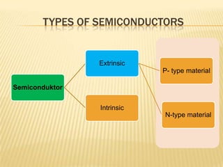


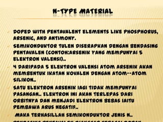


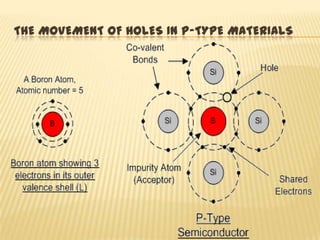


1) Semiconductors exhibit characteristics between conductors and insulators. Diodes and transistors are early components made from semiconductors. 2) There are two types of semiconductors - intrinsic and extrinsic. Intrinsic semiconductors do not contain any foreign atoms while extrinsic are created by diffusing or implanting impurities into intrinsic semiconductors. 3) Extrinsic semiconductors can be n-type or p-type depending on the impurity used - n-type uses elements like phosphorus that add free electrons, while p-type uses elements like boron that create holes. The combination of n-type and p-type materials creates the PN