Downloaded 445 times
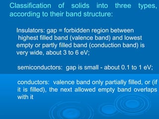


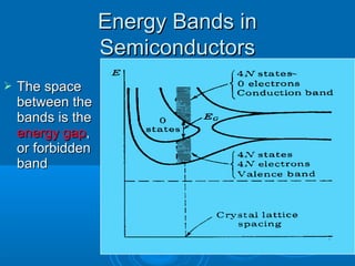
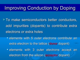
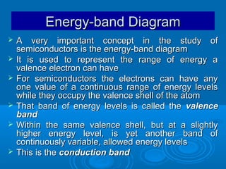
![Band Gap
Between
the valence and the conduction
band is a range of energy levels where there
are no allowed states for an electron
This is the band gap E G
In silicon at room temperature [in electron
.
volts]: E G = 11 eV
Electron volt is an atomic measurement
unit, 1 eV energy is necessary to decrease of
the potential of the electron with 1 V.
1eV = 1.602 × 10 −19 joule](https://image.slidesharecdn.com/semiconductors-131025091621-phpapp02/85/Semiconductors-27-320.jpg)


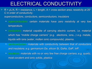
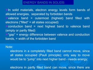
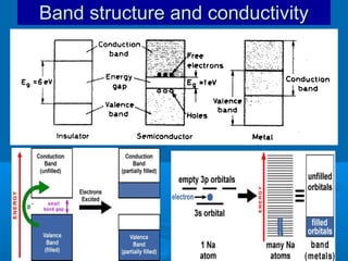
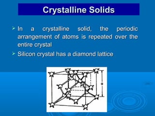
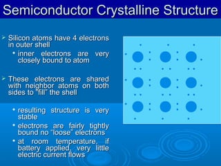
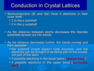
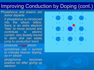
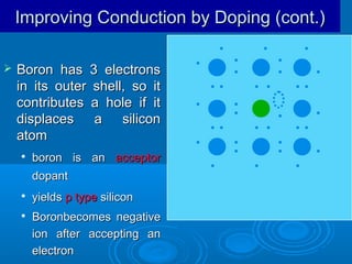
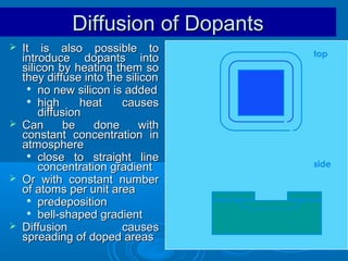
This document discusses solids and semiconductor devices. It begins by explaining the electrical conductivity of different materials like conductors, semiconductors, and insulators. It then describes the energy band structure of solids, noting that semiconductors have a small band gap between the valence and conduction bands. The document discusses intrinsic and doped semiconductors, including n-type and p-type materials. It also covers diodes, p-n junctions, and how they function when forward and reverse biased. Key concepts covered include band theory, hole-electron pairs, and improving conductivity through doping.


