Quantum dots are tiny semiconductor crystals between 2-10 nanometers in size. Their properties depend on factors like size and energy levels. Smaller quantum dots emit higher frequency/shorter wavelength blue light while larger dots emit lower frequency/longer wavelength red light. Quantum dots have potential applications in solar cells, displays, and medical imaging due to their tunable light emission and other optical properties. They are typically made through colloidal synthesis which allows for mass production under mild conditions.
This includes what is Quantum Dots and their properties ,types of synthesis methods of nano materials such as top down, bottom up etc.It includes few things about Carbon Quantum Dots.
Quantum dots (QD) are semiconductors made via several possible routes. John Ashmead discusses how they are made, their properties and their applications in research.
Quantum Dot-sensitized Solar Cells: A ReviewjournalBEEI
Quantum dot-sensitized solar cell (QDSSC) has an analogous structure and working principle to the dye sensitizer solar cell (DSSC). It has drawn great attention due to its unique features, like multiple exciton generation (MEG), simple fabrication and low cost. The power conversion efficiency (PCE) of QDSSC is lower than that of DSSC. To increase the PCE of QDSSC, it is required to develop new types of working electrodes, sensitizers, counter electrodes and electrolytes. This review highlights recent developments in QDSSCs and their key components, including the photoanode, sensitizer, electrolyte and counter electrode.
Doping the quantum dots is one of the most emerging hot topics. In addition to the enhancement of the optical properties of the quantum dots, it also improve the chemical stability and inhibit the self quenching effect in the undoped quantum dots. In addition to that, It opened the field of using non Cadmium based quantum dots, that will be very useful for various biological applications.
Quantum Dot Light Emitting Diode
Introduction
Quantum dots (QD) or semiconductor Nano crystals could provide an alternative for commercial applications such as display technology. This display technology would be similar to organic light-emitting diode (OLED) displays, in that light would be supplied on demand, which would enable more efficient displays.
Quantum dots could support large, flexible displays. At present, they are used only to filter light from LEDs to backlight LCDs, rather than as actual displays. Properties and performance are determined by the size and/or composition of the QD. QDs are both photo-active (photo luminescent) and electro-active (electroluminescent) allowing them to be readily incorporated into new emissive display architectures.
Definition
QD-LED or QLED is considered as a next generation display technology after OLED-Displays.
“QLED means Quantum dot light emitting diodes and are a form of light emitting technology and consist of nano-scale crystals that can provide an alternative for applications such as display technology”. The light emitting centers are cadmium selenide (CdSe) nanocrystals, or quantum dots.
Charactristics
❀ QLEDs are a reliable, energy efficient, tunable color solution for display and lighting applications that reduce manufacturing costs, while employing ultra-thin, transparent or flexible materials.
❀ Quantum-dot-based LEDs are characterized by pure and saturated emission colors with narrow bandwidth.
❀ Their emission wavelength is easily tuned by changing the size of the quantum dots. Moreover, QD-LED offer high color purity and durability combined with the efficiency, flexibility, and low processing cost of organic light-emitting devices. QD-LED structure can be tuned over the entire visible wavelength range from 460 nm (blue) to 650 nm
❀ Due to spectrally narrow, tunable emission, and ease of processing, colloidal QDs are attractive materials for LED technologies.
This presentation contains a basic introduction to quantum dots,their discovery, properties, applications,advantages,limitations and future prospects.It also contains a brief overview of experimental work carried out and results obtained during my summer term project.
Quantum dots were discovered in solids (glass crystals) in 1980 by Russian physicist Alexei Ekimov while working at the Vavilov State Optical Institute. In late 1982, American chemist Louis E. Brus, then working at Bell Laboratories (and now a professor at Columbia University), discovered the same phenomenon in colloidal solutions (where small particles of one substance are dispersed throughout another; milk is a familiar example). These two scientists shared the Optical Society of America's 2006 R.W. Wood Prize for their pioneering work.
Nanotechnology in Semiconductor Nanostructure.
Presentation on "Quantum Dot", was performed under the Subject "QUANTUM PHENOMENA IN NANOSTRUCTURES" at AIUB. The simulation is done from a website nanoHUB which stands for online simulation for nanotechnology- https://nanohub.org/
know more about nanomaterials and its apllication in future as well as current situation, and what wil we reserch on basis of nanomaterials and carbon structure and its aplication in such futuriastic manner.
Nanocrystals called quantum dots have a range of optical and magnetic properties that make them useful in various applications. Learn more about quantum dots from us.
1. Title
QUANTUM DOTS: - Introduction & Experiments
Name: - Aakash Chandrakant Mhankale
CWID: - 803000470
======================================================
Introduction:-
Quantum dots are tiny semiconductor crystals this means these can conduct or resist depending upon
the temperature and impurity of the semiconductor. Quantum dots ranges is from 2 to 10 Nano meters.
Because of the size of the physics is governed by the quantum mechanics.
Important properties of quantum dots depends on the following factors: -
Size, Energy Levels
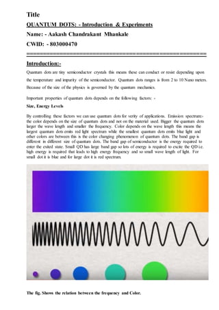
By controlling these factors we can use quantum dots for verity of applications. Emission spectrum:-
the color depends on the size of quantum dots and not on the material used. Bigger the quantum dots
larger the wave length and smaller the frequency. Color depends on the wave length this means the
largest quantum dots emits red light spectrum while the smallest quantum dots emits blue light and
other colors are between this is the color changing phenomenon of quantum dots. The band gap is
different in different size of quantum dots. The band gap of semiconductor is the energy required to
enter the exited state. Small QD has large band gap so lots of energy is required to excite the QD i.e.
high energy is required that leads to high energy frequency and so small wave length of light. For
small dot it is blue and for large dot it is red spectrum.
The fig. Shows the relation between the frequency and Color.
2. Optical properties
In case of semiconductors, when light gets absorbed it generally tends an electron gets excited from
valence to the conduction band, hole is left behind. Exciton recombines the excitons energy is emitted
as light, this phenomenon is called Fluorescence. In simple words, the energy produced because of the
emitted photon is equal to addition of the band gap energy between the highest level and the lowest
energy level.
Confinement energy directly depends on the quantum dots size, absorption & fluorescence emission
tuned by changing the size of the quantum dot. If the dot is larger it is reddish (i.e.lower energy) its
absorption and fluorescence colour spectrum. Contrariwise, smaller dots absorb and emit bluer (i.e.
higher energy) light. Further, the lifetime of fluorescence is determined by the size of the quantum dot.
Larger dots are closely spaced. So, electron-hole pairs in larger dots live longer producing larger dots
to show a longer lifetime.
For enlightening fluorescence quantum, quantum dots are invented that has larger bandgap
semiconductor material around them.
Band gap energy
Where ab is the, m is the mass, and εr is the size-dependent dielectric constant (Relative
permittivity), Bohr radius=0.053 nm, μ is the reduced mass,
3. Why Quantum Dots?
Unique properties of QD are used in the many applications such as
Medical imaging, light emitting displays, photovoltaic cells. QD includes electrical and nonlinear
optical properties. These properties are partly result of high surface to volume ration. The properties
make QD important for the electronics industry.
• The average distance between an electron and a hole in an exciton is called the Excited Bohr
Radius.
• When the size of the semiconductor falls below the Bohr Radius, the semiconductor is called a
quantum dot.
Quantum dots can be simulated by the Ultra Violate rays or electricity. This property makes QD ideal
for using solar cell. The verity in size of quantum dots used to synthesize the solar cell which results in
greater energy absorption. The photons from the light travels into the cell and striking the quantum
dots particles which will raise the energy of electrons in the quantum dots. Electrons will get injected
into titanium dioxide and travel through it to the conductive surface of the electrodes and leave holes
in the quantum dots. Quantum dots takes electrons from electrolyte and the electron deleted electrolyte
in turn takes electron from the counter electrode and this will create a voltage across the cell.
Theoretically, this could boost solar power efficiency from 20-30% to as high as 65%.
So in short, the appropriate area of the solar spectrum absorbs the sunlight and it will tune the band
gap of the semiconductor. Further by tuning the size of QD it allows the engineers to enhance the
performance of the device. As the performance of the device is increasing by the process then it is the
low cost and high-performance devices will make a high impact in energy conversion industry across
the world.
Quantum dots used in vivid colour efficient display. Some companies are already working on it and
used for flexible screen and vibrant colours. Quantum Dots are used in medical images for high
clarity, but still lot of research to be done to see QD as a medical use.
• Medical Imaging: -
• Quantum Dots are useful for monitoring cancerous cells and provides a way to find out the root
cause of the cancer.
• QDs are much more resistant to degradation than other optical imaging probes such as organic
dyes, allowing them to track cell processes for longer periods of time.
4. Quantum Dots in Television Industry
Conventional TV:
Standard LED has a blue backlight and on it has yellow layer of phosphate added to them which make
the blue light to change from blue to white. Further, it is filtered through red, green and blue sub pixels
at varying intensity and creating pixels in entire area but the performance of white light for Red colour
is not that good this is where the Quantum Dots LCD comes into the picture.
Quantum dots Liquid Crystal Display also uses blue as a back light but instead of using yellow
phosphate layer to create white light it uses green n red Nano particles which are from 1 to 4nm and
they actually emits light rather than just filtering. The blue backlight mixes with the Green and Red to
make more bright and clear white light and it efficiently passed thought sub pixels to filter, which
allow engineers to create screens which require less operational energy to achieve more vibrant
colours. AS QDLCD operates at low energy cost the production companies are interested in this
technology. As the cost of QDLCD is ½ or 1/3rd of the OLED TVs.
What are the benefits of quantum dots in Television industry?
The tune ability of QDs gives them the ability to emit nearly any frequency of light - a traditional LED
lacks this ability.
Higher peak brightness
Better colour accuracy: - The light produced by QD is closely tied with size so that they can accurately
emit the exact kind of light which is required.
Higher colour saturation: - On OLED screen the colours will “pop” more due to huge colour gamut
OLED screen whereas the quantum dots can increase the colour gamut on LCD screen by 40 to 50%.
What are the downsides of quantum dots?
As there are many difficulties in integrating quantum dots into screen from users point of view there is
only one downside seen so far but it is serious the issue is light bleed issue. The reader on kindle HDX
which was 1st quantum dots tablet the content was not visible in many condition. It was bleeding blue
light instead of white because the backlight is blue in QD. Solving this issue is very important as the
money factor is involved in this. Apple is currently working on solution.
5. “Nanocrystal displays are 30% more in visible spectrum and using only 335 to 60% less power than
LCDs. Further, blue quantum dots require timing control during the reaction, because blue quantum
dots are somewhat above the minimum size. Sunlight contains approx. equal luminosities of red, green
and blue, a display needs to harvest approximately equal luminosities of red, blue and green.
How quantum dots are made?
Colloidal Synthesis: This method can be used to create large numbers of quantum dots all at once.
Additionally, it is the cheapest method and is able to occur at non-extreme conditions.
Electron-Beam Lithography: A pattern is etched by an electron beam device and the semiconducting
material is deposited onto it.
• Electrons are accelerated out of an electron gun and sent through condenser lens optics directly
onto a wafer. λ = (12.3 Å / √V).
• Disadvantage(s):
• The lithography is serial (masks aren’t used; instead the beam itself sweeps across the wafer)
Comparatively it has low throughput ~5 wafers per hour at less than 1 micrometer resolution
• The proximity effect: Electrons scatter because they are relatively low in mass, reducing the
resolution.
• Molecular Beam Epitaxy: Molecular beam epitaxy (MBE) is the deposition of one or more
pure materials onto a single crystal wafer one layer of atoms at a time in order to form a perfect
6. crystal. A thin layer of crystals can be produced by heating the constituent elements separately
until they begin to evaporate; then allowing them to collect and react on the surface of a wafer.
MBE system consist of:
• a growth chamber
• a vacuum pump
• a effusion (Knudsen) cells
• a manipulator and substrate heater
• an in-situ characterization tool – RHEED
(reflection high energy electron diffraction)
Generally the quantum dots are prepared by the chemical reaction in solution resulting in solid Nano
crystals. Chemicals combined to heat at 255 C the more the reaction time it will affects the size of the
crystal. As soon as the mixture is out of the heat the particles will retain their size and color.
Many semiconductor materials can be used to create Quantum Dots. For example
Cadmium Selenide, Lead Selenide, Indium Arsenic
Cadmium Sulfide , Lead Sulfide, Indium Phosphorus
But, these are the heavy metals and potentially dangerous for the health which limits the use of
Quantum Dots Technology.
The promising option for this is use of coper sulfide / zinc sulfide for protecting coating.
How do Quantum Dots work?
QCA Basics (quantum-dotcellularautomata(QCA) cell):
Cells are basic elements of QCA. Each cell describes a bit with some charge.
• QCA CELLS CAN ONLY BE FOUND IN TWO STATES (LOGIC ‘0’ AND ‘1’)
7. As shown in the picture, it has 4 metal
conductors which is quantum dots. 4 dots of
QCA cell with one electron in with two of the
dots and mostly settled diagonally opposite
because the coulomb repulsion is less.
Electron can pass through tunnel junction but
they are not allowed to leave the cell.
We can change the logic state of the cell just by applying the –ve potential to the corner where the
quantum dot has electron. Because of this the next cell changes the state to lower the coulomb
repulsion. The above figure shows the logic-1 and logic-0 due to coulomb repulsion. That’s why to
carry information from one end to other only one position change of electron is sufficient unlike
CMOS where transfer of charge is required end to end.
The above figure shows that when you are applying 0 input the output is 1. This shows that this pattern
is implementing the Invertor logic.
8. Today’s digital technology the logic gates are driven by the voltages and the information in QCA is
defined by the position of electrons within the dots. The output cell should be at 45 degree from the 2
logic inputs to realize the invertor logic.
QCA Wire:-
• By placing two “cells” together and forcing the first cell into a certain state, the second cell
will assume the same state in order to lower its energy.
The diagram shows that the net output effect “1” is moved
on to the next cell.
By placing cells near to each other as shown “pseudo-wire”
so signal can transport from one end to other.
Majority gate M (A, B, C) = AB + BC + AC
When C selected as 0 will act as a AND gate M (A, B, 0) = AB and if C =1 then M (A, B, 1) = A+B.
A majority gate requires the same number of cells in QCA as an AND gate & OR gate. This is
contrasted with MOSFET technology (where the number of transistors required to realize a 3-input
majority gate is much more than that required for some other gates).
Clocking in QCA-Role and Types
Clocking is applying an appropriate voltage to a cell it leads to adjustment of tunnelling barriers so
that the electrons can transfer from one end to other. There can be a case where the cell be in
metastable state so the clocking play an important role in this scenario.
9. Shows clocking of a QCA cell. Here Vc means
clock voltage is applied. Clocking is performed in
one of two ways: zone clocking and continuous
clocking. In zone clocking, each QCA cell is
clocked using a four-phase clocking scheme as
shown in below figure. The four phases correspond
to switch, hold, release and relax.
In the switch phase,
Cells begin un-polarized and with low potential
barriers but the barriers are raised during this phase.
In the hold phase, the barriers are held high while in
the release phase, the barriers are lowered.
In the last phase, namely relax, the barriers remain
lowered and keep the cells in an un-polarized state.
An alternative to zone clocking is continuous
clocking, involves generation of a potential field by
a system of submerged electrodes.
The main difference between circuit design in QCA and that in conventional CMOS technology is that
a circuit in QCA has no control over the clocks contrasting in CMOS.
Hence, information is only transmitted through each cell and not retained. Each cell “erases” its own
state through every clock cycle. Further, every logic element in a QCA circuit is clocked.
When we rotate dots at 45 degree, the cells will act inversely. So, the wire created by this type of
pattern is called as “inversion chain” where each cell in the chain takes on the opposite polarization of
its nearest neighbours.
• Both dots are assumed to be identical but in reality, the upper dot is ~ 10% larger than
the lower one
Bound Exciton Energy
Quantum Dots
ny
nz
nx
10. Between positive and negative charged electrons there is always a coulomb attraction. Negative
energy involved in this is inversely proportional to the square of the size-dependent dielectric constant
and directly proportional to the Rydberg’s energy. If the size of the crystal is small than the exciton
Bohr radius then the coulomb interaction must be modified as per the condition.
So, these energies can be represented as: -
Where me is the free electron mass, mh is the hole mass, εr is the size-dependent dielectric constant,
a is the radius, μ is the reduced mass,
Quantum Dots energy is dependent on the size due to confinement effects.
Other Quantum Confined semiconductors are: -
1) Quantum Wells: - in which electrons or holes are in one dimension and allow free propagation
in 2 dimension.
2) Quantum Wire: - electrons or holes are in the 2 spatial dimension and allow free propagation in
the 3rd dimension.
Successful Switch between cells
For successful switch between the cell the
energy should be equal to or greater that Ekink.
Where Ekink= =Amount of Energy Required
for Successful Transmission
If the energy is less than the given equation then the cell may get into the metastable state.
The minimum difference in energy between the electron and hole is not simply the band gap, but the
energy difference between the n=1 energy state of the hole in the valence band, and the n=1 energy
state of the electron in the conduction band. This difference is equal to the quantum well energy
equation for the electron, plus the quantum well energy equation for the hole, plus the material band
gap energy.
k
k
n
kx
nz
ny
11. QCA Conclusions: -
• QCA is the most suitable successor to the CMOS VLSI system because of the advantages
mentioned before.
• The QCA technology is very useful in the future for developing of the processors and ASICs
that can be used for the general purpose or real time computing requirement.
• QCA will be the problem solver in the next coming era which will solve many problems in
electronic industry.
NECESSITY OF QUANTUM DOTS: LIMITATIONS OF CURRENT CMOS BASED
TECHNOLOGY
● CMOS transistors size is saturating and it can’t be scaled beyond a particular size any further
● CMOS interconnects are not fast enough
● Power consumption due to leakage current is noteworthy in the CMOS technology
● Positive assumptions indicate that the technology has the capacity to break the terahertz
barrier.
● Power consumption is significantly very low compared to the CMOS technology
● QCA will be faster and will work almost up to the speed of the processing device which
enhance the system performance
Medical Application: -
Application of quantum dots is in biological research where the QDs are used as tracers inside living
cells. The quantum dots that have been injected into the tissue can be excited using short wavelength
light and the dots can then be observed at their peak frequency.
Disadvantages of Quantum Dots: -
There are several advantages over others but there are some difficulties present and we have to take a
look on it. Quantum dots can have surface defects which will affect the recombination of electron and
hole and will trap temporarily. This results in blinking of the QDs and damages the whole system. The
blinking affect can be reduced by having shell around the core. The QDs are in Nano range but if it
combines with the other size of atom it makes transfer more difficult.
In spite of disadvantages, the versatility and flexibility of QDs is valuable and capable of
overshadowing any negative aspects. These mentioned great advantage makes QDs excellent
contenders for the production line and future development.
12. References
1. Introduction to Quantum Dots and Solar Energy Conversion Devices
https://www.youtube.com/watch?v=im5hDra2EZA
2. Quantum-dot Cellular Automata: Introduction and Experimental Overview
http://ieeexplore.ieee.org.lib-proxy.fullerton.edu/stamp/stamp.jsp?tp=&arnumber=966468
3. http://www.ijiee.org/vol5/568-C0009.pdf
4. http://web.cecs.pdx.edu/~mperkows/CLASS_FUTURE/QDCA/qcapaper2.pdf
5. http://www.natcoresolar.com/core/wp-content/uploads/2014/04/Solar-cells-and-Quantum-Dots.pdf
6. http://www.cornellcollege.edu/physics-and-engineering/research/Student-Projects/QD-solar-
cells/QD-solar-cells.html
7. https://matterchatter.wordpress.com/2015/01/25/quantum-dots-in-your-tv/
9. https://en.wikipedia.org/wiki/Quantum_dot_cellular_automaton
8. http://www.howtogeek.com/207061/what-exactly-is-a-%E2%80%9Cquantum-dot%E2%80%9D-tv/
9. "Chemistry and Physics of Semiconductor Nanocrystals" (PDF). Retrieved 7 July 2009.
Brus, L.E. (2007).
10. "Size control and quantum confinement in Cu2ZnSnS4 nanocrystals". Chem. Commun. 47 (42):
47. doi:10.1039/C1CC14687DKhare, Ankur, Wills, Andrew W., Ammerman, Lauren M., Noris, David
J., and Aydil, Eray S. (2011)..
11. Science 296 (5569):8925.Bibcode:2002Sci...296..892L. doi:10.1126/science.1068054. PMID 119
88570, Lee SW, Mao C, Flynn CE, Belcher AM (2002).
12. C.S. Lent, P.D. Tougaw, A device architecture for computing with quantum dots. Proc. IEEE
85(4), 541–557 (1997)
13. K. Walus, G.A. Jullien, Design tools for an emerging SoC technology: quantum-dot cellular
automata. Proc. IEEE 94(6), 1225–1244 (2006)
14, QCADesigner: a rapid design and simulation tool for quantum-dot cellular automata. IEEE Trans.
Nanotechnol. 3(1), 26–29 (2004), . K. Walus, T. Dysart, G. Jullien, R. Budiman