Downloaded 562 times
![Making Printed Circuit Board
IV. Negative development of the circuit (Dark Room Process)
a) Introduction:
The process of exposing the photo-lith film to yellow light in the presence of the trace paper and its development to
create negative film of the PCB design is done in dark room. Use only Red Light throughout this process.
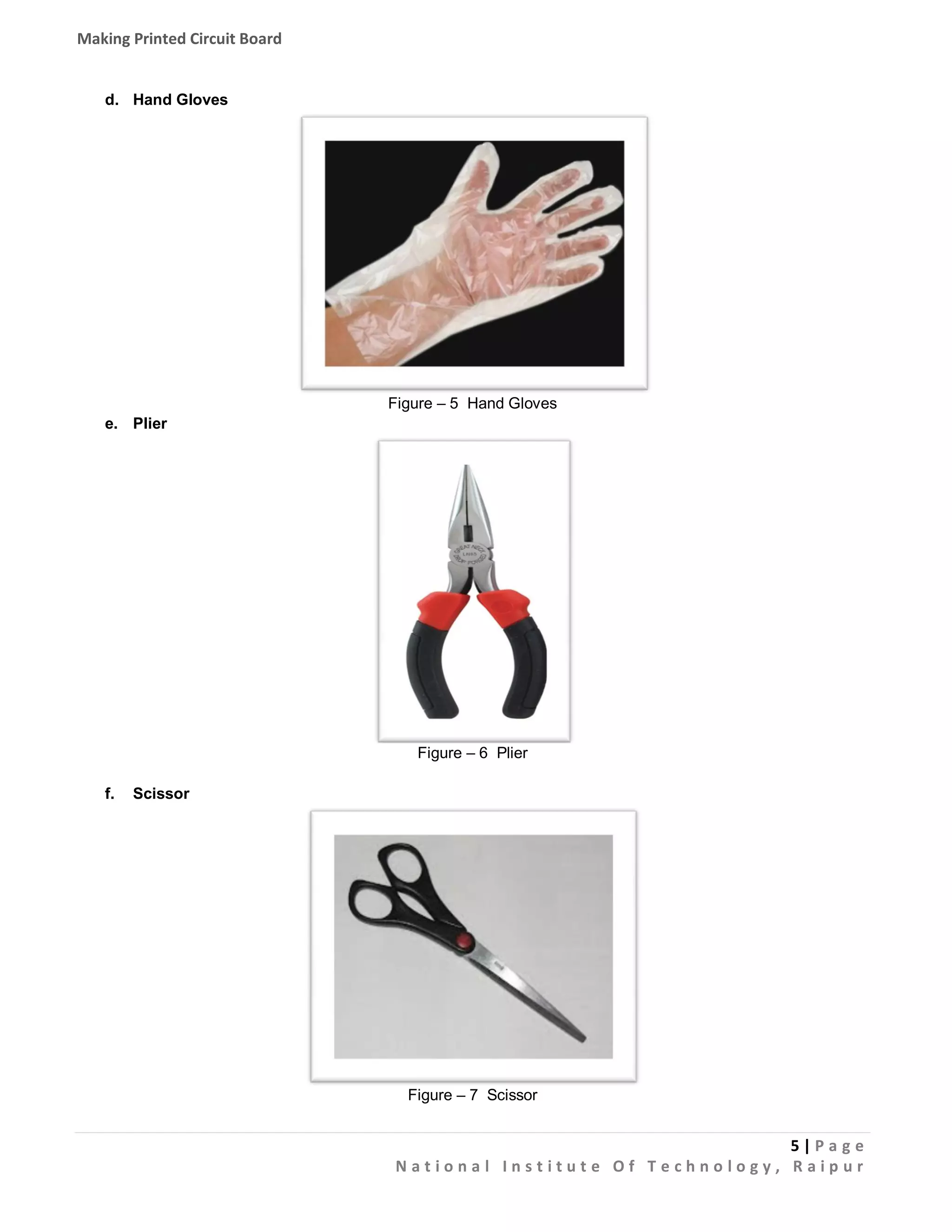
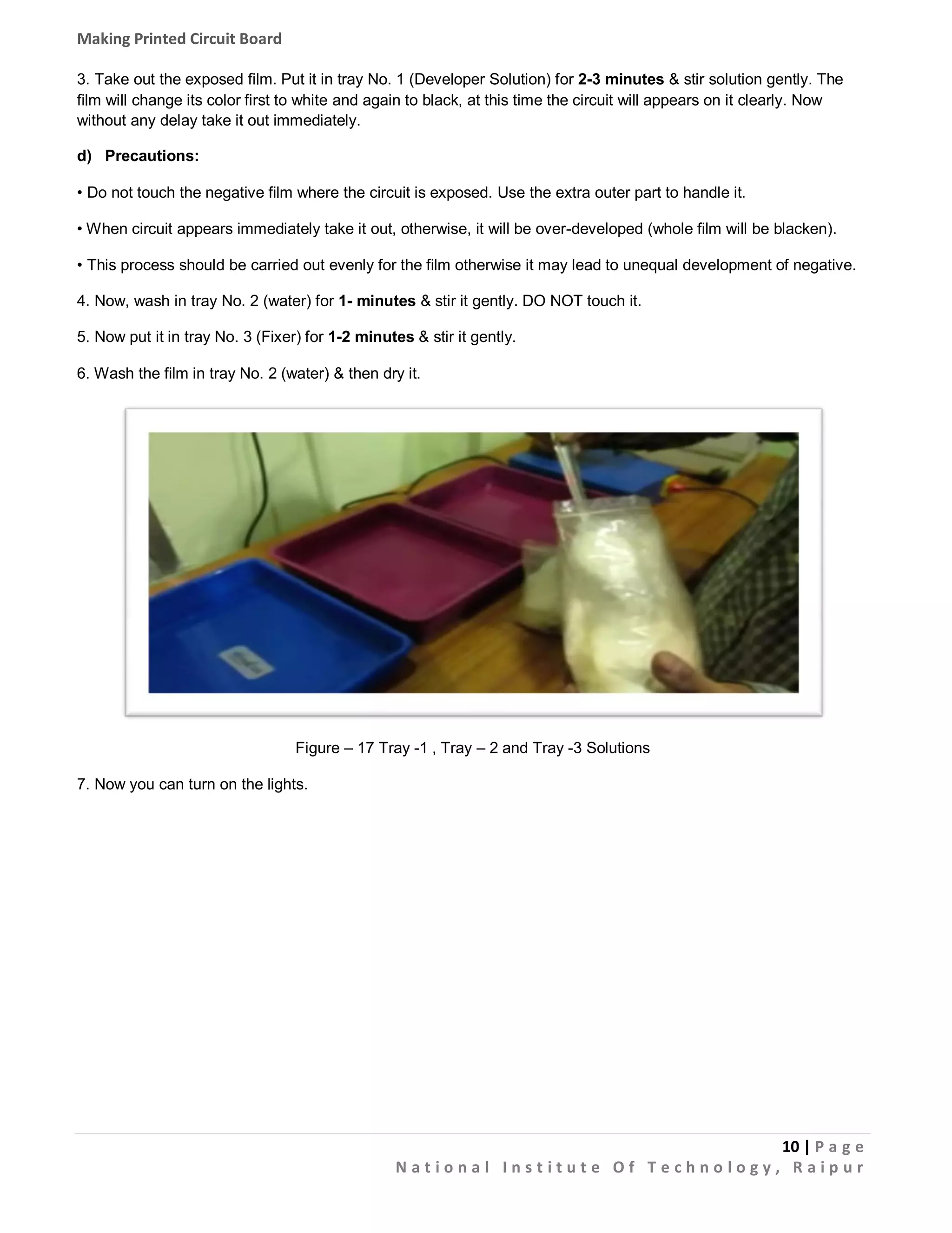
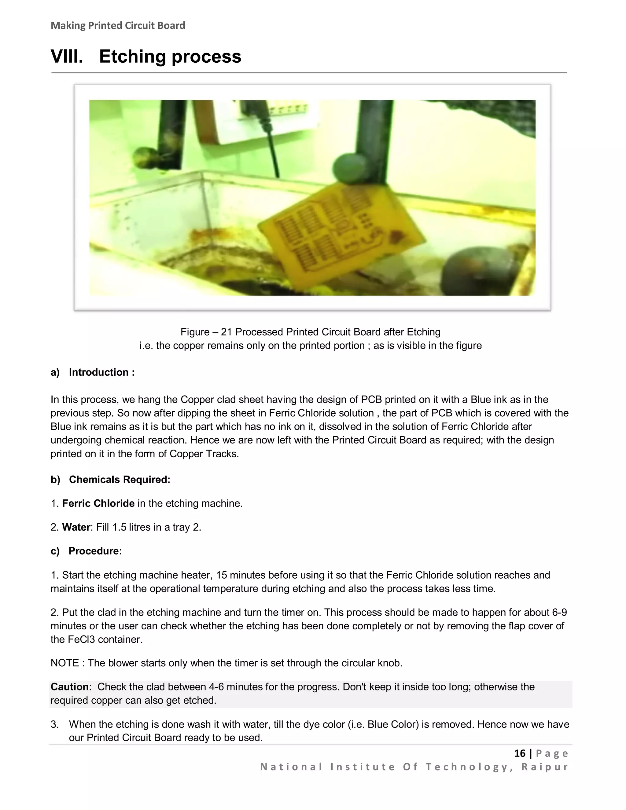
Figure – 16 Dark Room process
[ Taking out the Photo Lith Film from envelope in RED Light ]
b) Chemicals Required:
Chemical A – Sodium Carbonate.
Chemical B - Metol (monomethyl-p-aminophenol hemisulfate), phenidone (1-phenyl-3pyrazolidinone) or dimezone (4,4-dimethyl-1-phenylpphenylpyrazolidin-3-one) etc are
Hydrocarbons.
Negative Developer Solution: Prepare a solution of chemical A (1 spoon) + chemical B (1spoon) & 1.5
litres of water in a tray No. 1.
Water: Fill 1.5 litres in tray No. 2.
Fixer Solution: Prepare a solution of 2 – cap of fixer & 1 litre of water in tray No. 3.
c) Procedure :
1. Take out the negative film from the black envelope. Cut the negative film into the desired size of the layout. It is
to note that negative film has two different sides, one is white & other is black. Black side is used for exposure
purpose.
Caution : Don’t open the black envelope and photo lith film in daylight or normal light. Otherwise, the negative
paper will be exposed and no further process can be carried out with it.
2. Use tape to fix the circuit printed trace paper on the photo lith film, black side of film facing the trace paper.
Now keep this on glass of Proto Contact Film Maker, trace paper facing downward. Close the flap TIGHTLY.
Turn the machine on and expose the film by pressing the push switch for 10-12 seconds.
Caution: Do not turn on the machine before placing the negative paper (photo sensitive film) over on it.
9|Pa g e
National Institute Of Technology, Raipur](https://image.slidesharecdn.com/printedcircuitboard-alaboratoryprocess-140223114232-phpapp02/75/Printed-circuit-board-A-laboratory-process-for-making-PCB-9-2048.jpg)
![Making Printed Circuit Board
V. Copper clad preparation [Photo Resist Dip Coating]
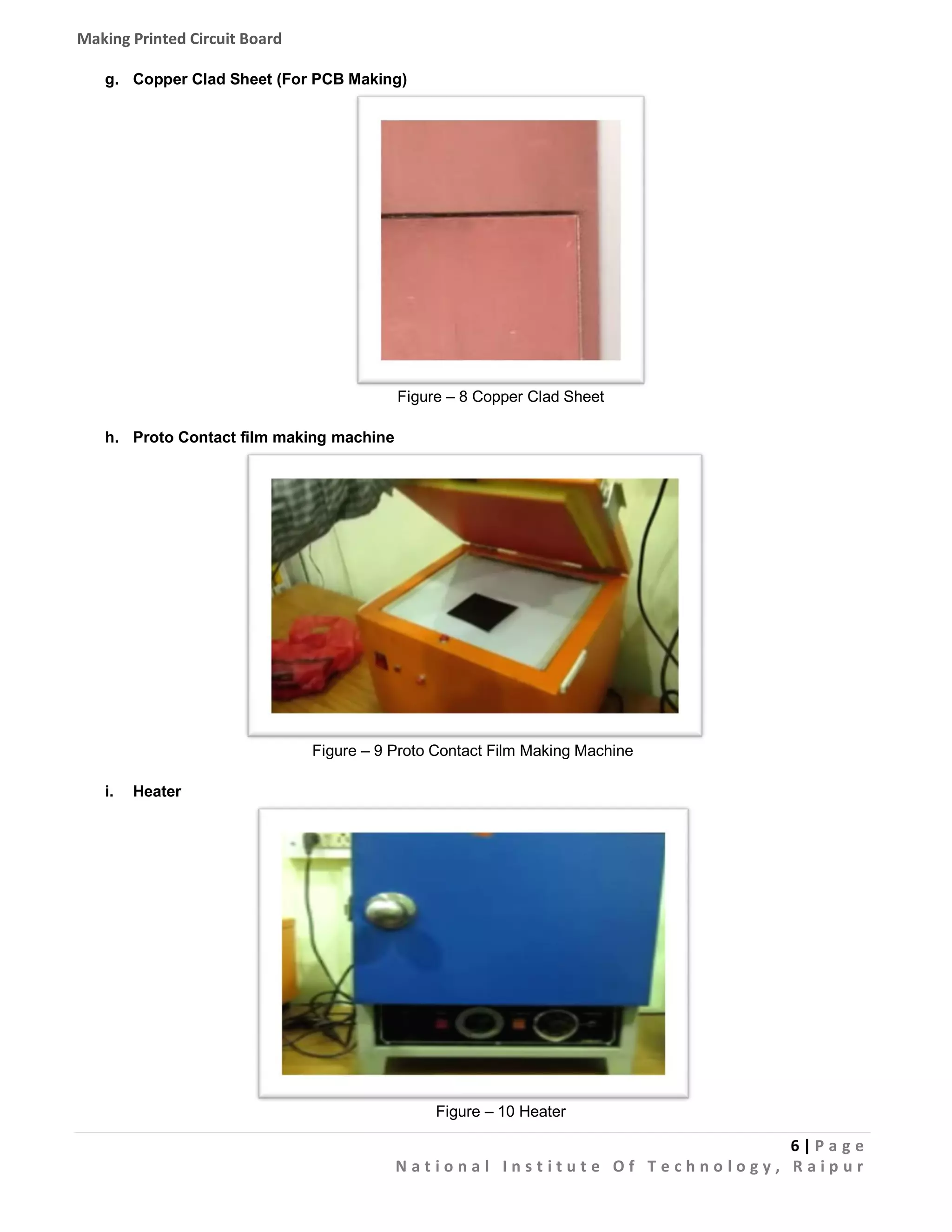
Figure – 18 Copper Clad hanging on the clip ready for the Photo Resist Dip Coating
a) Introduction
Photoresists are classified into two groups: positive resists and negative resists :
1. A Positive resist is a type of photoresist in which the portion of the photoresist that is exposed to light
becomes soluble to the photoresist developer. The portion of the photoresist that is unexposed remains
insoluble to the photoresist developer.
2. A Negative resist is a type of photoresist in which the portion of the photoresist that is exposed to light
becomes insoluble to the photoresist developer. The unexposed portion of the photoresist is dissolved by the
photoresist developer.
b) Chemicals Required:
1. Photo-Resist Solution: Fill the Dip coating machine with Photo Resist Chemical – Poly Methyl Methacrylate
(PMMA) solution. If it is too viscous, dilute it with Thinner.
c) Alternatives for Chemicals Used
Poly(methyl methacrylate) (PMMA).
Poly(methyl glutarimide) (PMGI).
Phenol formaldehyde resin (DNQ/Novolac).
SU-8.
d) Procedure:
1. Take out the Copper Clad & cut it in desired size with the help of Cutter machine (See Figure - 15).
2. Now, Clean the Copper side with metal scrubber and wash it.
3. Turn On the Photo Resist Dip Coating Machine. Put the Copper Clad Sheet on the hook of Photo Resist Dip
Coating Machine. Move lever DOWN & keep it inside the solution for 1 minute. Now, take it out & dry it in air.
11 | P a g e
National Institute Of Technology, Raipur](https://image.slidesharecdn.com/printedcircuitboard-alaboratoryprocess-140223114232-phpapp02/75/Printed-circuit-board-A-laboratory-process-for-making-PCB-11-2048.jpg)
![Making Printed Circuit Board
VI. Ultra Violet exposure & developing
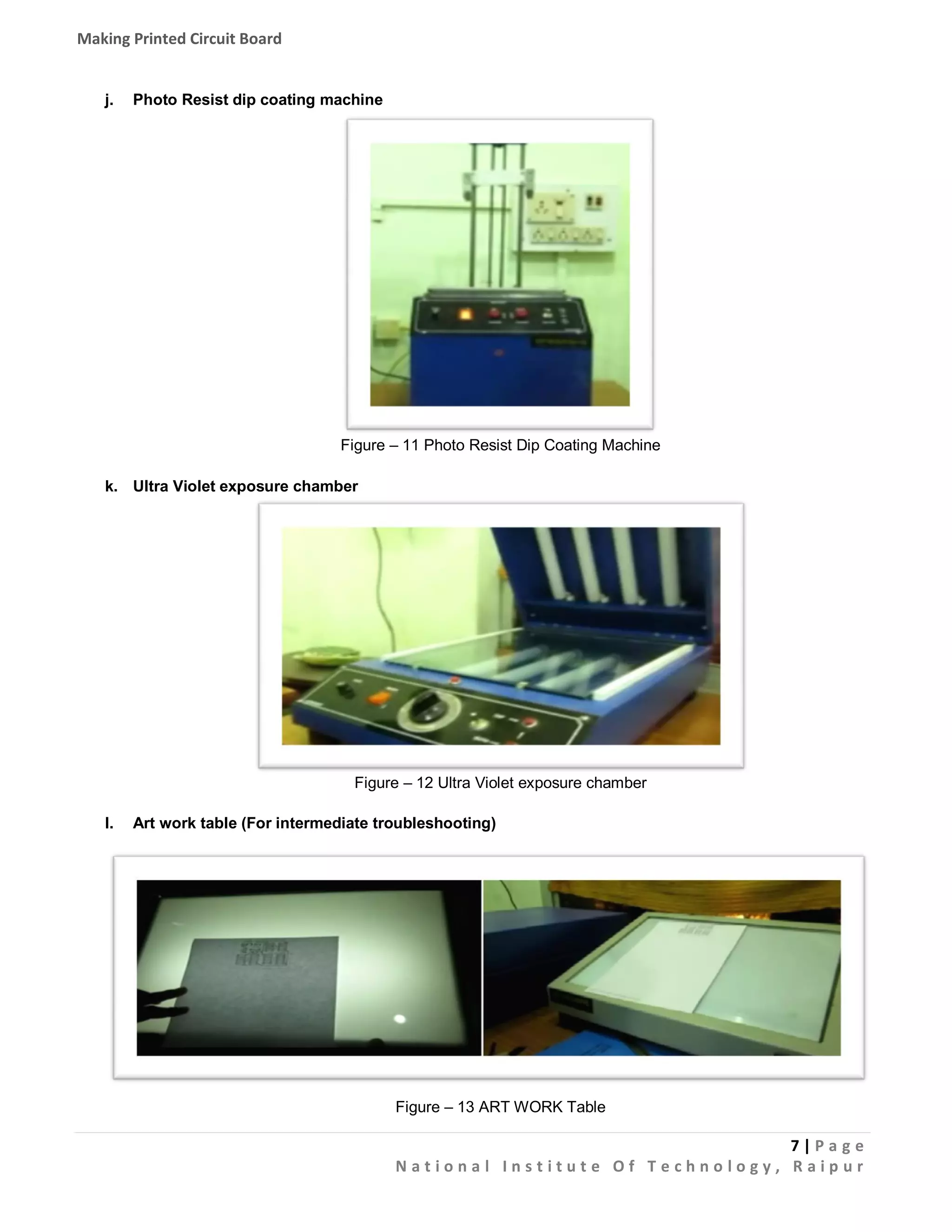
Figure – 19 Film stuck over the photo resist coated copper clad sheet
ready for the Ultra Violet Exposure
a) Introduction :
In this process , the Copper Clad + Film pair is exposed to the Ultra Violet Rays in the UV Chamber , so that after
developing the UV Exposed Copper Clad sheet, the exposed part (Black Tracks / lines of the Circuit in the PCB
design shown in Figure - 2 ) gets rough compared to the other part which was not exposed to ultra violet. This
rough surface as we know is the required part of our Printed circuit board. So in the further process, we apply the
Blue ink/ dye so that the blue ink gets stuck only to the rough part.
b) Chemicals Required:
1. Developer: Fill Developer Solution (Developer (For Copper Clad Developing)) - The UV Exposed Copper Clad
sheet in PCB Making process is developed with a 1% solution of sodium hydroxide [NaOH]. You can make this
solvent by adding 10 gram of sodium hydroxide pellets to 1 litre of water and mix it until everything is dissolved) in
a jar or tray.
2. Water: Fill 1.5 litres in a tray.
3. Blue Dye.
c) Procedure:
1. Fix the negative on the copper side of Copper Clad using tape. (Place the negative correctly facing the clad
otherwise your circuit will be Mirror of what you want to get.)
2. Put it in UV-Exposure machine between the glasses with Copper layer upside. Set the timer for 6 minutes. Use
TOP for single layer PCB and BOTH SIDE for double layer one.
Caution: Watch for any air gap between negative & Copper Clad. It should be tightly pressed between the
glasses.
3. Remove the negative from the copper clad & put it in Copper Clad LPR developer for 2-3 minutes. Stir it gently.
13 | P a g e
National Institute Of Technology, Raipur](https://image.slidesharecdn.com/printedcircuitboard-alaboratoryprocess-140223114232-phpapp02/75/Printed-circuit-board-A-laboratory-process-for-making-PCB-13-2048.jpg)

The document describes the process for making a printed circuit board (PCB) in 8 steps: 1. Designing the circuit layout and creating a negative film of the design. 2. Coating copper clad sheet with photo resist using a dip coating machine. 3. Exposing the photo resist coated sheet and developing it to reveal the circuit pattern. 4. Drilling holes in the board at connection points. 5. Etching away excess copper, leaving the circuit pattern. 6. The process involves chemicals like ferric chloride, sodium hydroxide and photo resist to develop and etch the circuit board. Precise steps and safety procedures are followed to successfully create the PCB.


