Downloaded 32 times

![Page | 19
1. Schematic capture through an Electronic design automation tool.
2. Card dimensions and template are decided based on required circuitry and case of the PCB.
Determine the fixed components and heat sinks if required.
3. Deciding stack layers of the PCB. 1 to 12 layers or more depending on design complexity.
Ground plane and power plane are decided. Signal planes where signals are routed are in top
layer as well as internal layers.[31]
4. Line impedance determination using dielectric layer thickness, routing copper thickness and
trace-width. Trace separation also taken into account in case of differential signals. Microstrip,
stripline or dual stripline can be used to route signals.
5. Placement of the components. Thermal considerations and geometry are taken into account.
Vias and lands are marked.
6.Routing the signal traces. For optimal EMI performance high frequency signals are routed in
internal layers between power or ground planes as power planes behave as ground for AC.
7. Gerber file generation for manufacturing.
In the design of the PCB artwork, a power plane is the counterpart to the ground plane and
behaves as an AC signal ground, while providing DC voltage for powering circuits mounted on
the PCB. In electronic design automation (EDA) design tools, power planes (and ground planes)
are usually drawn automatically as a negative layer, with clearances or connections to the plane
created automatically.
4.1COPPERTHICKNESS
Copper thickness of PCBs can be specified in units of length, but is often specified as weight of
copper per square foot, in ounces, which is easier to measure. Each ounce of copper is
approximately 1.4 mils (0.0014 inch) or 35 μm of thickness.
The printed circuit board industry defines heavy copper as layers exceeding 3 ounces of copper,
or approximately 0.0042 inches (4.2 mils, 105 μm) thick. PCB designers and fabricators often
use heavy copper when design and manufacturing circuit boards in order to increase current-
carrying capacity as well as resistance to thermal strains.
Heavy copper plated vias transfer heat to external heat sinks. IPC 2152 is a standard for
determining current-carrying capacity of printed circuit board traces](https://image.slidesharecdn.com/projectreport-copy-150901073452-lva1-app6891/75/PCB-19-2048.jpg)

![Page | 26
pick-and-place machines remove the parts from the tapes, tubes or trays and place them on the
PCB.
The boards are then conveyed into the reflow soldering oven. They first enter a pre-heat zone,
where the temperature of the board and all the components is gradually, uniformly raised. The
boards then enter a zone where the temperature is high enough to melt the solder particles in the
solder paste, bonding the component leads to the pads on the circuit board. The surface tension
of the molten solder helps keep the components in place, and if the solder pad geometries are
correctly designed, surface tension automatically aligns the components on their pads. There are
a number of techniques for reflowing solder. One is to use infrared lamps; this is called infrared
reflow. Another is to use a hot gas convection. Another technology which is becoming popular
again is special fluorocarbon liquids with high boiling points which use a method called vapor
phase reflow. Due to environmental concerns, this method was falling out of favor until lead-free
legislation was introduced which requires tighter controls on soldering. Currently, at the end of
2008, convection soldering is the most popular reflow technology using either standard air or
nitrogen gas. Each method has its advantages and disadvantages. With infrared reflow, the board
designer must lay the board out so that short components don't fall into the shadows of tall
components. Component location is less restricted if the designer knows that vapor phase reflow
or convection soldering will be used in production. Following reflow soldering, certain irregular
or heat-sensitive components may be installed and soldered by hand, or in large-scale
automation, by focused infrared beam (FIB) or localized convection equipment.
If the circuit board is double-sided then this printing, placement, reflow process may be repeated
using either solder paste or glue to hold the components in place. If a wave soldering process is
used, then the parts must be glued to the board prior to processing to prevent them from floating
off when the solder paste holding them in place is melted.
After soldering, the boards may be washed to remove flux residues and any stray solder balls that
could short out closely spaced component leads. Rosin flux is removed with fluorocarbon
solvents, high flash point hydrocarbon solvents, or low flash solvents e.g. limonene (derived
from orange peels) which require extra rinsing or drying cycles. Water-soluble fluxes are
removed with deionized water and detergent, followed by an air blast to quickly remove residual
water. However, most electronic assemblies are made using a "No-Clean" process where the flux
residues are designed to be left on the circuit board [benign]. This saves the cost of cleaning,
speeds up the manufacturing process, and reduces waste.
Certain manufacturing standards, such as those written by the IPC - Association Connecting
Electronics Industries require cleaning regardless of the solder flux type used to ensure a
thoroughly clean board. Even no-clean flux leaves a residue which, under IPC standards, must be
removed. Proper cleaning removes all traces of solder flux, as well as dirt and other
contaminants that may be invisible to the naked eye. However, while shops conforming to IPC
standard are expected to adhere to the Association's rules on board condition, not all
manufacturing facilities apply IPC standard, nor are they required to do so. Additionally, in some](https://image.slidesharecdn.com/projectreport-copy-150901073452-lva1-app6891/75/PCB-26-2048.jpg)

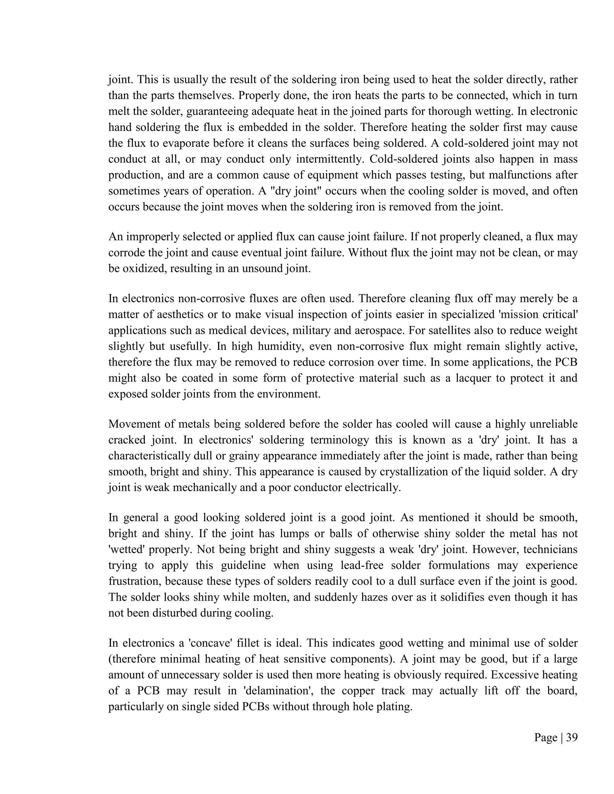

Instrumentation Limited (IL) is an Indian government enterprise established in 1964 to achieve self-reliance in control and automation technology for process industries. IL manufactures and supplies advanced control equipment on a turnkey basis to various industry sectors. It has manufacturing facilities in Kota and Palakkad, India and a network of offices across India to provide installation, commissioning and after-sales services. With over 45 years of experience, IL designs, engineers, manufactures, integrates, installs and commissions complex control systems and has diversified into various related fields to offer a comprehensive range of products and services.