Downloaded 12 times


![FETCHING A WORD FROM MEMORY:
As an example, assume that the address of the memory
location to be accessed is kept in register R2 and that the
memory contents to be loaded into register R1. This is
done by the following sequence of operations:
1. MAR [R2] 2. Read
3. Wait for MFC signal 4. R1 [MDR]
The time required for step 3 depends on the speed of the
memory unit. In general, the time required to access a
word from the memory is longer than the time required
to perform any operation within the CPU.](https://image.slidesharecdn.com/precessororganization-161003071813/85/Precessor-organization-9-320.jpg)
![STORING A WORD INTO MEMORY:
•The procedure of writing a word into memory location is similar to that for reading
one from memory. The only difference is that the data word to be written is first
loaded into the MDR, the write command is issued.
•As an example, assumes that the data word to be stored in the memory is in register
R1 and that the memory address is in register R2. The memory write operation
requires the following sequence:
1. MAR [R2]
2. MDR [R1]
3. Write
4. Wait for MFC
•In this case step 1 and step 2 are independent and so they can be carried out in any
order. In fact, step 1 and 2 can be carried out simultaneously, if this is allowed by the
architecture, that is, if these two data transfers (memory address and data) do not use
the same data path.
•In case of both memory read and memory write operation, the total time duration
depends on wait for the MFC signal, which depends on the speed of the memory
module.](https://image.slidesharecdn.com/precessororganization-161003071813/85/Precessor-organization-10-320.jpg)


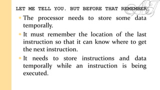
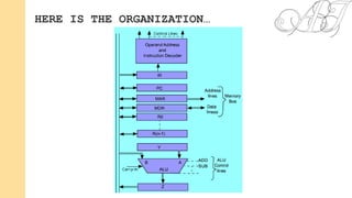
- The processor stores data and instructions temporarily in registers during execution. It needs registers to store the location of the current instruction and data/instructions being used. - An instruction cycle involves fetching the next instruction from memory, decoding it, and executing it. Fetching involves reading the instruction from memory into the processor. Execution interprets the instruction and performs the specified operation. - Common operations include fetching data from memory into a register, storing a register to memory, transferring between registers, and arithmetic/logic operations using the ALU with results stored in a register. Fetching and storing involve transferring addresses and data between the memory address register (MAR), memory data register (MDR), and memory bus.