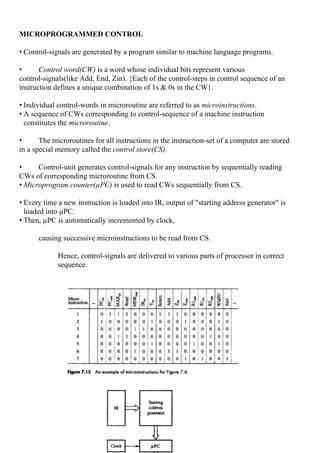
The document discusses the basic components and processes of a basic processing unit. It contains 3 key points:
1) To execute an instruction, a processor must fetch the instruction from memory, increment the program counter, and carry out the actions specified by the instruction. The first two steps are the fetch phase and the third step is the execution phase.
2) Registers, memory, and an arithmetic logic unit (ALU) are the main components. Instructions are executed by transferring data between registers and performing arithmetic or logic operations in the ALU.
3) Branching instructions allow the program counter to be loaded with a new address, allowing different execution paths. Conditional branches check status flags before branching.
![BASIC PROCESSING UNIT
SOME FUNDAMENTAL CONCEPTS
• To execute an instruction, processor has to perform following 3 steps:
1) Fetch contents of memory-location pointed to by PC. Content of this location
is an instruction to be executed. The instructions are loaded into IR, Symbolically,
this operation can be written as
IR->[[PC]]
2)Increment PC by 4
3)Carry out the actions specified by instruction (in the IR).
• The first 2 steps are referred to as fetch phase;
Step 3 is referred to as execution phase.
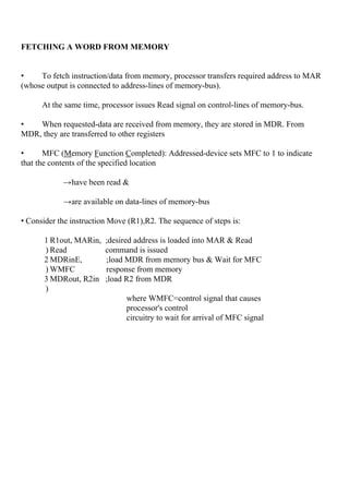
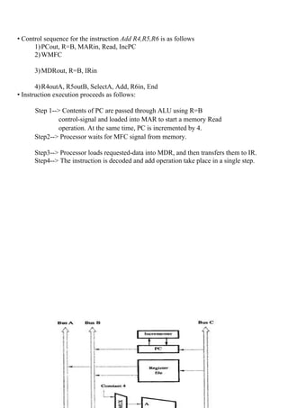
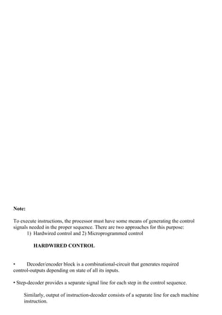
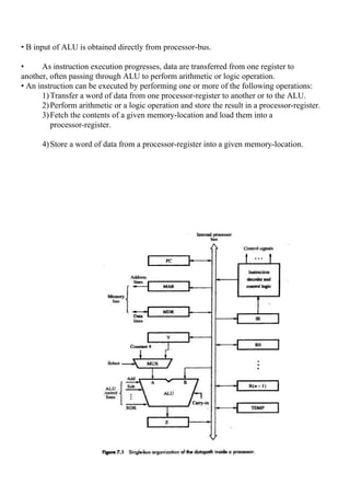
SINGLE BUS ORGANIZATION
• MDR has 2 inputs and 2 outputs. Data may be loaded
→into MDR either from memory-bus (external) or
→from processor-bus (internal).
• MAR‟s input is connected to internal-bus, and
• Instruction-decoder & control-unit is responsible for
→ issuing the signals that control the operation of all the units inside
the processor (and for interacting with memory bus).
→implementing the actions specified by the instruction (loaded in the IR)
• Registers R0 through R(n-1) are provided for general purpose use by programmer.
• Three registers Y, Z & TEMP are used by processor for temporary storage during
execution of some instructions. These are transparent to the programmer i.e. programmer
need not be concerned with them because they are never referenced explicitly by any
instruction.
• MUX(Multiplexer) selects either
→output of Y or
→constant-value 4(is used to increment PC content). This is provided as input A of
ALU.](https://image.slidesharecdn.com/co-7thunit-191117044920/85/Computer-Organization-1-320.jpg)
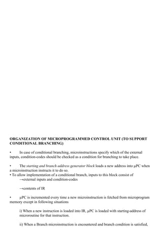
![BASIC PROCESSING UNIT
SOME FUNDAMENTAL CONCEPTS
• To execute an instruction, processor has to perform following 3 steps:
1) Fetch contents of memory-location pointed to by PC. Content of this location
is an instruction to be executed. The instructions are loaded into IR, Symbolically,
this operation can be written as
IR->[[PC]]
2)Increment PC by 4
3)Carry out the actions specified by instruction (in the IR).
• The first 2 steps are referred to as fetch phase;
Step 3 is referred to as execution phase.
SINGLE BUS ORGANIZATION
• MDR has 2 inputs and 2 outputs. Data may be loaded
→into MDR either from memory-bus (external) or
→from processor-bus (internal).
• MAR‟s input is connected to internal-bus, and
• Instruction-decoder & control-unit is responsible for
→ issuing the signals that control the operation of all the units inside
the processor (and for interacting with memory bus).
→implementing the actions specified by the instruction (loaded in the IR)
• Registers R0 through R(n-1) are provided for general purpose use by programmer.
• Three registers Y, Z & TEMP are used by processor for temporary storage during
execution of some instructions. These are transparent to the programmer i.e. programmer
need not be concerned with them because they are never referenced explicitly by any
instruction.
• MUX(Multiplexer) selects either
→output of Y or
→constant-value 4(is used to increment PC content). This is provided as input A of
ALU.](https://image.slidesharecdn.com/co-7thunit-191117044920/75/Computer-Organization-1-2048.jpg)
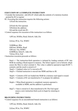
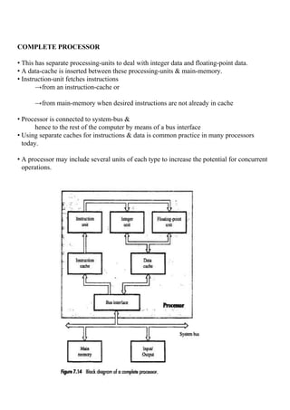
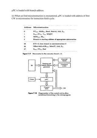
![PERFORMING AN ARITHMETIC OR LOGIC OPERATION
• The ALU performs arithmetic operations on the 2 operands applied to its A and B inputs.
• One of the operands is output of MUX &
the other operand is obtained directly from bus.
• The result (produced by the ALU) is stored temporarily in register Z.
• The sequence of operations for [R3][R1]+[R2] is as follows
1) R1out, Yin //transfer the contents of R1 to Y register
2)R2out, SelectY, Add, Zin//R2 contents are transferred directly to B input of ALU.
// The numbers of added. Sum stored in register Z
3) Zout, R3in //sum is transferred to register R3
• The signals are activated for the duration of the clock cycle corresponding to that
step. All other signals are inactive.
•
Write the complete control sequence for the instruction : Move (Rs),Rd
• This instruction copies the contents of memory-location pointed to by Rs into Rd.
This is a memory read operation. This requires the following actions
→fetch the instruction
→fetch the operand (i.e. the contents of the memory-location pointed by Rs).
→transfer the data to Rd.
• The control-sequence is written as follows
1)PCout, MARin, Read, Select4, Add, Zin
2)Zout, PCin, Yin, WMFC
3)MDRout, IRin
4)Rs, MARin, Read
5)MDRinE, WMFC
6)MDRout, Rd, End](https://image.slidesharecdn.com/co-7thunit-191117044920/85/Computer-Organization-5-320.jpg)