Contents
Introduction
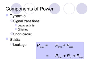
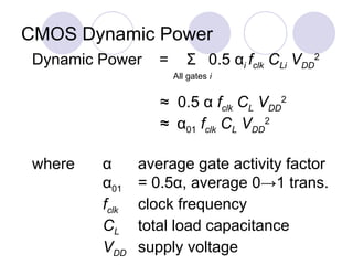
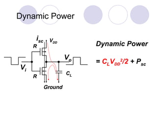
Dynamic power
Short circuitpower
Reduced supply voltage operation
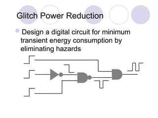
Glitch elimination
Static (leakage) power reduction
Low power systems
State encoding
Processor and multi-core design
Books on low-power design
3.
Introduction
Why is ita concern?
Business & technical needs
Semiconductor processing technology
Power Consumption of VLSI Chips
4.
NEED FOR LOWPOWER
More transistors are packed into the chip.
Increased market demand for portable
devices.
Environmental concerns
5.
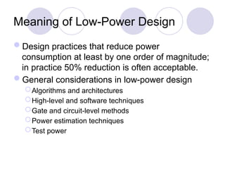
Meaning of Low-PowerDesign
Design practices that reduce power
consumption at least by one order of magnitude;
in practice 50% reduction is often acceptable.
General considerations in low-power design
Algorithms and architectures
High-level and software techniques
Gate and circuit-level methods
Power estimation techniques
Test power
6.
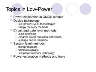
Topics in Low-Power
Powerdissipation in CMOS circuits
Device technology
Low-power CMOS technologies
Energy recovery methods
Circuit and gate level methods
Logic synthesis
Dynamic power reduction techniques
Leakage power reduction
System level methods
Microprocessors
Arithmetic circuits
Low power memory technology
Power estimation methods and tools
7.
Low-Power Design Techniques
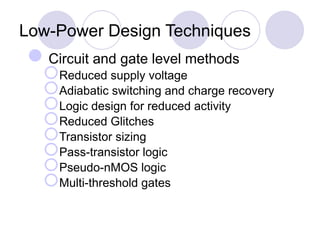
Circuitand gate level methods
Reduced supply voltage
Adiabatic switching and charge recovery
Logic design for reduced activity
Reduced Glitches
Transistor sizing
Pass-transistor logic
Pseudo-nMOS logic
Multi-threshold gates
8.
Low-Power Design Techniques
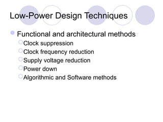
Functionaland architectural methods
Clock suppression
Clock frequency reduction
Supply voltage reduction
Power down
Algorithmic and Software methods
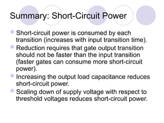
Summary: Short-Circuit Power
Short-circuitpower is consumed by each
transition (increases with input transition time).
Reduction requires that gate output transition
should not be faster than the input transition
(faster gates can consume more short-circuit
power).
Increasing the output load capacitance reduces
short-circuit power.
Scaling down of supply voltage with respect to
threshold voltages reduces short-circuit power.
15.
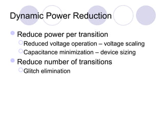
Dynamic Power Reduction
Reducepower per transition
Reduced voltage operation – voltage scaling
Capacitance minimization – device sizing
Reduce number of transitions
Glitch elimination
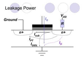
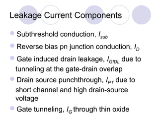
Leakage Current Components
Subthresholdconduction, Isub
Reverse bias pn junction conduction, ID
Gate induced drain leakage, IGIDL due to
tunneling at the gate-drain overlap
Drain source punchthrough, IPT due to
short channel and high drain-source
voltage
Gate tunneling, IG through thin oxide
20.
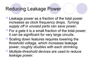
Reducing Leakage Power
Leakagepower as a fraction of the total power
increases as clock frequency drops. Turning
supply off in unused parts can save power.
For a gate it is a small fraction of the total power;
it can be significant for very large circuits.
Scaling down features requires lowering the
threshold voltage, which increases leakage
power; roughly doubles with each shrinking.
Multiple-threshold devices are used to reduce
leakage power.
21.
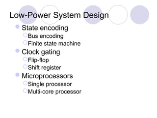
Low-Power System Design
Stateencoding
Bus encoding
Finite state machine
Clock gating
Flip-flop
Shift register
Microprocessors
Single processor
Multi-core processor
22.
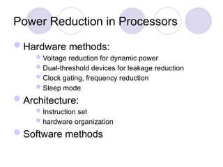
Power Reduction inProcessors
Hardware methods:
Voltage reduction for dynamic power
Dual-threshold devices for leakage reduction
Clock gating, frequency reduction
Sleep mode
Architecture:
Instruction set
hardware organization
Software methods
23.
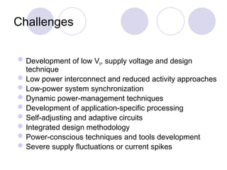
Challenges
Development of lowVt, supply voltage and design
technique
Low power interconnect and reduced activity approaches
Low-power system synchronization
Dynamic power-management techniques
Development of application-specific processing
Self-adjusting and adaptive circuits
Integrated design methodology
Power-conscious techniques and tools development
Severe supply fluctuations or current spikes