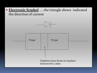
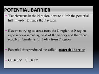
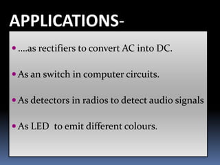
P-N JUNCTION
DIODE
P-N JUNCTION :-A p–n junction is a
boundary or interface between two
types of semiconductor material, p-
type and n-type, inside a single crystal
of semiconductor. It is created by
doping.
 Electronic Symbol …..the triangle shows indicated
the direction of current
Depletion layer forms an insulator
between the 2 sides
P type N type
Formation of depletion layer
the excess electrons in the N region cross the junction
and combine with the excess holes in the P region.
N region loses its electrons ……becomes + vlY charged
P region accepts the electrons ……becomes –vly charged
At one point , the migratory action is stopped.
 An additional electrons from the N region are repelled
by the net negative charge of the p region.
Similarly,
 An additional holes from the P region are repelled by
the net positive charge of the n region.
 Net result
a creation of a thin layer of each side of the junction
……….which is depleted (emptied) of mobile charge
carriers…. This is known as DEPLETION LAYER
..Thickness is of the order of 10-6meter.
The depletion layer contains no free and
mobile charge carriers but only fixed and
immobile ions.
Its width depends upon the doping level..
Heavy doped……..thin depletion layer
lightly doped……..thick depletion layer
POTENTIAL BARRIER
 The electrons in the N region have to climb the potential
hill in order to reach the P region
 Electrons trying to cross from the N region to P region
experience a retarding field of the battery and therefore
repelled. Similarly for holes from P region.
 Potential thus produced are called ..potential barrier
 Ge..0.3 V Si ..0.7V
PN junction can basically work in two modes, (A
battery is connected to the diode )
forward bias mode ( positive terminal
connected to p-region and negative terminal
connected to n region)
reverse bias mode ( negative terminal
connected to p-region and positive terminal
connected to n region) .
Forward biased PN junction
. It forces the majority charge carriers
to move across the junction
….decreasing the width of the
depletion layer.
 Once the junction is crossed, a number of electrons
and the holes will recombine .
 For each hole in the P section that combines with an
electron from the N section, a covalent bond breaks
and an electron is liberatyed which enters the positive
terminal
 Thus creating an electron hole pair.
 Current in the N region is carried by ….electrons
 Current in the P region is carried by …. Holes.
Reverse biased pn junction
 If the + of the battery is connected to the n-type and the
– terminal to the p-type,
the free electrons and free holes are
attracted back towards the battery, hence
back from the depletion layer, hence the
depletion layer grows.
Thus a reverse biased pn junction does not conduct
current.
Thus the P N junction diode allows
the electrons flow only when P is
positive .
This property is used for the
conversion of AC into DC ,Which
is called rectification.
ADVANTAGES:
No filament is necessary
Occupies lesser space
Long life.
APPLICATIONS-
….as rectifiers to convert AC into DC.
As an switch in computer circuits.
As detectors in radios to detect audio signals
As LED to emit different colours.
Thank you

Diode and Rectifier.ppt

  • 1.
  • 2.
    P-N JUNCTION :-Ap–n junction is a boundary or interface between two types of semiconductor material, p- type and n-type, inside a single crystal of semiconductor. It is created by doping.
  • 3.
     Electronic Symbol…..the triangle shows indicated the direction of current Depletion layer forms an insulator between the 2 sides P type N type
  • 4.
    Formation of depletionlayer the excess electrons in the N region cross the junction and combine with the excess holes in the P region. N region loses its electrons ……becomes + vlY charged P region accepts the electrons ……becomes –vly charged At one point , the migratory action is stopped.
  • 5.
     An additionalelectrons from the N region are repelled by the net negative charge of the p region. Similarly,  An additional holes from the P region are repelled by the net positive charge of the n region.  Net result a creation of a thin layer of each side of the junction ……….which is depleted (emptied) of mobile charge carriers…. This is known as DEPLETION LAYER ..Thickness is of the order of 10-6meter.
  • 6.
    The depletion layercontains no free and mobile charge carriers but only fixed and immobile ions. Its width depends upon the doping level.. Heavy doped……..thin depletion layer lightly doped……..thick depletion layer
  • 7.
    POTENTIAL BARRIER  Theelectrons in the N region have to climb the potential hill in order to reach the P region  Electrons trying to cross from the N region to P region experience a retarding field of the battery and therefore repelled. Similarly for holes from P region.  Potential thus produced are called ..potential barrier  Ge..0.3 V Si ..0.7V
  • 8.
    PN junction canbasically work in two modes, (A battery is connected to the diode ) forward bias mode ( positive terminal connected to p-region and negative terminal connected to n region) reverse bias mode ( negative terminal connected to p-region and positive terminal connected to n region) .
  • 9.
    Forward biased PNjunction . It forces the majority charge carriers to move across the junction ….decreasing the width of the depletion layer.
  • 10.
     Once thejunction is crossed, a number of electrons and the holes will recombine .  For each hole in the P section that combines with an electron from the N section, a covalent bond breaks and an electron is liberatyed which enters the positive terminal  Thus creating an electron hole pair.  Current in the N region is carried by ….electrons  Current in the P region is carried by …. Holes.
  • 11.
    Reverse biased pnjunction  If the + of the battery is connected to the n-type and the – terminal to the p-type, the free electrons and free holes are attracted back towards the battery, hence back from the depletion layer, hence the depletion layer grows. Thus a reverse biased pn junction does not conduct current.
  • 12.
    Thus the PN junction diode allows the electrons flow only when P is positive . This property is used for the conversion of AC into DC ,Which is called rectification.
  • 14.
    ADVANTAGES: No filament isnecessary Occupies lesser space Long life.
  • 15.
    APPLICATIONS- ….as rectifiers toconvert AC into DC. As an switch in computer circuits. As detectors in radios to detect audio signals As LED to emit different colours.
  • 31.