Lecture 1


 Introduction

Dr. Mashiur Rahman
The history
• The Vision: In 1959, Caltech physicist Richard Feynman
  gives his famed talk ―There‘s Plenty of Room at the
  Bottom,‖ outlining the prospects for atomic engineering.
• Seeing is Believing: In 1981, Gerd Binnig and Heinrich
  Rohrer of IBM‘s Zurich Research Laboratory create the
  scanning tunneling microscope, enabling researchers to
  both see and manipulate atoms for the first time.
• Nanostructures: In 1985, Robert F. Curl Jr., Harold W.
  Kroto, and Richard E. Smalley discover
  buckminsterfullerenes (buckyballs — refer to Figure 1-1),
  soccer-ball-shaped molecules made of carbon and
  measuring roughly 0.7nm wide.
There‘s Plenty of Room at the Bottom
                ―People tell me about miniaturization, and how far it
                has progressed today. They tell me about electric
                motors that are the size of the nail on your small
                finger. And there is a device on the market, they tell
                me, by which you can write the Lord's Prayer on
                the head of a pin.But that's nothing; that's the most
                primitive, halting step in the direction I intend to
                discuss. It is a staggeringly small world that is
Richard Feynman below. In the year 2000, when they look back at
Cal Tech, 1959
                this age, they will wonder why it was not until the
                year 1960 that anybody began seriously to move in
                this direction. Why cannot we write the entire 24
                volumes of the Encyclopedia Brittanica on the head
                of a pin?‖
This goal requires patterning at the 10 nanometer scale.
Invention of the Transistor
The first planar integrated circuit, 1961
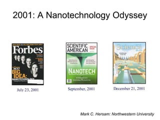
2001: A Nanotechnology Odyssey


               Mark C. Hersam: Northwestern University
Red Herring, May 2002
Funding in
nanotechnology industry
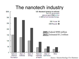
The nanotech industry


            2005: Federal $980 million
            2015: Estimated $1.2 trillion


                    Source: Nanotechnology For Dummies
Total number of patent applications in nanotechnology between
1995 and 2003, and (inset) the proportion of applications in 2003 in
six subfields defined by the European Patent Office. b, Number of
patent applications from the Americas, Asia and Europe.
The world according to nano
Market Analysis - Major Results
Source: Business Communication Co. Inc.


Nanopnrticde world market by application area. Total 2000 market was S492.5
million. Total 2005 market expected to be $900.1 milliort. (a) energy, curtalytic and
stntctitml applicwtiotts; (b) biomedical, phannacerttical and cosmetic applications;
and (c) elecwonic, magnetic and optoelectronic applications).
A FEW TARGETS FOR
    NANOSCIENCE/TECHNOLOGY
•   ADVANCED MATERIALS
•   FIVE-MINUTE HEALTH SWAB TEST
•   INTERACTIVE GLUCOSE SENSING, DOSING
•   HUMAN REPAIR
•   OPTICAL COMPUTERS
•   GREASELESS SUNTAN LOTION
•   NONFREEZING WINDSHIELDS
•   STAINLESS TIES FOR SOUP SPILLERS
•   SELF-MONITORING FOOD PACKAGING
•   NEURONAL INTERFACES
•   FULLY TARGETED DRUG DELIVERY
•   HEATLESS LIGHT
•   TRULY EFFICIENT SOLAR RADIATION CAPTURE
True or False?
                      We should close this office.. Everything that
                      needs to be invented, is already..
                         Director, US Patent Office, 1929

A few computers should be enough
for the society!
Watson (IBM Watson Center fame)


                           640k should be enough for everyone!
                           Bill Gates, 1982


Infectious diseases is now history..
Surgeon General, 1959
Technology Outlook
Introduction to Nano-scale systems
Bangladesh   Dhaka
Dhaka city   National Parliament
Lake   Tree top
Oak branch and leaves   Oak leaf (actual size)
Oak leaf (actual size)   Leaf surface, 10x enlarged
Leaf surface, 100x enlarged   Many cells
                                 HUMAN HAIR
Individual cells   Cell nucleus
Chromatin structure   DNA double strands
Individual molecules and atoms
The Interesting Length Scale
size-dependent behaviors
Size-Dependent Properties
• At the nanometer scale, properties become size-
  dependent. For example,

(1) Thermal properties – melting temperature
(2) Mechanical properties – adhesion, capillary forces
(3) Optical properties – absorption and scattering of light
(4) Electrical properties – tunneling current
(5) Magnetic properties – superparamagnetic effect

New properties enable new applications
At the nanoscale …


Properties can become
SIZE-DEPENDENT


  EXAMPLES –
  STAINED GLASS
  MELTING POINTS OF METAL NANODOTS
Melting Temperature


e.g., 3 nm CdSe nanocrystal melts at 700 K
compared to bulk CdSe at 1678 K
Mechanical Properties
• At the nanoscale, surface and interface forces
  become dominant. For example,

(1) Adhesion forces
(2) Capillary forces
(3) Strain forces

Surface coatings are extremely important to
  prevent sticking in nanoscale electro-mechanical
  systems (NEMS)
Optical Absorption
Modern Use of Nanoparticles: Biosensors
Electrical Properties:
           Tunneling Current
• At the nanometer scale, electrical insulators
  begin to fail to block current flow.
• Quantum mechanical effect known as tunneling.
• Tunneling current increases exponentially as the
  thickness of the insulator is decreased.
• Tunneling is the basis of the scanning tunneling
  microscope and covalent chemical bonding.
Why Nano
• The discovery of novel materials, processes,
  and phenomena at the nanoscale, as well as the
  development of new experimental and
  theoretical techniques for research provide fresh
  opportunities for the development of innovative
  nanosystems and nanostructured materials.
  Nanosystems are expected to find various
  unique applications. Nanostructured materials
  can be made with unique nanostructures and
  properties. This field is expected to open new
  venues in science and technology
Definitions of ICs
•   A chip or an integrated circuit (IC) is a small electronic device made out of a
    semiconductor material. The integrated circuit consists of elements
    inseparably associated and formed on or within a single SUBSTRATE
    (mounting surface). In other words, the circuit components and all
    interconnections are formed as a unit. The first integrated circuit was
    developed in the 1950s by Jack Kilby of Texas Instruments and Robert
    Noyce of Fairchild Semiconductor. Integrated circuits are used for a variety
    of devices, including microprocessors, audio and video equipment, and
    automobiles. Integrated circuits are often classified by the number of
    transistors and other electronic components they contain:
*   SSI (small-scale integration): Up to 100 electronic components per chip
*   MSI (medium-scale integration): From 100 to 3,000 electronic
    components per chip
*   LSI (large-scale integration): From 3,000 to 100,000 electronic
    components per chip
*   VLSI (very large-scale integration): From 100,000 to 1,000,000 electronic
    components per chip
*   ULSI (ultra large-scale integration): More than 1 million electronic
    components per chip
Definition of MEMS

•   Micro electromechanical systems
    (MEMS), or micromachining (also micro-
    manufacturing and microfabrication), in
    the narrow sense, comprises the use of a
    set of manufacturing tools based on batch
    thin and thick film fabrication techniques
    commonly used in the integrated circuit
    industry or IC industry. This involved
    originally mainly Si based mechanical
    devices.
Why miniaturization?
•   Minimizing energy and materials use in       •   Cost/performance advantages
    manufacturing                                •   Improved reproducibility (batch
•   Redundancy and arrays                            concept)
•   Integration with electronics, simplifying    •   Improved accuracy and reliability
    systems (e.g., single point vs. multipoint   •   Minimal invasive ( e.g. mosquito
    measurement)                                     project)
•   Reduction of power budget                    •   Do we have a choice? (see next
•   Faster devices                                   viewgraph- - the Law of Accelerating
                                                     Returns)
•   Increased selectivity and sensitivity
•   Wider dynamic range
•   Exploitation of new effects through the
    breakdown of continuum theory in the
    microdomain


                                                     probiscus is about 75 µm 
Why miniaturization?
•   Evolution (sophistication) of life-forms or
    technology speeds up because they are build
    on their own recorded degree of order. Ray
    Kurzweil calls this The Law of Accelerating
    Returns*
•   This Law of Accelerating Returns gave us ever
    greater order in technology which led to
    computation -- the essence of order.
•   For life-forms DNA provides the record. In the
    case of technology it is the ever improving
    methods to record information.
•   Moore‘s law ** (based on a temporary
    methodology i.e., lithography) is only an
    example of the Law of Accelerating Returns.
    Beyond lithography we may expect further
    progress in miniaturization based on DNA,
    quantum devices, AFM lithography, nanotubes,
    etc.

*Ray Kurzweil in The Age of Spiritual
 Machines
** See next viewgraph
Why miniaturization?
• Moore‘s ‗Law‘: The observation that the logic density
  of silicon integrated circuits (ICs) has followed a curve
  (bits per square inch/transistors) = 2(t - 1962) where t is
  the year. The amounts of information storable on a
  given amount of silicon roughly doubled every year
  since the technology was invented. This relation, first
  mentioned in 1964 by semiconductor engineer
  Gordon Moore (who co-founded Intel four years later)
  held until the late 1970s, at which point the doubling
  period slowed to 18 months. The doubling period
  remained at that value up to late 1999. Moore's Law
  is apparently self-fulfilling.
Summery

ETE444-lec1-nano-introduction.pdf

  • 1.
  • 2.
    The history • TheVision: In 1959, Caltech physicist Richard Feynman gives his famed talk ―There‘s Plenty of Room at the Bottom,‖ outlining the prospects for atomic engineering. • Seeing is Believing: In 1981, Gerd Binnig and Heinrich Rohrer of IBM‘s Zurich Research Laboratory create the scanning tunneling microscope, enabling researchers to both see and manipulate atoms for the first time. • Nanostructures: In 1985, Robert F. Curl Jr., Harold W. Kroto, and Richard E. Smalley discover buckminsterfullerenes (buckyballs — refer to Figure 1-1), soccer-ball-shaped molecules made of carbon and measuring roughly 0.7nm wide.
  • 3.
    There‘s Plenty ofRoom at the Bottom ―People tell me about miniaturization, and how far it has progressed today. They tell me about electric motors that are the size of the nail on your small finger. And there is a device on the market, they tell me, by which you can write the Lord's Prayer on the head of a pin.But that's nothing; that's the most primitive, halting step in the direction I intend to discuss. It is a staggeringly small world that is Richard Feynman below. In the year 2000, when they look back at Cal Tech, 1959 this age, they will wonder why it was not until the year 1960 that anybody began seriously to move in this direction. Why cannot we write the entire 24 volumes of the Encyclopedia Brittanica on the head of a pin?‖ This goal requires patterning at the 10 nanometer scale.
  • 4.
    Invention of theTransistor
  • 5.
    The first planarintegrated circuit, 1961
  • 6.
    2001: A NanotechnologyOdyssey Mark C. Hersam: Northwestern University
  • 7.
  • 8.
  • 9.
    The nanotech industry 2005: Federal $980 million 2015: Estimated $1.2 trillion Source: Nanotechnology For Dummies
  • 11.
    Total number ofpatent applications in nanotechnology between 1995 and 2003, and (inset) the proportion of applications in 2003 in six subfields defined by the European Patent Office. b, Number of patent applications from the Americas, Asia and Europe.
  • 12.
  • 13.
    Market Analysis -Major Results Source: Business Communication Co. Inc. Nanopnrticde world market by application area. Total 2000 market was S492.5 million. Total 2005 market expected to be $900.1 milliort. (a) energy, curtalytic and stntctitml applicwtiotts; (b) biomedical, phannacerttical and cosmetic applications; and (c) elecwonic, magnetic and optoelectronic applications).
  • 14.
    A FEW TARGETSFOR NANOSCIENCE/TECHNOLOGY • ADVANCED MATERIALS • FIVE-MINUTE HEALTH SWAB TEST • INTERACTIVE GLUCOSE SENSING, DOSING • HUMAN REPAIR • OPTICAL COMPUTERS • GREASELESS SUNTAN LOTION • NONFREEZING WINDSHIELDS • STAINLESS TIES FOR SOUP SPILLERS • SELF-MONITORING FOOD PACKAGING • NEURONAL INTERFACES • FULLY TARGETED DRUG DELIVERY • HEATLESS LIGHT • TRULY EFFICIENT SOLAR RADIATION CAPTURE
  • 15.
    True or False? We should close this office.. Everything that needs to be invented, is already.. Director, US Patent Office, 1929 A few computers should be enough for the society! Watson (IBM Watson Center fame) 640k should be enough for everyone! Bill Gates, 1982 Infectious diseases is now history.. Surgeon General, 1959
  • 16.
  • 17.
  • 18.
  • 19.
    Dhaka city National Parliament
  • 20.
    Lake Tree top
  • 21.
    Oak branch andleaves Oak leaf (actual size)
  • 22.
    Oak leaf (actualsize) Leaf surface, 10x enlarged
  • 23.
    Leaf surface, 100xenlarged Many cells HUMAN HAIR
  • 24.
    Individual cells Cell nucleus
  • 25.
    Chromatin structure DNA double strands
  • 26.
  • 27.
  • 28.
  • 29.
    Size-Dependent Properties • Atthe nanometer scale, properties become size- dependent. For example, (1) Thermal properties – melting temperature (2) Mechanical properties – adhesion, capillary forces (3) Optical properties – absorption and scattering of light (4) Electrical properties – tunneling current (5) Magnetic properties – superparamagnetic effect New properties enable new applications
  • 30.
    At the nanoscale… Properties can become SIZE-DEPENDENT EXAMPLES – STAINED GLASS MELTING POINTS OF METAL NANODOTS
  • 31.
    Melting Temperature e.g., 3nm CdSe nanocrystal melts at 700 K compared to bulk CdSe at 1678 K
  • 32.
    Mechanical Properties • Atthe nanoscale, surface and interface forces become dominant. For example, (1) Adhesion forces (2) Capillary forces (3) Strain forces Surface coatings are extremely important to prevent sticking in nanoscale electro-mechanical systems (NEMS)
  • 33.
  • 34.
    Modern Use ofNanoparticles: Biosensors
  • 35.
    Electrical Properties: Tunneling Current • At the nanometer scale, electrical insulators begin to fail to block current flow. • Quantum mechanical effect known as tunneling. • Tunneling current increases exponentially as the thickness of the insulator is decreased. • Tunneling is the basis of the scanning tunneling microscope and covalent chemical bonding.
  • 37.
    Why Nano • Thediscovery of novel materials, processes, and phenomena at the nanoscale, as well as the development of new experimental and theoretical techniques for research provide fresh opportunities for the development of innovative nanosystems and nanostructured materials. Nanosystems are expected to find various unique applications. Nanostructured materials can be made with unique nanostructures and properties. This field is expected to open new venues in science and technology
  • 38.
    Definitions of ICs • A chip or an integrated circuit (IC) is a small electronic device made out of a semiconductor material. The integrated circuit consists of elements inseparably associated and formed on or within a single SUBSTRATE (mounting surface). In other words, the circuit components and all interconnections are formed as a unit. The first integrated circuit was developed in the 1950s by Jack Kilby of Texas Instruments and Robert Noyce of Fairchild Semiconductor. Integrated circuits are used for a variety of devices, including microprocessors, audio and video equipment, and automobiles. Integrated circuits are often classified by the number of transistors and other electronic components they contain: * SSI (small-scale integration): Up to 100 electronic components per chip * MSI (medium-scale integration): From 100 to 3,000 electronic components per chip * LSI (large-scale integration): From 3,000 to 100,000 electronic components per chip * VLSI (very large-scale integration): From 100,000 to 1,000,000 electronic components per chip * ULSI (ultra large-scale integration): More than 1 million electronic components per chip
  • 39.
    Definition of MEMS • Micro electromechanical systems (MEMS), or micromachining (also micro- manufacturing and microfabrication), in the narrow sense, comprises the use of a set of manufacturing tools based on batch thin and thick film fabrication techniques commonly used in the integrated circuit industry or IC industry. This involved originally mainly Si based mechanical devices.
  • 40.
    Why miniaturization? • Minimizing energy and materials use in • Cost/performance advantages manufacturing • Improved reproducibility (batch • Redundancy and arrays concept) • Integration with electronics, simplifying • Improved accuracy and reliability systems (e.g., single point vs. multipoint • Minimal invasive ( e.g. mosquito measurement) project) • Reduction of power budget • Do we have a choice? (see next • Faster devices viewgraph- - the Law of Accelerating Returns) • Increased selectivity and sensitivity • Wider dynamic range • Exploitation of new effects through the breakdown of continuum theory in the microdomain probiscus is about 75 µm 
  • 41.
    Why miniaturization? • Evolution (sophistication) of life-forms or technology speeds up because they are build on their own recorded degree of order. Ray Kurzweil calls this The Law of Accelerating Returns* • This Law of Accelerating Returns gave us ever greater order in technology which led to computation -- the essence of order. • For life-forms DNA provides the record. In the case of technology it is the ever improving methods to record information. • Moore‘s law ** (based on a temporary methodology i.e., lithography) is only an example of the Law of Accelerating Returns. Beyond lithography we may expect further progress in miniaturization based on DNA, quantum devices, AFM lithography, nanotubes, etc. *Ray Kurzweil in The Age of Spiritual Machines ** See next viewgraph
  • 42.
    Why miniaturization? • Moore‘s‗Law‘: The observation that the logic density of silicon integrated circuits (ICs) has followed a curve (bits per square inch/transistors) = 2(t - 1962) where t is the year. The amounts of information storable on a given amount of silicon roughly doubled every year since the technology was invented. This relation, first mentioned in 1964 by semiconductor engineer Gordon Moore (who co-founded Intel four years later) held until the late 1970s, at which point the doubling period slowed to 18 months. The doubling period remained at that value up to late 1999. Moore's Law is apparently self-fulfilling.
  • 44.