1. A light emitting diode (LED) is a p-n junction diode that emits light when forward biased as electrons and holes recombine and release energy as photons.
2. The energy conversion in an LED occurs in two stages: carriers in the semiconductor absorb electrical energy raising them above equilibrium value, and most carriers give up this energy as spontaneous photon emission when they recombine.
3. The wavelength of light emitted by an LED depends on the bandgap of the semiconductor material, with lower bandgap materials emitting infrared light and higher bandgap materials emitting visible light.
The attached narrated powerpoint presentation attempts explain the basic terminology, concepts, definitions and the essential requirements for photodetection. The material will be useful for KTU final year B Tech students who prepare for the subject EC 405, Optical Communications.
This report takes a look into the patenting activity around gallium Nitride uncovering the companies, inventors, and key applications.
GaN is a binary III-V direct bandgap semiconductor commonly used in LEDs. Its wide-band gap of 3.4 eV affords its special properties for applications in optoelectronic, high-power and high-frequency devices. Because GaN offers very high breakdown voltages, high electron mobility, and saturation velocity it is also an ideal candidate for high-power and high-temperature microwave applications like RF power amplifiers at microwave frequencies and high-voltage switching devices for power grids. Solutions that use GaN-based RF transistors are also replacing the magnetrons used in microwave ovens.
Gallium Nitride (GaN) transistor models have evolved from GaAs (gallium arsenide) transistor models; however there are many advantages GaN offers:
• Higher operating voltage (over 100-V breakdown)
• Higher operating temperature (over 150°C channel temperature)
• Higher power density (5 to 30 W/mm)
• Durable and crack-resistant material
GaN devices are often grown on SiC (silicon carbide) substrates, but to achieve lower-cost GaN devices, they can be grown on sapphire and silicon wafers. GaN’s wide bandgap allows for higher breakdown voltages and operation at high temperatures. The high thermal conductivity of SiC makes it a better substrate than silicon for power amplifier applications that require good heat sinking.
These slides use ideas from my (Jeff Funk) class to develop a business model for printable battery technology. The increasing use of wearable electronics such as Google Glasses and “electronic tattoos” has increased the demand for smaller batteries that can be added to these glasses or tattoos. Based on Zinc, these batteries can be printed onto a thin substrate. These slides describe the customers for this technology and the value propositions for these customers, along with other aspects of a business model.
The following ppt gives overview about Optical Communication and the underlying principle with the general overview of all the contents for optical communication
Transmission system used for optical fibers Jay Baria
In this presentation I have explained various types of transmission system used for optical transmission and also described about the budget method that has to be followed while selecting an source for optical fibers and also about the factors that should be consider while selecting an source.
1935 – Heil oscillator
1939 – klystron amplifier
1944 – Helix type TWT
In the early 1950s – low power output of linear beam tubes to high power levels
Finally invention of Magnetrons
Several devices were developed – two significant devices among them are
1) extended interaction klystron
2) Twystron hybrid amplifier
CYLINDRICAL
LINEAR
COAXIAL
VOLTAGE-TUNABLE
INVERTED COAXIAL
FREQUENCY-AGILE COAXIAL
The attached narrated power point presentation mentions the different types of optical sources used for optical fiber communications, the requirements for light sources for optical fiber communications, direct and indirect bandgap semiconductors and different types of LEDs in use today along with their comparison. The material will be useful for KTU final year B Tech students who prepare for the subject EC 405, Optical Communications.
Photoelectric transducers and its classificationkaroline Enoch
The photoelectric transducer converts the light energy into electrical energy. It is made of semiconductor material. The photoelectric transducer uses a photosensitive element, which ejects the electrons when the beam of light absorbs through it.
Palestine last event orientationfvgnh .pptxRaedMohamed3
An EFL lesson about the current events in Palestine. It is intended to be for intermediate students who wish to increase their listening skills through a short lesson in power point.
Instructions for Submissions thorugh G- Classroom.pptxJheel Barad
This presentation provides a briefing on how to upload submissions and documents in Google Classroom. It was prepared as part of an orientation for new Sainik School in-service teacher trainees. As a training officer, my goal is to ensure that you are comfortable and proficient with this essential tool for managing assignments and fostering student engagement.
The Roman Empire A Historical Colossus.pdfkaushalkr1407
The Roman Empire, a vast and enduring power, stands as one of history's most remarkable civilizations, leaving an indelible imprint on the world. It emerged from the Roman Republic, transitioning into an imperial powerhouse under the leadership of Augustus Caesar in 27 BCE. This transformation marked the beginning of an era defined by unprecedented territorial expansion, architectural marvels, and profound cultural influence.
The empire's roots lie in the city of Rome, founded, according to legend, by Romulus in 753 BCE. Over centuries, Rome evolved from a small settlement to a formidable republic, characterized by a complex political system with elected officials and checks on power. However, internal strife, class conflicts, and military ambitions paved the way for the end of the Republic. Julius Caesar’s dictatorship and subsequent assassination in 44 BCE created a power vacuum, leading to a civil war. Octavian, later Augustus, emerged victorious, heralding the Roman Empire’s birth.
Under Augustus, the empire experienced the Pax Romana, a 200-year period of relative peace and stability. Augustus reformed the military, established efficient administrative systems, and initiated grand construction projects. The empire's borders expanded, encompassing territories from Britain to Egypt and from Spain to the Euphrates. Roman legions, renowned for their discipline and engineering prowess, secured and maintained these vast territories, building roads, fortifications, and cities that facilitated control and integration.
The Roman Empire’s society was hierarchical, with a rigid class system. At the top were the patricians, wealthy elites who held significant political power. Below them were the plebeians, free citizens with limited political influence, and the vast numbers of slaves who formed the backbone of the economy. The family unit was central, governed by the paterfamilias, the male head who held absolute authority.
Culturally, the Romans were eclectic, absorbing and adapting elements from the civilizations they encountered, particularly the Greeks. Roman art, literature, and philosophy reflected this synthesis, creating a rich cultural tapestry. Latin, the Roman language, became the lingua franca of the Western world, influencing numerous modern languages.
Roman architecture and engineering achievements were monumental. They perfected the arch, vault, and dome, constructing enduring structures like the Colosseum, Pantheon, and aqueducts. These engineering marvels not only showcased Roman ingenuity but also served practical purposes, from public entertainment to water supply.
The French Revolution, which began in 1789, was a period of radical social and political upheaval in France. It marked the decline of absolute monarchies, the rise of secular and democratic republics, and the eventual rise of Napoleon Bonaparte. This revolutionary period is crucial in understanding the transition from feudalism to modernity in Europe.
For more information, visit-www.vavaclasses.com
We all have good and bad thoughts from time to time and situation to situation. We are bombarded daily with spiraling thoughts(both negative and positive) creating all-consuming feel , making us difficult to manage with associated suffering. Good thoughts are like our Mob Signal (Positive thought) amidst noise(negative thought) in the atmosphere. Negative thoughts like noise outweigh positive thoughts. These thoughts often create unwanted confusion, trouble, stress and frustration in our mind as well as chaos in our physical world. Negative thoughts are also known as “distorted thinking”.
The Art Pastor's Guide to Sabbath | Steve ThomasonSteve Thomason
What is the purpose of the Sabbath Law in the Torah. It is interesting to compare how the context of the law shifts from Exodus to Deuteronomy. Who gets to rest, and why?
Model Attribute Check Company Auto PropertyCeline George
In Odoo, the multi-company feature allows you to manage multiple companies within a single Odoo database instance. Each company can have its own configurations while still sharing common resources such as products, customers, and suppliers.
Ethnobotany and Ethnopharmacology:
Ethnobotany in herbal drug evaluation,
Impact of Ethnobotany in traditional medicine,
New development in herbals,
Bio-prospecting tools for drug discovery,
Role of Ethnopharmacology in drug evaluation,
Reverse Pharmacology.
This is a presentation by Dada Robert in a Your Skill Boost masterclass organised by the Excellence Foundation for South Sudan (EFSS) on Saturday, the 25th and Sunday, the 26th of May 2024.
He discussed the concept of quality improvement, emphasizing its applicability to various aspects of life, including personal, project, and program improvements. He defined quality as doing the right thing at the right time in the right way to achieve the best possible results and discussed the concept of the "gap" between what we know and what we do, and how this gap represents the areas we need to improve. He explained the scientific approach to quality improvement, which involves systematic performance analysis, testing and learning, and implementing change ideas. He also highlighted the importance of client focus and a team approach to quality improvement.
How to Split Bills in the Odoo 17 POS ModuleCeline George
Bills have a main role in point of sale procedure. It will help to track sales, handling payments and giving receipts to customers. Bill splitting also has an important role in POS. For example, If some friends come together for dinner and if they want to divide the bill then it is possible by POS bill splitting. This slide will show how to split bills in odoo 17 POS.
The Indian economy is classified into different sectors to simplify the analysis and understanding of economic activities. For Class 10, it's essential to grasp the sectors of the Indian economy, understand their characteristics, and recognize their importance. This guide will provide detailed notes on the Sectors of the Indian Economy Class 10, using specific long-tail keywords to enhance comprehension.
For more information, visit-www.vavaclasses.com
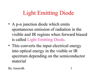
1. By Anurodh 1
Light Emitting Diode
• A p-n junction diode which emits
spontaneous emission of radiation in the
visible and IR regions when forward biased
is called Light Emitting Diode.
• This converts the input electrical energy
into optical energy in the visible or IR
spectrum depending on the semiconductor
material
2. By Anurodh 2
Light Emitting Diode
Working Principle:
The energy conversion takes place in two stages
1.The energy of carriers in the semiconductors is
raised above the equilibrium value by electrical
input energy
2.Most of these carriers after having lived a mean
life time in the higher energy state, give up their
energy as spontaneous emission of photons with
energy equal to bandgap Eg of the semiconductor.
3. By Anurodh 3
Choice of Materials
• The choice of semiconductor material
depends upon the required wavelength of
material in terms of their bandgap energy.
• Lower bandgap materials are required for IR
applications and energy band gaps greater
than or equal to about 2eV materials are
needed for a light in the visible part.
• The most important IV-V compounds are
binary compounds GaAs(bandgap= 1.43eV,
emission near IR region), GaP
(bandgap=2.26eV, red & green emission)
5. By Anurodh 5
Advantage of LED
• Simpler fabrication: There are no mirror facts
• Cost: The simpler construction of the LED leads to a
much reduced cost.
• Reliability: LED does not exhibit catastrophic
degradation and has proved far less sensitive to gradual
degradation than the injection laser.
• Less temperature dependence: The light output against
current is less affected by temperature than the
corresponding characteristic for the injection laser.
• Simpler drive circuitary: Temperature compensation
circuits are unnecessary as it can be operated in lower
drive currents and have reduced temperature
dependence.
• Linearity: As ideally the LED has a linear light output
against current characteristic unlike the injection laser
and advantageous where analog modulation is
considered.
6. By Anurodh 6
Differences between LED and Diode laser
• The output from the laser LED is incoherent,
whereas that from a diode laser is coherent.
• The light from an LED has a broad spectral width
and beam divergence and therefore information
carrying capacity of a system is much less.
• The light from a diode laser has both spatial and
temporal coherence and so is highly
monochromatic
• Diode laser is highly directional
• Coupling the LED to the fiber is more difficult
and the amount of power it can launch into the
fiber is relatively small.
• LED is less expensive compared to laser diodes.
7. By Anurodh 7
Light Emitting Diode (LED)
• The injected electrons and holes appear in
high concentrations in this transition region.
• At low forward current level, the electron-
hole recombinations cause spontaneous
emission of photons and the junction acts as
an LED. The band width of the emitted
light will be larger.
• As the current is increased, the intensity of
light increases linearly.
9. By Anurodh 9
Optical Detectors
• This is the most essential component of an
optical fiber communication system.
• Crucial in dictating the overall system
performance
• Converts optical signal, received from the
fiber, into electrical signal.
10. By Anurodh 10
Basic requirements of a photodetector
• Sensitivity at the required wavelength
• Efficient conversion of photons to electrons
• Fast response to operate at high frequencies
• Low noise for reduced errors
• Sufficient area for efficient coupling to
optical fiber
• High reliability capable of continuous stable
operation at room temperature
• Low cost
11. By Anurodh 11
PIN Photodiode
• The most common semiconductor
photodetector is the PIN photodiode
• Consists of p and n regions separated by a
very lightly n-doped intrinsic (i) region.
• Operated at sufficiently large reverse bias
voltage
• Under illumination the current varies almost
linearly with the incident light
12. By Anurodh 12
The pin Photodiode
pin energy-band diagram
pin photodiode circuit
13. By Anurodh 13
Construction
Cross-section view of a front-
illuminated sillicon p-i-n
photodiode.
•n-type material is doped so
lightly that it can be
considered intrinsic
•To make a low resistance
contact a highly doped n-
type (n+
) layer is added
•Front illuminated PIN
photodiode operates in the
0.8 to 0.9μm band
•To increase detection
efficiency antireflection
coatings are provided on the
front surfaces.
14. By Anurodh 14
Working
• In normal condition, the depletion region is formed by
immobile positively charged donor atoms in the n-type
semiconductor and immobile negatively charged acceptor
atoms in the p-type material.
• A large reverse bias voltage is applied across the device so
that the intrinsic region is fully depleted of charge carriers.
• When an incident photon has an energy greater than or
equal to bandgap energy of the semiconductor material, the
photon can give up its energy and excite an electron from
the valence band to the conduction band.
• This process generates free electron-hole pairs which are
known as photo carriers since they are photon generated
charge carriers.
15. By Anurodh 15
Working (contd…)
• The photodetector is normally designed so that these carriers are
generated mainly in the depletion region (the depleted intrinsic
region) where most of the incident light is absorbed.
• The high electric field present in the depletion region causes the
carriers to separate and be collected across the reverse biased
junction and gives rise to current flow in the external circuit.
This current flow is known as the photocurrent.
• On the average the charge carrriers move a distance Ln or
Lp for electrons and holes respectively. This distance is
known as diffusion length.
• The time it takes for an electron or hole to recombine is
known as carrier lifetime and is represented by Tn and Tp
respectively.
16. By Anurodh 16
PIN photodiode showing the combined
absorption and depletion region
17. By Anurodh 17
Working (contd…)
• A particular semiconductor material
canonly be used over a limited wavelength
range.
18. By Anurodh 18
Photodetectors
• Note: the absorption of photons occurs over a distance that
is dependant on wavelength. Remembering that the
distribution of the field is not uniform tells us that
determining the time dependence of the photocurrent
signal is difficult.
• The resultant photocurrent is a result of electron flow only
not hole migration.
• Integrating the hole current to calculate the Q charge will
show that the total photogenerated electrons is
(electrons) and not (electrons and holes).
eN
eN2