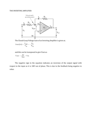
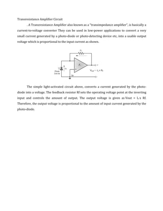
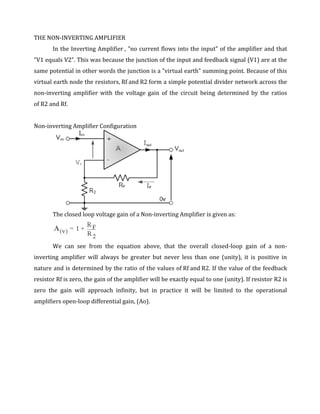
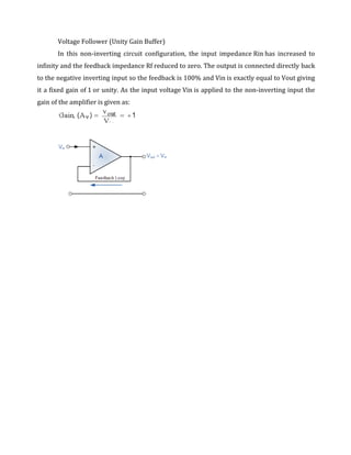
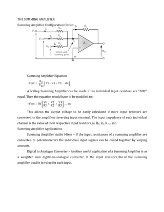
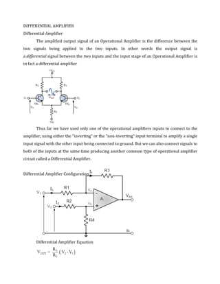
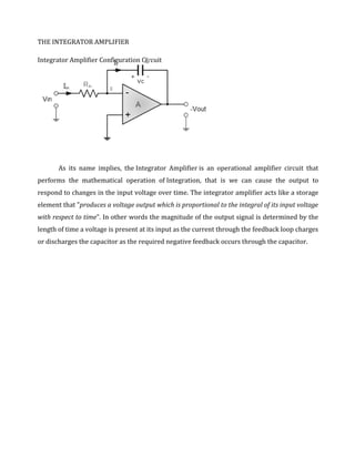
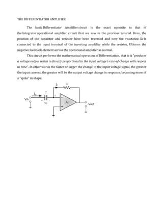
NATIONAL COLLEGE OF SCIENCE AND TECHNOLOGY
                          Amafel Building, Aguinaldo Highway Dasmariñas City, Cavite


                                       ASSIGNMENT # 1
                                   OPERATIONAL AMPLIFIER


Pagara, Sheila Marie P.                                               July 26, 2011
Electronics 3/BSECE 41A1                                              Score:


                                      Engr. Grace Ramones
                                           Instructor
OPERATIONAL AMPLIFIERS
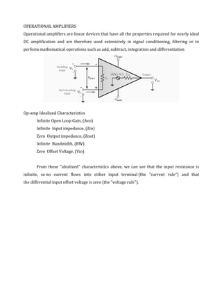
Operational amplifiers are linear devices that have all the properties required for nearly ideal
DC amplification and are therefore used extensively in signal conditioning, filtering or to
perform mathematical operations such as add, subtract, integration and differentiation


Op-amp Idealized Characteristics
       Infinite Open Loop Gain, (Avo)
       Infinite Input impedance, (Zin)
       Zero Output impedance, (Zout)
       Infinite Bandwidth, (BW)
       Zero Offset Voltage, (Vio)


       From these "idealized" characteristics above, we can see that the input resistance is
infinite, so no current flows into either input terminal (the "current rule") and that
the differential input offset voltage is zero (the "voltage rule").
Open-loop Frequency Response Curve of Op-amps


      An Operational Amplifiers Bandwidth
      The operational amplifiers bandwidth is the frequency range over which the voltage
gain of the amplifier is above 70.7% or -3dB (where 0dB is the maximum) of its maximum
output value as shown below.
THE INVERTING AMPLIFIER


         The Closed-Loop Voltage Gain of an Inverting Amplifier is given as.


         and this can be transposed to give Vout as:


         The negative sign in the equation indicates an inversion of the output signal with
respect to the input as it is 180o out of phase. This is due to the feedback being negative in
value.
Transresistance Amplifier Circuit
       . A Transresistance Amplifier also known as a "transimpedance amplifier", is basically a
current-to-voltage converter They can be used in low-power applications to convert a very
small current generated by a photo-diode or photo-detecting device etc, into a usable output
voltage which is proportional to the input current as shown.


       The simple light-activated circuit above, converts a current generated by the photo-
diode into a voltage. The feedback resistor Rf sets the operating voltage point at the inverting
input and controls the amount of output. The output voltage is given as Vout = Is x Rf.
Therefore, the output voltage is proportional to the amount of input current generated by the
photo-diode.
THE NON-INVERTING AMPLIFIER
       In the Inverting Amplifier , "no current flows into the input" of the amplifier and that
"V1 equals V2". This was because the junction of the input and feedback signal (V1) are at the
same potential in other words the junction is a "virtual earth" summing point. Because of this
virtual earth node the resistors, Rf and R2 form a simple potential divider network across the
non-inverting amplifier with the voltage gain of the circuit being determined by the ratios
of R2 and Rf.


Non-inverting Amplifier Configuration


       The closed loop voltage gain of a Non-inverting Amplifier is given as:


       We can see from the equation above, that the overall closed-loop gain of a non-
inverting amplifier will always be greater but never less than one (unity), it is positive in
nature and is determined by the ratio of the values of Rf and R2. If the value of the feedback
resistor Rf is zero, the gain of the amplifier will be exactly equal to one (unity). If resistor R2 is
zero the gain will approach infinity, but in practice it will be limited to the operational
amplifiers open-loop differential gain, (Ao).
Voltage Follower (Unity Gain Buffer)
       In this non-inverting circuit configuration, the input impedance Rin has increased to
infinity and the feedback impedance Rf reduced to zero. The output is connected directly back
to the negative inverting input so the feedback is 100% and Vin is exactly equal to Vout giving
it a fixed gain of 1 or unity. As the input voltage Vin is applied to the non-inverting input the
gain of the amplifier is given as:
THE SUMMING AMPLIFIER
Summing Amplifier Configuration Circuit


       Summing Amplifier Equation


       A Scaling Summing Amplifier can be made if the individual input resistors are "NOT"
equal. Then the equation would have to be modified to:


       This allows the output voltage to be easily calculated if more input resistors are
connected to the amplifiers inverting input terminal. The input impedance of each individual
channel is the value of their respective input resistors, ie, R1, R2, R3 ... etc.
Summing Amplifier Applications
       Summing Amplifier Audio Mixer – If the input resistances of a summing amplifier are
connected to potentiometers the individual input signals can be mixed together by varying
amounts.
       Digital to Analogue Converter – Another useful application of a Summing Amplifier is as
a weighted sum digital-to-analogue converter. If the input resistors, Rin of the summing
amplifier double in value for each input.
DIFFERENTIAL AMPLIFIER
Differential Amplifier
       The amplified output signal of an Operational Amplifier is the difference between the
two signals being applied to the two inputs. In other words the output signal is
a differential signal between the two inputs and the input stage of an Operational Amplifier is
in fact a differential amplifier


       Thus far we have used only one of the operational amplifiers inputs to connect to the
amplifier, using either the "inverting" or the "non-inverting" input terminal to amplify a single
input signal with the other input being connected to ground. But we can also connect signals to
both of the inputs at the same time producing another common type of operational amplifier
circuit called a Differential Amplifier.


Differential Amplifier Configuration


       Differential Amplifier Equation
THE INTEGRATOR AMPLIFIER

Integrator Amplifier Configuration Circuit


       As its name implies, the Integrator Amplifier is an operational amplifier circuit that
performs the mathematical operation of Integration, that is we can cause the output to
respond to changes in the input voltage over time. The integrator amplifier acts like a storage
element that "produces a voltage output which is proportional to the integral of its input voltage
with respect to time". In other words the magnitude of the output signal is determined by the
length of time a voltage is present at its input as the current through the feedback loop charges
or discharges the capacitor as the required negative feedback occurs through the capacitor.
THE DIFFERENTIATOR AMPLIFIER

       The basic Differentiator Amplifier circuit      is   the   exact   opposite   to   that   of
the Integrator operational amplifier circuit that we saw in the previous tutorial. Here, the
position of the capacitor and resistor have been reversed and now the reactance, Xc is
connected to the input terminal of the inverting amplifier while the resistor, Rf forms the
negative feedback element across the operational amplifier as normal.
       This circuit performs the mathematical operation of Differentiation, that is it "produces
a voltage output which is directly proportional to the input voltage's rate-of-change with respect
to time". In other words the faster or larger the change to the input voltage signal, the greater
the input current, the greater will be the output voltage change in response, becoming more of
a "spike" in shape.
Improved Differentiator Amplifier


       Adding the input resistor Rin limits the differentiators increase in gain at a ratio
of Rf/Rin. The circuit now acts like a differentiator amplifier at low frequencies and an
amplifier with resistive feedback at high frequencies giving much better noise rejection.
Additional attenuation of higher frequencies is accomplished by connecting a capacitor C1 in
parallel with the differentiator feedback resistor, Rf. This then forms the basis of a Active High
Pass Filter.

Pagra

  • 1.
    NATIONAL COLLEGE OFSCIENCE AND TECHNOLOGY Amafel Building, Aguinaldo Highway Dasmariñas City, Cavite ASSIGNMENT # 1 OPERATIONAL AMPLIFIER Pagara, Sheila Marie P. July 26, 2011 Electronics 3/BSECE 41A1 Score: Engr. Grace Ramones Instructor
  • 2.
    OPERATIONAL AMPLIFIERS Operational amplifiersare linear devices that have all the properties required for nearly ideal DC amplification and are therefore used extensively in signal conditioning, filtering or to perform mathematical operations such as add, subtract, integration and differentiation Op-amp Idealized Characteristics Infinite Open Loop Gain, (Avo) Infinite Input impedance, (Zin) Zero Output impedance, (Zout) Infinite Bandwidth, (BW) Zero Offset Voltage, (Vio) From these "idealized" characteristics above, we can see that the input resistance is infinite, so no current flows into either input terminal (the "current rule") and that the differential input offset voltage is zero (the "voltage rule").
  • 3.
    Open-loop Frequency ResponseCurve of Op-amps An Operational Amplifiers Bandwidth The operational amplifiers bandwidth is the frequency range over which the voltage gain of the amplifier is above 70.7% or -3dB (where 0dB is the maximum) of its maximum output value as shown below.
  • 4.
    THE INVERTING AMPLIFIER The Closed-Loop Voltage Gain of an Inverting Amplifier is given as. and this can be transposed to give Vout as: The negative sign in the equation indicates an inversion of the output signal with respect to the input as it is 180o out of phase. This is due to the feedback being negative in value.
  • 5.
    Transresistance Amplifier Circuit . A Transresistance Amplifier also known as a "transimpedance amplifier", is basically a current-to-voltage converter They can be used in low-power applications to convert a very small current generated by a photo-diode or photo-detecting device etc, into a usable output voltage which is proportional to the input current as shown. The simple light-activated circuit above, converts a current generated by the photo- diode into a voltage. The feedback resistor Rf sets the operating voltage point at the inverting input and controls the amount of output. The output voltage is given as Vout = Is x Rf. Therefore, the output voltage is proportional to the amount of input current generated by the photo-diode.
  • 6.
    THE NON-INVERTING AMPLIFIER In the Inverting Amplifier , "no current flows into the input" of the amplifier and that "V1 equals V2". This was because the junction of the input and feedback signal (V1) are at the same potential in other words the junction is a "virtual earth" summing point. Because of this virtual earth node the resistors, Rf and R2 form a simple potential divider network across the non-inverting amplifier with the voltage gain of the circuit being determined by the ratios of R2 and Rf. Non-inverting Amplifier Configuration The closed loop voltage gain of a Non-inverting Amplifier is given as: We can see from the equation above, that the overall closed-loop gain of a non- inverting amplifier will always be greater but never less than one (unity), it is positive in nature and is determined by the ratio of the values of Rf and R2. If the value of the feedback resistor Rf is zero, the gain of the amplifier will be exactly equal to one (unity). If resistor R2 is zero the gain will approach infinity, but in practice it will be limited to the operational amplifiers open-loop differential gain, (Ao).
  • 7.
    Voltage Follower (UnityGain Buffer) In this non-inverting circuit configuration, the input impedance Rin has increased to infinity and the feedback impedance Rf reduced to zero. The output is connected directly back to the negative inverting input so the feedback is 100% and Vin is exactly equal to Vout giving it a fixed gain of 1 or unity. As the input voltage Vin is applied to the non-inverting input the gain of the amplifier is given as:
  • 8.
    THE SUMMING AMPLIFIER SummingAmplifier Configuration Circuit Summing Amplifier Equation A Scaling Summing Amplifier can be made if the individual input resistors are "NOT" equal. Then the equation would have to be modified to: This allows the output voltage to be easily calculated if more input resistors are connected to the amplifiers inverting input terminal. The input impedance of each individual channel is the value of their respective input resistors, ie, R1, R2, R3 ... etc. Summing Amplifier Applications Summing Amplifier Audio Mixer – If the input resistances of a summing amplifier are connected to potentiometers the individual input signals can be mixed together by varying amounts. Digital to Analogue Converter – Another useful application of a Summing Amplifier is as a weighted sum digital-to-analogue converter. If the input resistors, Rin of the summing amplifier double in value for each input.
  • 9.
    DIFFERENTIAL AMPLIFIER Differential Amplifier The amplified output signal of an Operational Amplifier is the difference between the two signals being applied to the two inputs. In other words the output signal is a differential signal between the two inputs and the input stage of an Operational Amplifier is in fact a differential amplifier Thus far we have used only one of the operational amplifiers inputs to connect to the amplifier, using either the "inverting" or the "non-inverting" input terminal to amplify a single input signal with the other input being connected to ground. But we can also connect signals to both of the inputs at the same time producing another common type of operational amplifier circuit called a Differential Amplifier. Differential Amplifier Configuration Differential Amplifier Equation
  • 10.
    THE INTEGRATOR AMPLIFIER IntegratorAmplifier Configuration Circuit As its name implies, the Integrator Amplifier is an operational amplifier circuit that performs the mathematical operation of Integration, that is we can cause the output to respond to changes in the input voltage over time. The integrator amplifier acts like a storage element that "produces a voltage output which is proportional to the integral of its input voltage with respect to time". In other words the magnitude of the output signal is determined by the length of time a voltage is present at its input as the current through the feedback loop charges or discharges the capacitor as the required negative feedback occurs through the capacitor.
  • 11.
    THE DIFFERENTIATOR AMPLIFIER The basic Differentiator Amplifier circuit is the exact opposite to that of the Integrator operational amplifier circuit that we saw in the previous tutorial. Here, the position of the capacitor and resistor have been reversed and now the reactance, Xc is connected to the input terminal of the inverting amplifier while the resistor, Rf forms the negative feedback element across the operational amplifier as normal. This circuit performs the mathematical operation of Differentiation, that is it "produces a voltage output which is directly proportional to the input voltage's rate-of-change with respect to time". In other words the faster or larger the change to the input voltage signal, the greater the input current, the greater will be the output voltage change in response, becoming more of a "spike" in shape.
  • 12.
    Improved Differentiator Amplifier Adding the input resistor Rin limits the differentiators increase in gain at a ratio of Rf/Rin. The circuit now acts like a differentiator amplifier at low frequencies and an amplifier with resistive feedback at high frequencies giving much better noise rejection. Additional attenuation of higher frequencies is accomplished by connecting a capacitor C1 in parallel with the differentiator feedback resistor, Rf. This then forms the basis of a Active High Pass Filter.