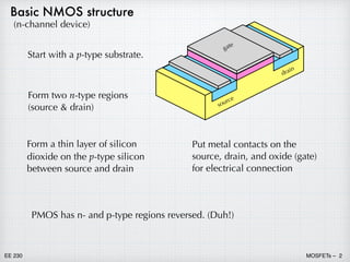
1) Metal oxide semiconductor field effect transistors (MOSFETs) have replaced bipolar junction transistors (BJTs) for most digital and some analog applications. MOSFETs use a metal oxide semiconductor structure to control current flow through an inversion layer between the source and drain using a gate voltage.
2) A p-channel MOSFET (PMOS) uses holes for current flow, while an n-channel MOSFET (NMOS) uses electrons. Combining NMOS and PMOS in complementary MOS (CMOS) circuits provides significant advantages in design.
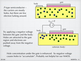
3) Applying different gate voltages results in either hole or electron accumulation at the semiconductor surface, depletion of carriers, or formation of an


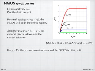
![EE 230 MOSFETs – 22
The mathematical analysis of what happens in a FET at pinch-off is a
fairly complicated problem in electromagnetics – definitely beyond
our current capabilities. (Again, see EE 332.)
However, the end result on the device behavior is easy to grasp – the
current saturates at the pinch down value. For higher values of vDS, the
current stays constant at a constant value.
The condition for the NMOS going reaching the “pinch-down”
condition is vGD ≤ VT. This can be re-expressed in terms of vDS and vGS.
To determine the saturation current, we can insert the pinch-down
condition given above into the iD-vDS equation from the ohmic region
of operation. Then the saturated current is
Y'6 Y*6 97
L' (VDW) =
ܟQR[
:
/
[Y*6 97]
= . [Y*6 97]
(Work out these details for yourself.)](https://image.slidesharecdn.com/nmos1-240206014513-1d6a6e1f/85/nmos-pdf-22-320.jpg)
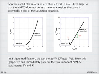
![EE 230 MOSFETs – 25
iD = 0
Summary of NMOS equations
The equations are exact (within the limits of the simplest MOSFET
model). The quadratic dependence of current on voltage means that
the circuit analysis will be non-linear and we will have frequent need
for the quadratic equation.
off
vGS VT
vGS ≥ VT on vDS vGS – VT ohmic or linear
vDS ≥ vGS – VT saturation
L' =
ܟQR[
:
/
(Y*6 97) Y'6 Y
'6
. =
ܟQR[
:
/
VT,
L' = . [Y*6 97]
iG = 0 !! (at least at DC)](https://image.slidesharecdn.com/nmos1-240206014513-1d6a6e1f/85/nmos-pdf-25-320.jpg)