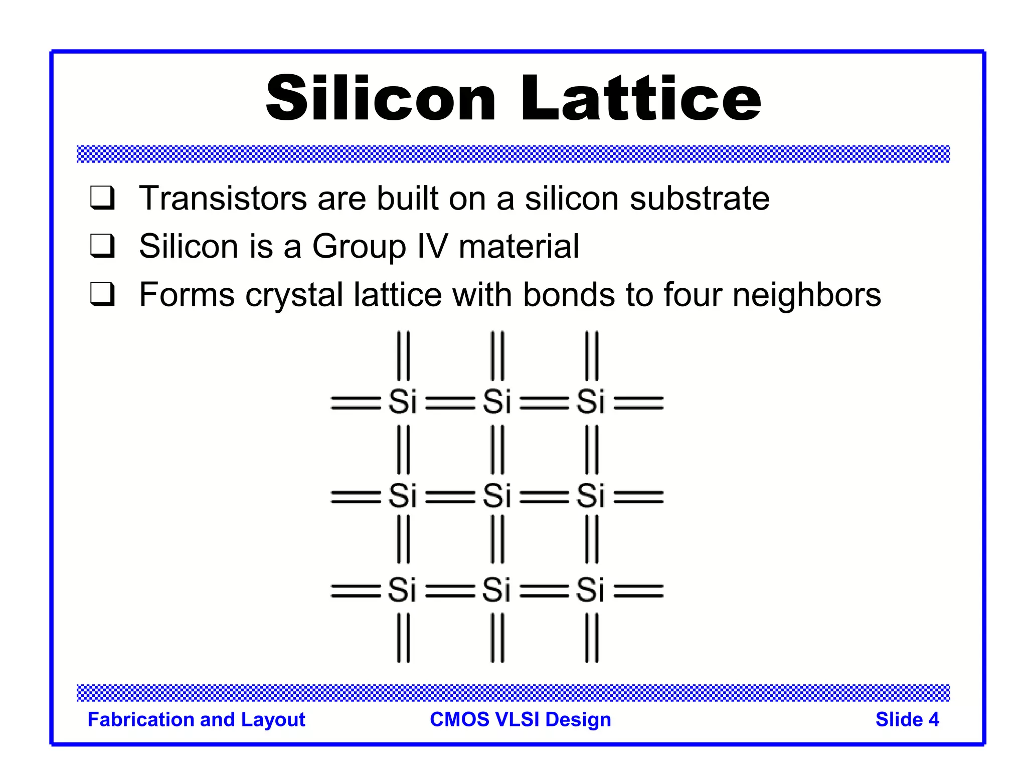
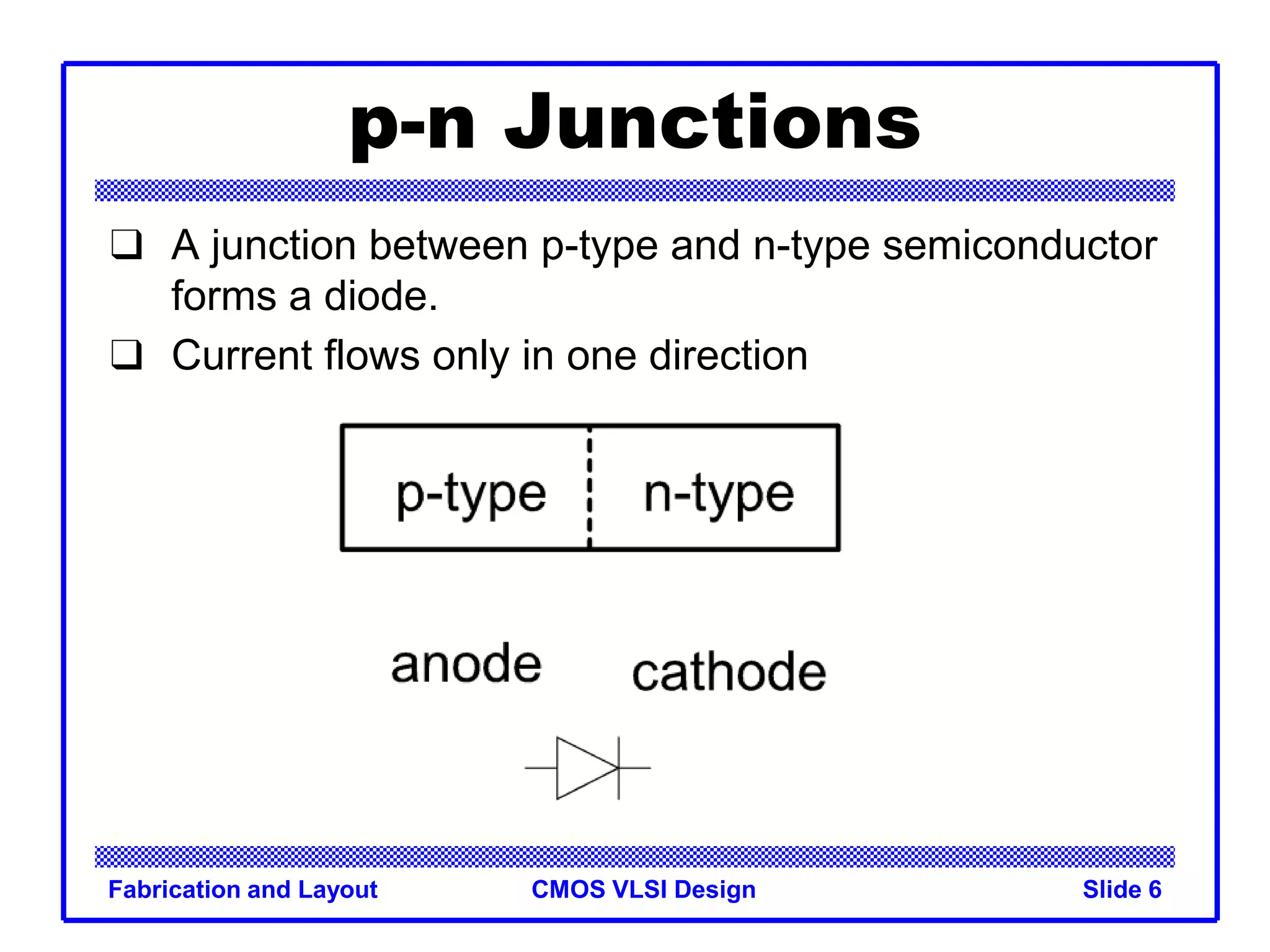
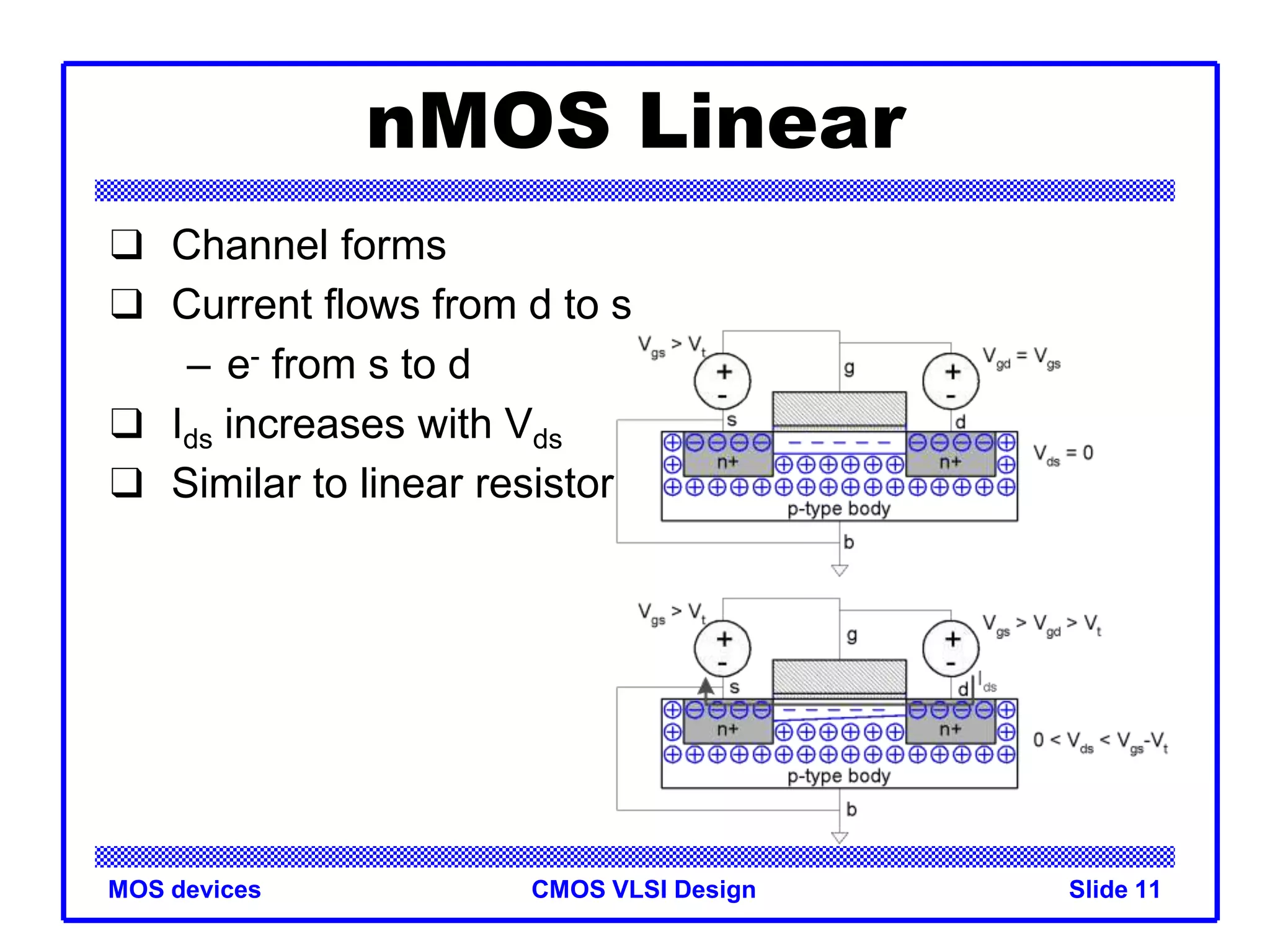
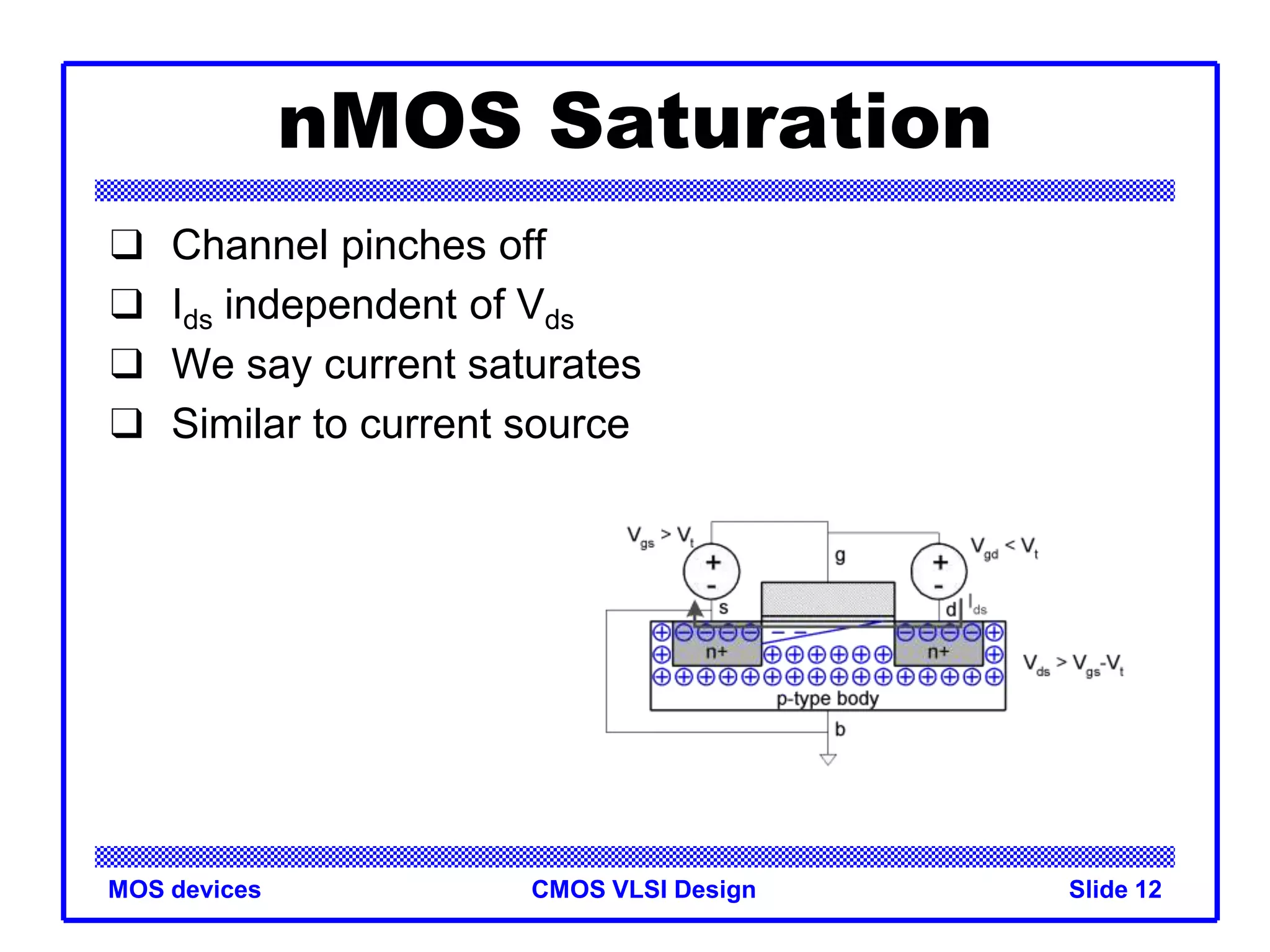
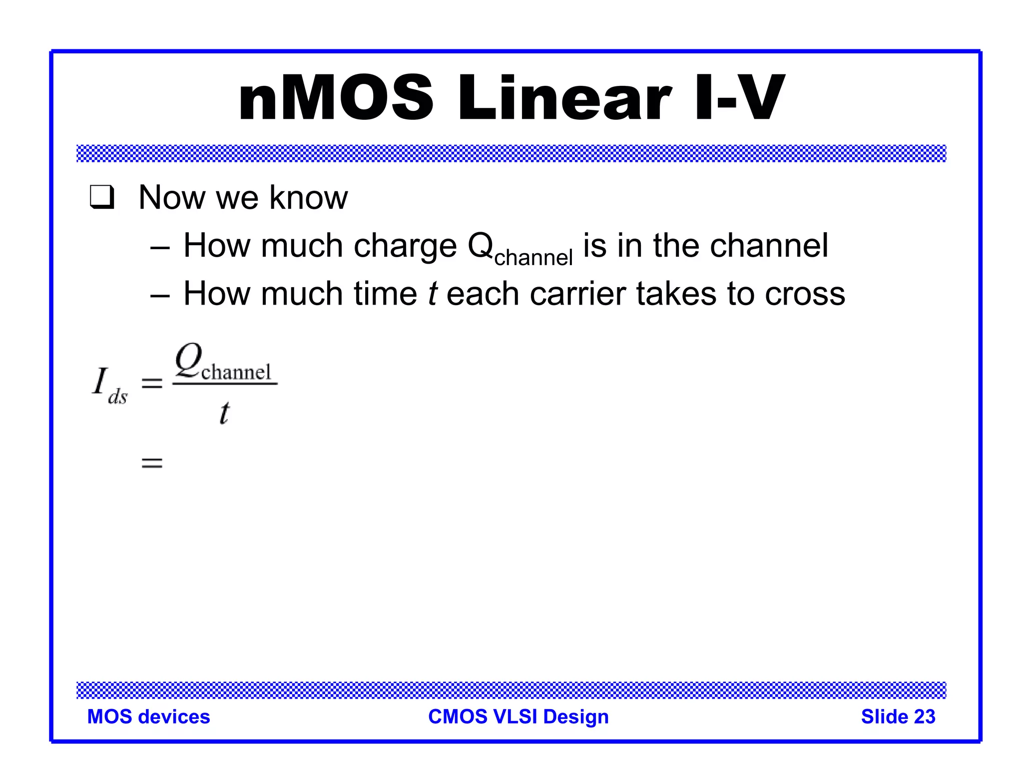
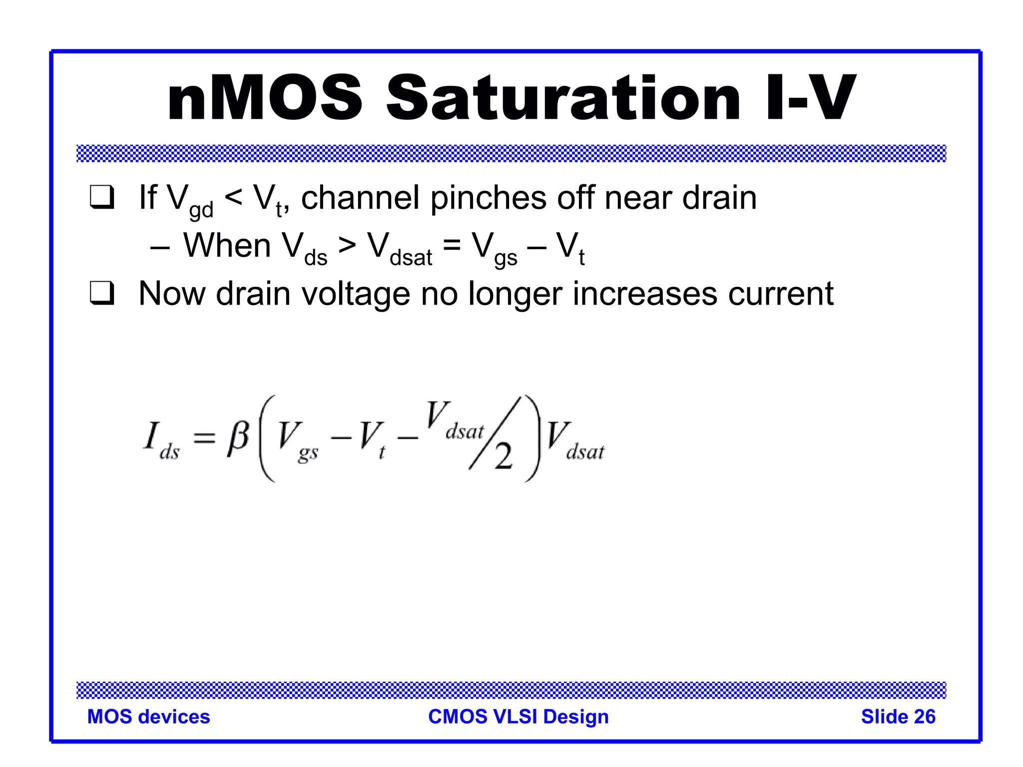
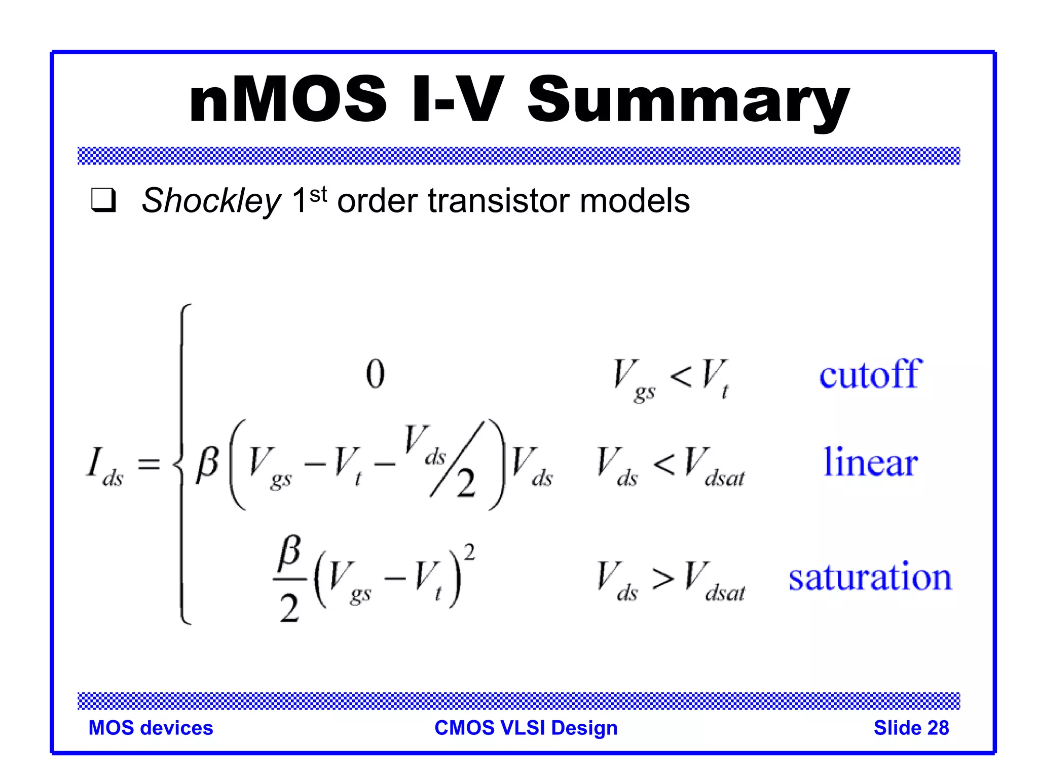
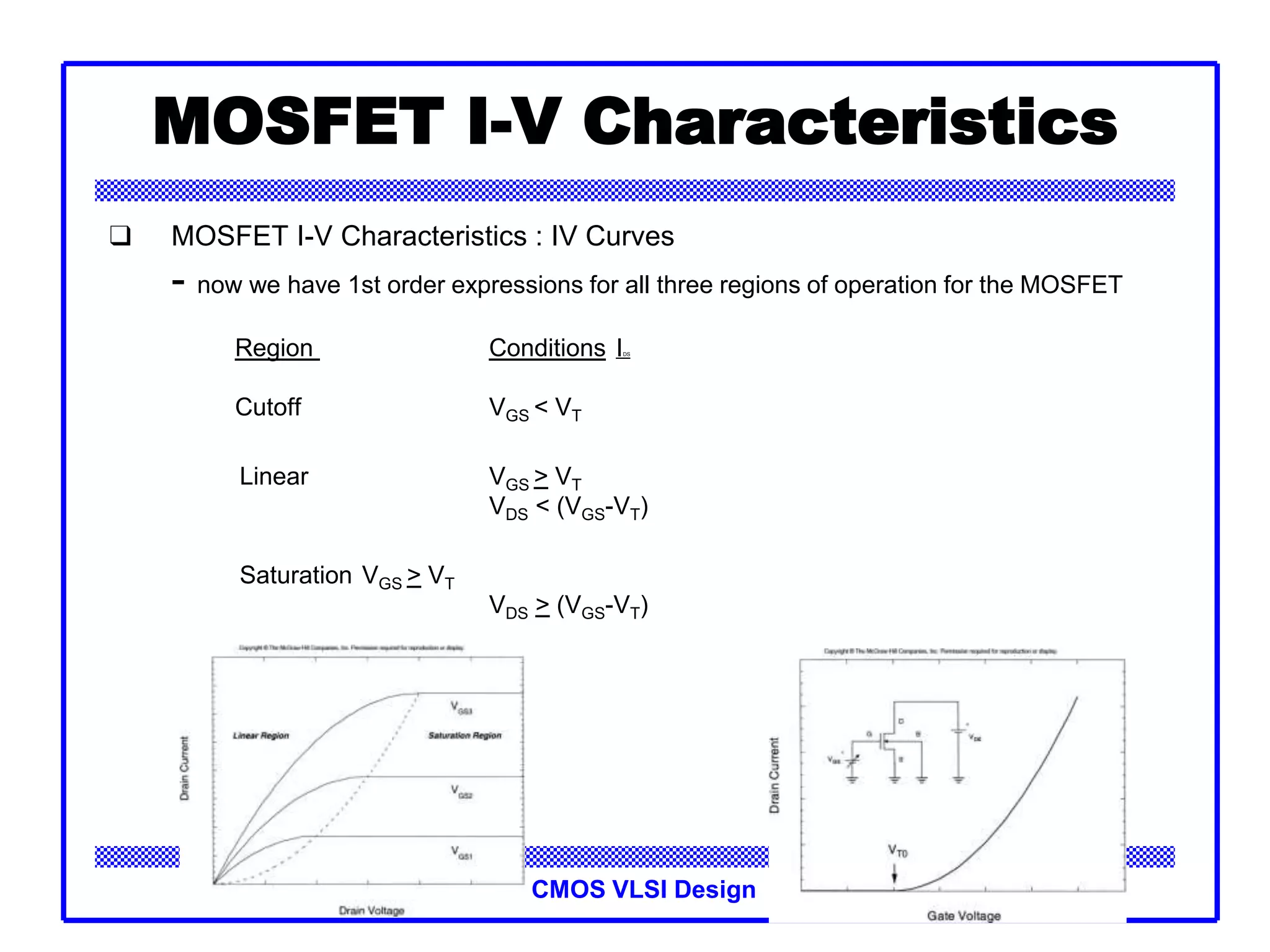
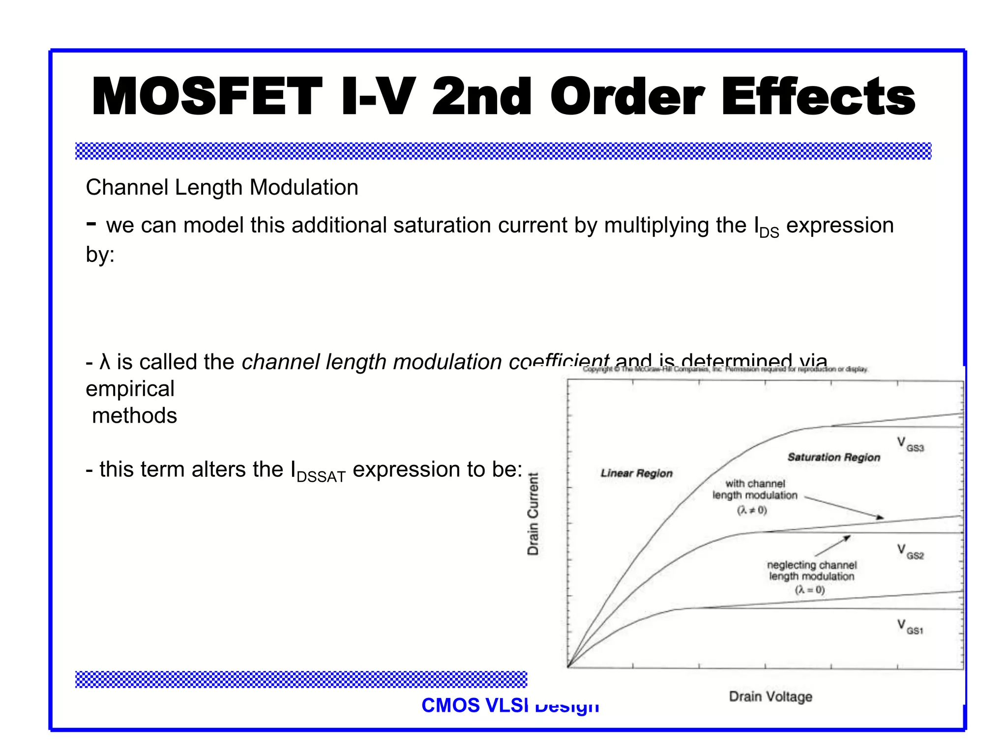
The document provides an introduction to CMOS VLSI design, covering MOS transistor theory and fabrication/layout. It discusses how MOS transistors are built on a silicon substrate using dopants to introduce carriers. The key modes of a MOS capacitor are described. Terminal voltages and regions of operation (cutoff, linear, saturation) for nMOS and pMOS transistors are explained. Equations are derived for channel charge, carrier velocity, and linear/saturation current-voltage characteristics. Second-order effects like channel length modulation and substrate bias are also covered.
3. CMOS VLSI Design
Fabrication and Layout Slide 3
Introduction
❑ Integrated circuits: many transistors on one chip.
– Very Large Scale Integration (VLSI): very many
❑ Metal Oxide Semiconductor (MOS) transistor
– Fast, cheap, low-power transistors
– Complementary: mixture of n- and p-type leads to
less power
❑ Today: How to build your own simple CMOS chip
– CMOS transistors
– Building logic gates from transistors
– Transistor layout and fabrication
❑ Rest of the course: How to build a good CMOS chip
4. CMOS VLSI Design
Fabrication and Layout Slide 4
Silicon Lattice
❑ Transistors are built on a silicon substrate
❑ Silicon is a Group IV material
❑ Forms crystal lattice with bonds to four neighbors
5. CMOS VLSI Design
Fabrication and Layout Slide 5
Dopants
❑ Silicon is a semiconductor
❑ Pure silicon has no free carriers and conducts poorly
❑ Adding dopants increases the conductivity
❑ Group V: extra electron (n-type)
❑ Group III: missing electron, called hole (p-type)
6. CMOS VLSI Design
Fabrication and Layout Slide 6
p-n Junctions
❑ A junction between p-type and n-type semiconductor
forms a diode.
❑ Current flows only in one direction
7. CMOS VLSI Design
MOS devices Slide 7
Introduction
❑ So far, we have treated transistors as ideal switches
❑ An ON transistor passes a finite amount of current
– Depends on terminal voltages
– Derive current-voltage (I-V) relationships
❑ Transistor gate, source, drain all have capacitance
– I = C (ΔV/Δt) -> Δt = (C/I) ΔV
– Capacitance and current determine speed
❑ Also explore what a “degraded level” really means
8. CMOS VLSI Design
MOS devices Slide 8
MOS Capacitor
❑ Gate and body form MOS capacitor
❑ Operating modes
– Accumulation
– Depletion
– Inversion
9. CMOS VLSI Design
MOS devices Slide 9
Terminal Voltages
❑ Mode of operation depends on Vg, Vd, Vs
– Vgs = Vg – Vs
– Vgd = Vg – Vd
– Vds = Vd – Vs = Vgs - Vgd
❑ Source and drain are symmetric diffusion terminals
– By convention, source is terminal at lower voltage
– Hence Vds ≥ 0
❑ nMOS body is grounded. First assume source is 0 too.
❑ Three regions of operation
– Cutoff
– Linear
– Saturation
11. CMOS VLSI Design
MOS devices Slide 11
nMOS Linear
❑ Channel forms
❑ Current flows from d to s
– e- from s to d
❑ Ids increases with Vds
❑ Similar to linear resistor
12. CMOS VLSI Design
MOS devices Slide 12
nMOS Saturation
❑ Channel pinches off
❑ Ids independent of Vds
❑ We say current saturates
❑ Similar to current source
13. CMOS VLSI Design
MOS devices Slide 13
I-V Characteristics
❑ In Linear region, Ids depends on
– How much charge is in the channel?
– How fast is the charge moving?
14. CMOS VLSI Design
MOS devices Slide 14
Channel Charge
❑ MOS structure looks like parallel plate capacitor
while operating in inversion
– Gate – oxide – channel
❑ Qchannel =
15. CMOS VLSI Design
MOS devices Slide 15
Channel Charge
❑ MOS structure looks like parallel plate capacitor
while operating in inversion
– Gate – oxide – channel
❑ Qchannel = CV
❑ C =
16. CMOS VLSI Design
MOS devices Slide 16
Channel Charge
❑ MOS structure looks like parallel plate capacitor
while operating in inversion
– Gate – oxide – channel
❑ Qchannel = CV
❑ C = Cg = εoxWL/tox = CoxWL
❑ V =
Cox = εox / tox
17. CMOS VLSI Design
MOS devices Slide 17
Channel Charge
❑ MOS structure looks like parallel plate capacitor
while operating in inversion
– Gate – oxide – channel
❑ Qchannel = CV
❑ C = Cg = εoxWL/tox = CoxWL
❑ V = Vgc – Vt = (Vgs – Vds/2) – Vt
Cox = εox / tox
18. CMOS VLSI Design
MOS devices Slide 18
Carrier velocity
❑ Charge is carried by e-
❑ Carrier velocity v proportional to lateral E-field
between source and drain
❑ v =
19. CMOS VLSI Design
MOS devices Slide 19
Carrier velocity
❑ Charge is carried by e-
❑ Carrier velocity v proportional to lateral E-field
between source and drain
❑ v = μE μ called mobility
❑ E =
20. CMOS VLSI Design
MOS devices Slide 20
Carrier velocity
❑ Charge is carried by e-
❑ Carrier velocity v proportional to lateral E-field
between source and drain
❑ v = μE μ called mobility
❑ E = Vds/L
❑ Time for carrier to cross channel:
– t =
21. CMOS VLSI Design
MOS devices Slide 21
Carrier velocity
❑ Charge is carried by e-
❑ Carrier velocity v proportional to lateral E-field
between source and drain
❑ v = μE μ called mobility
❑ E = Vds/L
❑ Time for carrier to cross channel:
– t = L / v
22. CMOS VLSI Design
MOS devices Slide 22
nMOS Linear I-V
❑ Now we know
– How much charge Qchannel is in the channel
– How much time t each carrier takes to cross
23. CMOS VLSI Design
MOS devices Slide 23
nMOS Linear I-V
❑ Now we know
– How much charge Qchannel is in the channel
– How much time t each carrier takes to cross
24. CMOS VLSI Design
MOS devices Slide 24
nMOS Linear I-V
❑ Now we know
– How much charge Qchannel is in the channel
– How much time t each carrier takes to cross
25. CMOS VLSI Design
MOS devices Slide 25
nMOS Saturation I-V
❑ If Vgd < Vt, channel pinches off near drain
– When Vds > Vdsat = Vgs – Vt
❑ Now drain voltage no longer increases current
26. CMOS VLSI Design
MOS devices Slide 26
nMOS Saturation I-V
❑ If Vgd < Vt, channel pinches off near drain
– When Vds > Vdsat = Vgs – Vt
❑ Now drain voltage no longer increases current
27. CMOS VLSI Design
MOS devices Slide 27
nMOS Saturation I-V
❑ If Vgd < Vt, channel pinches off near drain
– When Vds > Vdsat = Vgs – Vt
❑ Now drain voltage no longer increases current
28. CMOS VLSI Design
MOS devices Slide 28
nMOS I-V Summary
❑ Shockley 1st order transistor models
29. CMOS VLSI Design
MOS devices Slide 29
Example
❑ Example: a 0.6 μm process from AMI semiconductor
– tox = 100 Å
– μ = 350 cm2/V*s
– Vt = 0.7 V
❑ Plot Ids vs. Vds
– Vgs = 0, 1, 2, 3, 4, 5
– Use W/L = 4/2 λ
30. CMOS VLSI Design
MOS devices Slide 30
pMOS I-V
❑ All dopings and voltages are inverted for pMOS
❑ Mobility μp is determined by holes
– Typically 2-3x lower than that of electrons μn
– 120 cm2/V*s in AMI 0.6 μm process
❑ Thus pMOS must be wider to provide same current
– In this class, assume μn / μp = 2
31. CMOS VLSI Design
MOS devices Slide 31
Capacitance
❑ Any two conductors separated by an insulator have
capacitance
❑ Gate to channel capacitor is very important
– Creates channel charge necessary for operation
❑ Source and drain have capacitance to body
– Across reverse-biased diodes
– Called diffusion capacitance because it is
associated with source/drain diffusion
32. CMOS VLSI Design
MOS devices Slide 32
Gate Capacitance
❑ Approximate channel as connected to source
❑ Cgs = εoxWL/tox = CoxWL = CpermicronW
❑ Cpermicron is typically about 2 fF/μm
33. CMOS VLSI Design
MOS devices Slide 33
Diffusion Capacitance
❑ Csb, Cdb
❑ Undesirable, called parasitic capacitance
❑ Capacitance depends on area and perimeter
– Use small diffusion nodes
– Comparable to Cg
for contacted diff
– ½ Cg for uncontacted
– Varies with process
34. CMOS VLSI Design
MOSFET I-V Characteristics
❑ MOSFET I-V Characteristics : IV Curves
- now we have 1st order expressions for all three regions of operation for the MOSFET
Region Conditions IDS
Cutoff VGS < VT
Linear VGS > VT
VDS < (VGS-VT)
Saturation VGS > VT
VDS > (VGS-VT)
35. CMOS VLSI Design
MOSFET I-V 2nd Order Effects
❑Channel Length Modulation
- the 1st order IV equations derived earlier are not 100% accurate. They are sufficient for 1st
order (gut-feel) hand calculations
- we can modify these IV equations to include other effects that alter the IV characteristics of a
MOSFET
- Channel Length Modulation refers to additional IDS current that exists in the saturation mode
that is not modeled by the 1st order IV equations
- when the channel is pinched off in saturation
by a distance ΔL, a depletion region is created
next to the Drain that is ΔL wide
- given enough energy, electrons in the inversion
layer can move through this depletion region
and into the Drain thus adding additional
current to IDS
36. CMOS VLSI Design
MOSFET I-V 2nd Order Effects
Channel Length Modulation
- we can model this additional saturation current by multiplying the IDS expression
by:
- λ is called the channel length modulation coefficient and is determined via
empirical
methods
- this term alters the IDSSAT expression to be:
37. CMOS VLSI Design
MOSFET I-V 2nd Order Effects
Substrate Bias Effect
- another effect that the 1st order IV equations don't model is substrate bias
- we have assumed that the Silicon substrate is at the same potential as the Source of
the MOSFET
- if this is not the case, then the Threshold Voltage may increase and take more energy
to induce a channel
- we've already seen how we can model the change in threshold voltage due to
substrate bias:
- for the IV equations to accurately model the substrate bias effect, we must use
VT instead of VT0