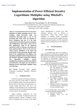
Implementation of Power Efficient Iterative
Logarithmic Multiplier using Mitchell’s
Algorithm
1
Kavya Shree M S, 2
Praveen Kumar Y G, 3
Dr. M Z Kurian
1
4th
sem, M.Tech (VLSI and Embedded Systems ), SSIT, Tumakuru (kavyabhramara5@gmail.com)
2
Asst. Prof, Dept. of ECE, SSIT, Tumakuru
3
HOD, Dept. of ECE, SSIT, Tumakuru
Abstract: As the demand increases for low power
dissipation in digital computing system, a new
technique called Reversible Logic was
introduced. Reversible logic is one of the
promising field which solves the problem of
power dissipation and also it is the basic
requirement for the field of quantum computing.
The multiplication which plays a prior role in
DSP applications. Some of the important
operations in DSP are filtering, convolution and
inner partial products. These are the processes
which requires multipliers so the speed and
performance of their operations depends on the
speed of the multiplication and addition. The
logarithmic multiplier which is designed based on
the Mitchell’s Algorithm proposed by Mitchell.
The logarithmic multiplier convert
multiplication and division problem into addition
and subtraction. This paper gives the design of
pipelined iterative logarithmic multiplier using
reversible logic.
Key Words: Reversible Logic, quantum
Computing, Logarithmic Multiplier, Mitchell’s
Algorithm.
I. INTRODUCTION:
Reversible Logic has received great attention in
the recent years due to their ability to reduce the
power dissipation which is the main requirement in
the low power VLSI design. Reversible logic is an
n-input n-output logic device with one to one
mapping. In the designing of the reversible logic
circuits direct fan-out is not allowed and the concept
of one-to-many is not entertained.
Digital arithmetic calculations are most
important in the design of digital processors and
application-specific systems. Arithmetic circuits
plays an important class of circuits in the digital
system. Multiplication is relevant since other
arithmetic operators such as division or
exponentiation, which they usually utilize
multipliers as building blocks. Logarithmic
multiplier converts given binary numbers into their
equivalent logarithm numbers. In LNS (Logarithmic
Number System) multiplication is done interms of
addition.
II. SYSTEM DESIGN:
i. Reversible Logic:
A reversible logic gate is an n-input, n-
output logic device with one-to-one mapping, which
helps to retrieve the inputs from the outputs. Also in
the synthesis of reversible circuits direct fan-out is
not allowed as one-to-many concept is not
reversible. However fan-out in reversible circuits is
achieved using additional gates.
There are many parameters for determining
the complexity and performance of circuits.
 The number of reversible gates
(N): The number of reversible
gates used in the circuits.
 The number of constant inputs
(CI): The number of inputs that
are maintained constant at either 0
or 1in order to synthesize the
given logical function.
 The number of garbage outputs
(GO): The number of unused
outputs present in a reversible
logic circuits.
 Quantum cost (QC): The quantum
cost refers to the cost of the circuit
in terms of primitive gates.
In a reversible logic circuit design two
restrictions should be maintain strictly.
 Fan-out is not allowed.
 Feedback loops are also
prohibited.
ISBN-13: 978-1535448697
www.iaetsd.in
Proceedings of ICRMET-2016
©IAETSD 201650
Logic synthesis of reversible logic circuits
should have the following objectives to achieve
optimized structure.
 Design should use minimum
number of logic gates.
 Constant inputs should be
minimum.
 Quantum cost should be kept as
low as possible.
III. PROPOSED SYSTEM DESIGN
A basic block (BB) is the proposed multiplier
with no correction terms. It calculates one
approximate product. The basic block is presented in
Figure 1, which consists of two leading-one
detectors (LODs), two encoders, two barrel shifters,
and decode unit decodes k1 + k2, i.e. it puts the
leading one in the product. The left shifters are used
to shift the residues. The two shifted residues are
then added to form the approximate product.
Figure 1: Basic Block Diagram of the Proposed
Logarithmic Multiplier.
1. Leading One Detector:
The implementation of the 4-bit LOD unit
is presented in Figure 2. The LOD units are used to
detect the leading one from the operands, which are
then passed to the barrel shifters. For 4-bit binary
number, i =3 indicates the MSB bit, the algorithm
checks if there is a one in that place. If there is a one
then it will pass the one followed by zeros. Else it
checks the next MSB place and so on until a leading
one is detected.
Figure 2: Flow Diagram of Leading-One
Detector (LOD)
2. Priority Encoder:
A priority encoder is a circuit or algorithm
that compresses multiple binary inputs into a small
number of outputs is as shown in Figure 3. The
output of a priority encoder is a binary
representation of the ordinal number starting from
zero of the most significant input bit. They are often
used to control interrupt requests by acting on the
highest priority request.
Figure 3: Block Diagram and Truth Table
of Priority Encoder.
3. Adder:
An adder or summer is a digital circuit
that performs addition of numbers. Ripple carry
adder shown in Figure 4, is used in proposed
multiplier.
Figure 4: Block Diagram of the Ripple Carry
Adder.
ISBN-13: 978-1535448697
www.iaetsd.in
Proceedings of ICRMET-2016
©IAETSD 201651
4. XOR Gate:
The XOR gate is a digital logic gate that
implements an exclusive or; that is, a true output (1)
results if one and only one of the inputs to the gate
is true (1). If both inputs are false (0) and both are
true (1), a false output (0) results. The block diagram
of XOR gate is as shown in Figure 5. XOR is "one
or the other but not both".
Figure 5: Block Diagram of XOR gate.
5. Decoder:
Decoder is a multiple input, multiple output
logic circuit which converts coded inputs into coded
outputs, where the input and output codes are
different shown in Figure 6.
Figure 6: Block Diagram of Decoder.
Implementation with Correction Circuits
The basic block is used in subsequent
implementations to implement correction circuits
and increase the accuracy of the multiplier. The
error-correction circuit is used to calculate the term
C (1)
and thus approximates the term (N1 - 2k1
) (N2 -
2k2
).To implements the proposed multipliers,
cascade the basic blocks. A block diagram of the
proposed logarithmic multiplier with one error
correction circuit is shown in Figure 7. The
multiplier is composed of two basic blocks, of which
the first one calculates the first approximation of the
product P(0)
approx., while the second one calculates
the error-correction term C(1)
.
Figure 7: Block Diagram of the Proposed
Multiplier with Error Correction Circuit.
The implementation with correction
circuits shows substantial increase in combinational
delay as each correction circuit is added. The two
basic blocks cannot really work in parallel in real-
time, because the correction block cannot start until
the residues are calculated from the first basic block.
But in the pipelined implementation of the basic
block the residues are available after the first stage;
the correction circuit can start to work immediately
after the first stage from the prior block is finished.
IV. IMPLEMENTATION OF PROPOSED
MULTIPLIER
The RTL schematic of 4X4 reversible
logarithmic multiplier without correction circuit is
as shown in Figure 8.
Figure 8: RTL Schematic of Reversible Log
Multiplier Without Correction Terms.
ISBN-13: 978-1535448697
www.iaetsd.in
Proceedings of ICRMET-2016
©IAETSD 201652
The RTL schematic of iterative 4X4
reversible logarithmic multiplier with correction
circuit is as shown in Figure 9
.
Figure 9: RTL Schematic of Reversible Log
Multiplier With 7 Correction Terms.
The reversible implementation and
simulation result of logarithmic multiplier is as
shown in Figure 10.
Figure 10: Simulation Result of 4X4 Reversible
Log Multiplier.
CONCLUSION
In this paper, the 4X4 reversible
logarithmic multiplier is designed with less number
of LUT slices.
Logarithmic multiplier is designed and
implemented on Spartan-6 FPGA board using Xilinx
14.5 ISE tool. It is observed that, reversible logic is
the better solutions for the designing of logarithmic
multiplier with the better optimization of the power.
As a future work, this design can be used
for image enhancement, image compression, video
tracking, DSP filters etc..
REFERENCES
[1]Z. Babi’c, A.Avramovi’c, P. Buli’c, “An iterative
logarithmic multiplier” ELSEVIER
publication 2011, pp. 0141-9331.
[2]Landauer .R, “Irreversibility and heat generation
in the computing process”, IBM Research and
Development, pp.183-191, 1961.
[3]Bennett C.H., “Logical reversiblility of
Computatio”, IBM Research and Development,
pp 525-532, 1973.
[4]P.Vanusha, k.AmruthaVally, “Low Power
Computing Logic Gate design using Reversible
logic”, International Journal of Application or
Innovation in Engineering & Management, Vol.
3, N0. 10, pp. 2319-4847, OCT 2014.
[5]Ravish Aradhya H.V, Lakshmesha J,
Muralidhara K.N, “Design optimization of
Reversible Logic Universal Barrel Shifter for
Low Power applications”, International Journal
of Computer Applications, Vol. 40, No. 15, pp.
0975-8887, Feb 2012.
[6] P.K.Lala, J.P.Parkson, P.Chakraborty, “Adder
Designs using Reversible Logic Gates”, WSEAS
transaction on circuits and systems, Vol. 9, No.
6, ISSN 1109-2734, June 2010.
[7] Sanjeev Kumar Patel, Vinod Kapse, “Optimized
Design and Implementation of an Iterative
Logarithmic Signed Multiplier”, International
Journal of Scientific & Engineering Research,
Vol. 3, No. 13, pp. 2229-5518, Dec 2012.
[8]Bhavani Prasad.Y, Rajeev Pankaj.N,
Samhitha.N.R, Shruthi.U.K, “Design of
Reversible Multiplier by Novel ANU gate”,
International Journal of Engineering and
Technology, Vol. 4, No, 6, pp. 2049-3444, June
2014.
[9] Pragyan Paramita Mohantly1, Mrs.Annapurana
K.Y.2, “FPGA Implementation of Iterative Log
Multiplier using Operand Decomposition for
Image Processing Application”, International
Journal for Research in Applied Science and
Engineering Technology, Vol. 2, No. 6, pp.
2321-9653, June 2014.
[10] Patricio Buli’c*, Zdenka Babi’c and Aleksej
Avramovi’c, “A Simple Pipelined Logarithmic
ISBN-13: 978-1535448697
www.iaetsd.in
Proceedings of ICRMET-2016
©IAETSD 201653
Multiplier”, IEEE Transactions on Computers,
pp. 978-1-4244-8935, Oct 2010.
[11] Arindam Banerjee*, Samayita Sankar, Mainuck
Das and Aniruddha Ghosh, “Design of
Reversible binary Logarithmic Multiplier and
Divider using Optimal Harbage”, International
Journal of Advanced Computer Research, Vol.
5, No. 18. pp. 2277-7970, March 2015.
[12] Rakshith.T.R, Rakshith Saligram, “Design of
High Speed Low Power Multiplier using
Reversible Logic: a Vedic Mathematical
Approach”, International Conference on
Circuits, Power and Computing Technologies,
pp. 4673-492, ICCPCT-2013.
[13] Kavyashree M S, Praveen Kumar Y G, Dr M Z
Kurian, “Design and Implementation of 4x4
Pipelined Iterative Logarithmic Multiplier
using Reversible Logic”, proceedings of
International Conference on Signal Processing,
Communication and Computational
Research(ICSPCCR-16),
ISBN:9788192958041, Pages:113, May 2016.
[14] Kavyashree M S, Praveen Kumar Y G, Dr M Z
Kurian, “A survey on Reversible Logic based
Logarithmic Multipliers”, proceedings of
National Conference on Recent Trends in
Information and Communication
Technology(NCRTICT-2016), ISBN: 978-81-
927765-3-8, PP:40-42, April 2016.
ISBN-13: 978-1535448697
www.iaetsd.in
Proceedings of ICRMET-2016
©IAETSD 201654

Iaetsd implementation of power efficient iterative logarithmic multiplier using mitchell’s

  • 1.
    Implementation of PowerEfficient Iterative Logarithmic Multiplier using Mitchell’s Algorithm 1 Kavya Shree M S, 2 Praveen Kumar Y G, 3 Dr. M Z Kurian 1 4th sem, M.Tech (VLSI and Embedded Systems ), SSIT, Tumakuru (kavyabhramara5@gmail.com) 2 Asst. Prof, Dept. of ECE, SSIT, Tumakuru 3 HOD, Dept. of ECE, SSIT, Tumakuru Abstract: As the demand increases for low power dissipation in digital computing system, a new technique called Reversible Logic was introduced. Reversible logic is one of the promising field which solves the problem of power dissipation and also it is the basic requirement for the field of quantum computing. The multiplication which plays a prior role in DSP applications. Some of the important operations in DSP are filtering, convolution and inner partial products. These are the processes which requires multipliers so the speed and performance of their operations depends on the speed of the multiplication and addition. The logarithmic multiplier which is designed based on the Mitchell’s Algorithm proposed by Mitchell. The logarithmic multiplier convert multiplication and division problem into addition and subtraction. This paper gives the design of pipelined iterative logarithmic multiplier using reversible logic. Key Words: Reversible Logic, quantum Computing, Logarithmic Multiplier, Mitchell’s Algorithm. I. INTRODUCTION: Reversible Logic has received great attention in the recent years due to their ability to reduce the power dissipation which is the main requirement in the low power VLSI design. Reversible logic is an n-input n-output logic device with one to one mapping. In the designing of the reversible logic circuits direct fan-out is not allowed and the concept of one-to-many is not entertained. Digital arithmetic calculations are most important in the design of digital processors and application-specific systems. Arithmetic circuits plays an important class of circuits in the digital system. Multiplication is relevant since other arithmetic operators such as division or exponentiation, which they usually utilize multipliers as building blocks. Logarithmic multiplier converts given binary numbers into their equivalent logarithm numbers. In LNS (Logarithmic Number System) multiplication is done interms of addition. II. SYSTEM DESIGN: i. Reversible Logic: A reversible logic gate is an n-input, n- output logic device with one-to-one mapping, which helps to retrieve the inputs from the outputs. Also in the synthesis of reversible circuits direct fan-out is not allowed as one-to-many concept is not reversible. However fan-out in reversible circuits is achieved using additional gates. There are many parameters for determining the complexity and performance of circuits.  The number of reversible gates (N): The number of reversible gates used in the circuits.  The number of constant inputs (CI): The number of inputs that are maintained constant at either 0 or 1in order to synthesize the given logical function.  The number of garbage outputs (GO): The number of unused outputs present in a reversible logic circuits.  Quantum cost (QC): The quantum cost refers to the cost of the circuit in terms of primitive gates. In a reversible logic circuit design two restrictions should be maintain strictly.  Fan-out is not allowed.  Feedback loops are also prohibited. ISBN-13: 978-1535448697 www.iaetsd.in Proceedings of ICRMET-2016 ©IAETSD 201650
  • 2.
    Logic synthesis ofreversible logic circuits should have the following objectives to achieve optimized structure.  Design should use minimum number of logic gates.  Constant inputs should be minimum.  Quantum cost should be kept as low as possible. III. PROPOSED SYSTEM DESIGN A basic block (BB) is the proposed multiplier with no correction terms. It calculates one approximate product. The basic block is presented in Figure 1, which consists of two leading-one detectors (LODs), two encoders, two barrel shifters, and decode unit decodes k1 + k2, i.e. it puts the leading one in the product. The left shifters are used to shift the residues. The two shifted residues are then added to form the approximate product. Figure 1: Basic Block Diagram of the Proposed Logarithmic Multiplier. 1. Leading One Detector: The implementation of the 4-bit LOD unit is presented in Figure 2. The LOD units are used to detect the leading one from the operands, which are then passed to the barrel shifters. For 4-bit binary number, i =3 indicates the MSB bit, the algorithm checks if there is a one in that place. If there is a one then it will pass the one followed by zeros. Else it checks the next MSB place and so on until a leading one is detected. Figure 2: Flow Diagram of Leading-One Detector (LOD) 2. Priority Encoder: A priority encoder is a circuit or algorithm that compresses multiple binary inputs into a small number of outputs is as shown in Figure 3. The output of a priority encoder is a binary representation of the ordinal number starting from zero of the most significant input bit. They are often used to control interrupt requests by acting on the highest priority request. Figure 3: Block Diagram and Truth Table of Priority Encoder. 3. Adder: An adder or summer is a digital circuit that performs addition of numbers. Ripple carry adder shown in Figure 4, is used in proposed multiplier. Figure 4: Block Diagram of the Ripple Carry Adder. ISBN-13: 978-1535448697 www.iaetsd.in Proceedings of ICRMET-2016 ©IAETSD 201651
  • 3.
    4. XOR Gate: TheXOR gate is a digital logic gate that implements an exclusive or; that is, a true output (1) results if one and only one of the inputs to the gate is true (1). If both inputs are false (0) and both are true (1), a false output (0) results. The block diagram of XOR gate is as shown in Figure 5. XOR is "one or the other but not both". Figure 5: Block Diagram of XOR gate. 5. Decoder: Decoder is a multiple input, multiple output logic circuit which converts coded inputs into coded outputs, where the input and output codes are different shown in Figure 6. Figure 6: Block Diagram of Decoder. Implementation with Correction Circuits The basic block is used in subsequent implementations to implement correction circuits and increase the accuracy of the multiplier. The error-correction circuit is used to calculate the term C (1) and thus approximates the term (N1 - 2k1 ) (N2 - 2k2 ).To implements the proposed multipliers, cascade the basic blocks. A block diagram of the proposed logarithmic multiplier with one error correction circuit is shown in Figure 7. The multiplier is composed of two basic blocks, of which the first one calculates the first approximation of the product P(0) approx., while the second one calculates the error-correction term C(1) . Figure 7: Block Diagram of the Proposed Multiplier with Error Correction Circuit. The implementation with correction circuits shows substantial increase in combinational delay as each correction circuit is added. The two basic blocks cannot really work in parallel in real- time, because the correction block cannot start until the residues are calculated from the first basic block. But in the pipelined implementation of the basic block the residues are available after the first stage; the correction circuit can start to work immediately after the first stage from the prior block is finished. IV. IMPLEMENTATION OF PROPOSED MULTIPLIER The RTL schematic of 4X4 reversible logarithmic multiplier without correction circuit is as shown in Figure 8. Figure 8: RTL Schematic of Reversible Log Multiplier Without Correction Terms. ISBN-13: 978-1535448697 www.iaetsd.in Proceedings of ICRMET-2016 ©IAETSD 201652
  • 4.
    The RTL schematicof iterative 4X4 reversible logarithmic multiplier with correction circuit is as shown in Figure 9 . Figure 9: RTL Schematic of Reversible Log Multiplier With 7 Correction Terms. The reversible implementation and simulation result of logarithmic multiplier is as shown in Figure 10. Figure 10: Simulation Result of 4X4 Reversible Log Multiplier. CONCLUSION In this paper, the 4X4 reversible logarithmic multiplier is designed with less number of LUT slices. Logarithmic multiplier is designed and implemented on Spartan-6 FPGA board using Xilinx 14.5 ISE tool. It is observed that, reversible logic is the better solutions for the designing of logarithmic multiplier with the better optimization of the power. As a future work, this design can be used for image enhancement, image compression, video tracking, DSP filters etc.. REFERENCES [1]Z. Babi’c, A.Avramovi’c, P. Buli’c, “An iterative logarithmic multiplier” ELSEVIER publication 2011, pp. 0141-9331. [2]Landauer .R, “Irreversibility and heat generation in the computing process”, IBM Research and Development, pp.183-191, 1961. [3]Bennett C.H., “Logical reversiblility of Computatio”, IBM Research and Development, pp 525-532, 1973. [4]P.Vanusha, k.AmruthaVally, “Low Power Computing Logic Gate design using Reversible logic”, International Journal of Application or Innovation in Engineering & Management, Vol. 3, N0. 10, pp. 2319-4847, OCT 2014. [5]Ravish Aradhya H.V, Lakshmesha J, Muralidhara K.N, “Design optimization of Reversible Logic Universal Barrel Shifter for Low Power applications”, International Journal of Computer Applications, Vol. 40, No. 15, pp. 0975-8887, Feb 2012. [6] P.K.Lala, J.P.Parkson, P.Chakraborty, “Adder Designs using Reversible Logic Gates”, WSEAS transaction on circuits and systems, Vol. 9, No. 6, ISSN 1109-2734, June 2010. [7] Sanjeev Kumar Patel, Vinod Kapse, “Optimized Design and Implementation of an Iterative Logarithmic Signed Multiplier”, International Journal of Scientific & Engineering Research, Vol. 3, No. 13, pp. 2229-5518, Dec 2012. [8]Bhavani Prasad.Y, Rajeev Pankaj.N, Samhitha.N.R, Shruthi.U.K, “Design of Reversible Multiplier by Novel ANU gate”, International Journal of Engineering and Technology, Vol. 4, No, 6, pp. 2049-3444, June 2014. [9] Pragyan Paramita Mohantly1, Mrs.Annapurana K.Y.2, “FPGA Implementation of Iterative Log Multiplier using Operand Decomposition for Image Processing Application”, International Journal for Research in Applied Science and Engineering Technology, Vol. 2, No. 6, pp. 2321-9653, June 2014. [10] Patricio Buli’c*, Zdenka Babi’c and Aleksej Avramovi’c, “A Simple Pipelined Logarithmic ISBN-13: 978-1535448697 www.iaetsd.in Proceedings of ICRMET-2016 ©IAETSD 201653
  • 5.
    Multiplier”, IEEE Transactionson Computers, pp. 978-1-4244-8935, Oct 2010. [11] Arindam Banerjee*, Samayita Sankar, Mainuck Das and Aniruddha Ghosh, “Design of Reversible binary Logarithmic Multiplier and Divider using Optimal Harbage”, International Journal of Advanced Computer Research, Vol. 5, No. 18. pp. 2277-7970, March 2015. [12] Rakshith.T.R, Rakshith Saligram, “Design of High Speed Low Power Multiplier using Reversible Logic: a Vedic Mathematical Approach”, International Conference on Circuits, Power and Computing Technologies, pp. 4673-492, ICCPCT-2013. [13] Kavyashree M S, Praveen Kumar Y G, Dr M Z Kurian, “Design and Implementation of 4x4 Pipelined Iterative Logarithmic Multiplier using Reversible Logic”, proceedings of International Conference on Signal Processing, Communication and Computational Research(ICSPCCR-16), ISBN:9788192958041, Pages:113, May 2016. [14] Kavyashree M S, Praveen Kumar Y G, Dr M Z Kurian, “A survey on Reversible Logic based Logarithmic Multipliers”, proceedings of National Conference on Recent Trends in Information and Communication Technology(NCRTICT-2016), ISBN: 978-81- 927765-3-8, PP:40-42, April 2016. ISBN-13: 978-1535448697 www.iaetsd.in Proceedings of ICRMET-2016 ©IAETSD 201654