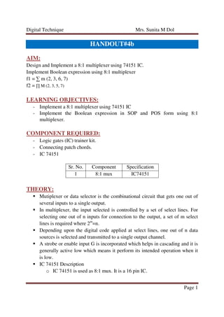
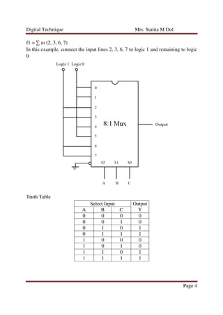
Digital Technique Mrs. Sunita M Dol
Page 1
HANDOUT#4b
AIM:
Design and Implement a 8:1 multiplexer using 74151 IC.
Implement Boolean expression using 8:1 multiplexer
f1 = ∑ m (2, 3, 6, 7)
f2 = ∏ M (2, 3, 5, 7)
LEARNING OBJECTIVES:
- Implement a 8:1 multiplexer using 74151 IC
- Implement the Boolean expression in SOP and POS form using 8:1
multiplexer.
COMPONENT REQUIRED:
- Logic gates (IC) trainer kit.
- Connecting patch chords.
- IC 74151
Sr. No. Component Specification
1 8:1 mux IC74151
THEORY:
Mutiplexer or data selector is the combinational circuit that gets one out of
several inputs to a single output.
In multiplexer, the input selected is controlled by a set of select lines. For
selecting one out of n inputs for connection to the output, a set of m select
lines is required where 2m
=n.
Depending upon the digital code applied at select lines, one out of n data
sources is selected and transmitted to a single output channel.
A strobe or enable input G is incorporated which helps in cascading and it is
generally active low which means it perform its intended operation when it
is low.
IC 74151 Description
o IC 74151 is used as 8:1 mux. It is a 16 pin IC.
Digital Technique Mrs. Sunita M Dol
Page 2
o Pin number 4, 3, 2, 1, 15, 14, 13, 12 acts as input signal from 0 to 7
respectively.
o Pin number 9, 10, 11 are the select inputs used to set an input.
o We get the output of this circuit at pin number 5. And its complement
on pin number 6.
o Pin number 7 acts as a strobe which is used for cascading purpose
otherwise it is connected to the ground.
o Pin number 16 is the power supply that is Vcc.
o The block diagram of IC 74151 is given in figure a and pin diagram of
IC 74151 is given in figure b.
Figure a: Block diagram
Digital Technique Mrs. Sunita M Dol
Page 3
Figure b: Pin diagram
Truth table:
Select Input Output
Y
S2 S1 S0
I0 0 0 0 0
I1 0 0 1 1
I2 0 1 0 2
I3 0 1 1 3
I4 1 0 0 4
I5 1 0 1 5
I6 1 1 0 6
I7 1 1 1 7
The design procedure is given below:
o Identify the decimal number corresponding to the each minterm in the
expression. The input lines corresponding to these numbers are to be
connected to logic 0 level.
o All other input lines are to be connected to logic 0 level.
o The inputs are to be applied to the select lines.
Given Logic function:
Digital Technique Mrs. Sunita M Dol
Page 4
f1 = ∑ m (2, 3, 6, 7)
In this example, connect the input lines 2, 3, 6, 7 to logic 1 and remaining to logic
0
Truth Table
Select Input Output
Y
A B C
0 0 0 0
0 0 1 0
0 1 0 1
0 1 1 1
1 0 0 0
1 0 1 0
1 1 0 1
1 1 1 1
Digital Technique Mrs. Sunita M Dol
Page 5
f2 = ∏ M (2, 3, 5, 7)
In this example, connect the input lines 2, 3, 5, 7 to logic 0 and remaining to logic
1
Truth Table
Select Input Output
Y
A B C
0 0 0 1
0 0 1 1
0 1 0 0
0 1 1 0
1 0 0 1
1 0 1 0
1 1 0 1
1 1 1 0
Digital Technique Mrs. Sunita M Dol
Page 6
PROCEDURE:
1. Check the components for their working.
2. Insert the appropriate IC into the IC base.
3. Make connections as shown in the circuit diagram.
4. Provide the input data via the input switches and observe the output on
output LEDs
5. Give various combinations of inputs and note down the output with help of
LED for all gate ICs one by one.
RESULT:
Thus we have implemented 8:1 multiplexer using 74151 IC and also implemented
Boolean expression using this multiplexer
f1 = ∑ m (2, 3, 6, 7)
f2 = ∏ M (2, 3, 5, 7)

Assignment#4b

  • 1.
    Digital Technique Mrs.Sunita M Dol Page 1 HANDOUT#4b AIM: Design and Implement a 8:1 multiplexer using 74151 IC. Implement Boolean expression using 8:1 multiplexer f1 = ∑ m (2, 3, 6, 7) f2 = ∏ M (2, 3, 5, 7) LEARNING OBJECTIVES: - Implement a 8:1 multiplexer using 74151 IC - Implement the Boolean expression in SOP and POS form using 8:1 multiplexer. COMPONENT REQUIRED: - Logic gates (IC) trainer kit. - Connecting patch chords. - IC 74151 Sr. No. Component Specification 1 8:1 mux IC74151 THEORY: Mutiplexer or data selector is the combinational circuit that gets one out of several inputs to a single output. In multiplexer, the input selected is controlled by a set of select lines. For selecting one out of n inputs for connection to the output, a set of m select lines is required where 2m =n. Depending upon the digital code applied at select lines, one out of n data sources is selected and transmitted to a single output channel. A strobe or enable input G is incorporated which helps in cascading and it is generally active low which means it perform its intended operation when it is low. IC 74151 Description o IC 74151 is used as 8:1 mux. It is a 16 pin IC.
  • 2.
    Digital Technique Mrs.Sunita M Dol Page 2 o Pin number 4, 3, 2, 1, 15, 14, 13, 12 acts as input signal from 0 to 7 respectively. o Pin number 9, 10, 11 are the select inputs used to set an input. o We get the output of this circuit at pin number 5. And its complement on pin number 6. o Pin number 7 acts as a strobe which is used for cascading purpose otherwise it is connected to the ground. o Pin number 16 is the power supply that is Vcc. o The block diagram of IC 74151 is given in figure a and pin diagram of IC 74151 is given in figure b. Figure a: Block diagram
  • 3.
    Digital Technique Mrs.Sunita M Dol Page 3 Figure b: Pin diagram Truth table: Select Input Output Y S2 S1 S0 I0 0 0 0 0 I1 0 0 1 1 I2 0 1 0 2 I3 0 1 1 3 I4 1 0 0 4 I5 1 0 1 5 I6 1 1 0 6 I7 1 1 1 7 The design procedure is given below: o Identify the decimal number corresponding to the each minterm in the expression. The input lines corresponding to these numbers are to be connected to logic 0 level. o All other input lines are to be connected to logic 0 level. o The inputs are to be applied to the select lines. Given Logic function:
  • 4.
    Digital Technique Mrs.Sunita M Dol Page 4 f1 = ∑ m (2, 3, 6, 7) In this example, connect the input lines 2, 3, 6, 7 to logic 1 and remaining to logic 0 Truth Table Select Input Output Y A B C 0 0 0 0 0 0 1 0 0 1 0 1 0 1 1 1 1 0 0 0 1 0 1 0 1 1 0 1 1 1 1 1
  • 5.
    Digital Technique Mrs.Sunita M Dol Page 5 f2 = ∏ M (2, 3, 5, 7) In this example, connect the input lines 2, 3, 5, 7 to logic 0 and remaining to logic 1 Truth Table Select Input Output Y A B C 0 0 0 1 0 0 1 1 0 1 0 0 0 1 1 0 1 0 0 1 1 0 1 0 1 1 0 1 1 1 1 0
  • 6.
    Digital Technique Mrs.Sunita M Dol Page 6 PROCEDURE: 1. Check the components for their working. 2. Insert the appropriate IC into the IC base. 3. Make connections as shown in the circuit diagram. 4. Provide the input data via the input switches and observe the output on output LEDs 5. Give various combinations of inputs and note down the output with help of LED for all gate ICs one by one. RESULT: Thus we have implemented 8:1 multiplexer using 74151 IC and also implemented Boolean expression using this multiplexer f1 = ∑ m (2, 3, 6, 7) f2 = ∏ M (2, 3, 5, 7)