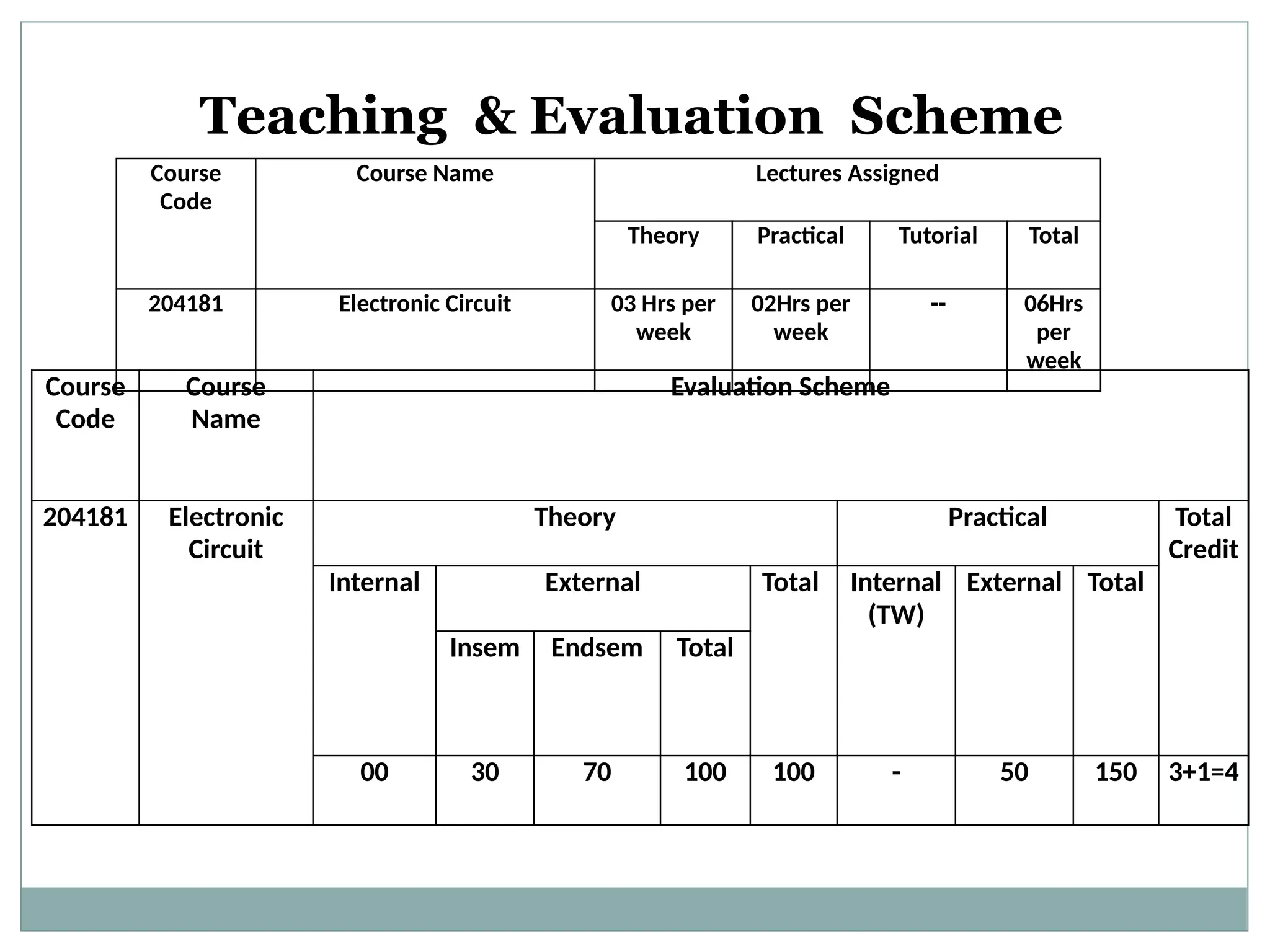
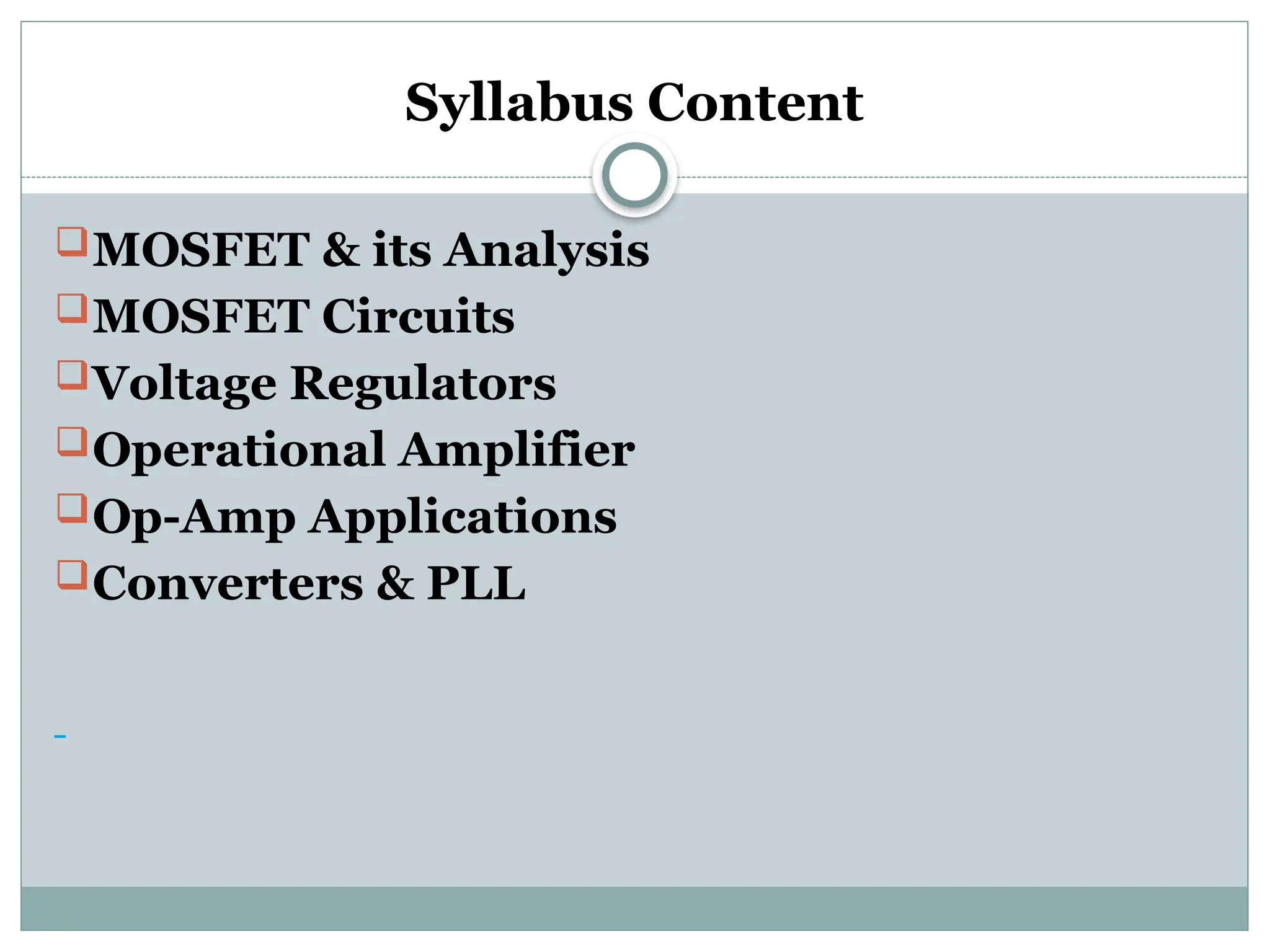
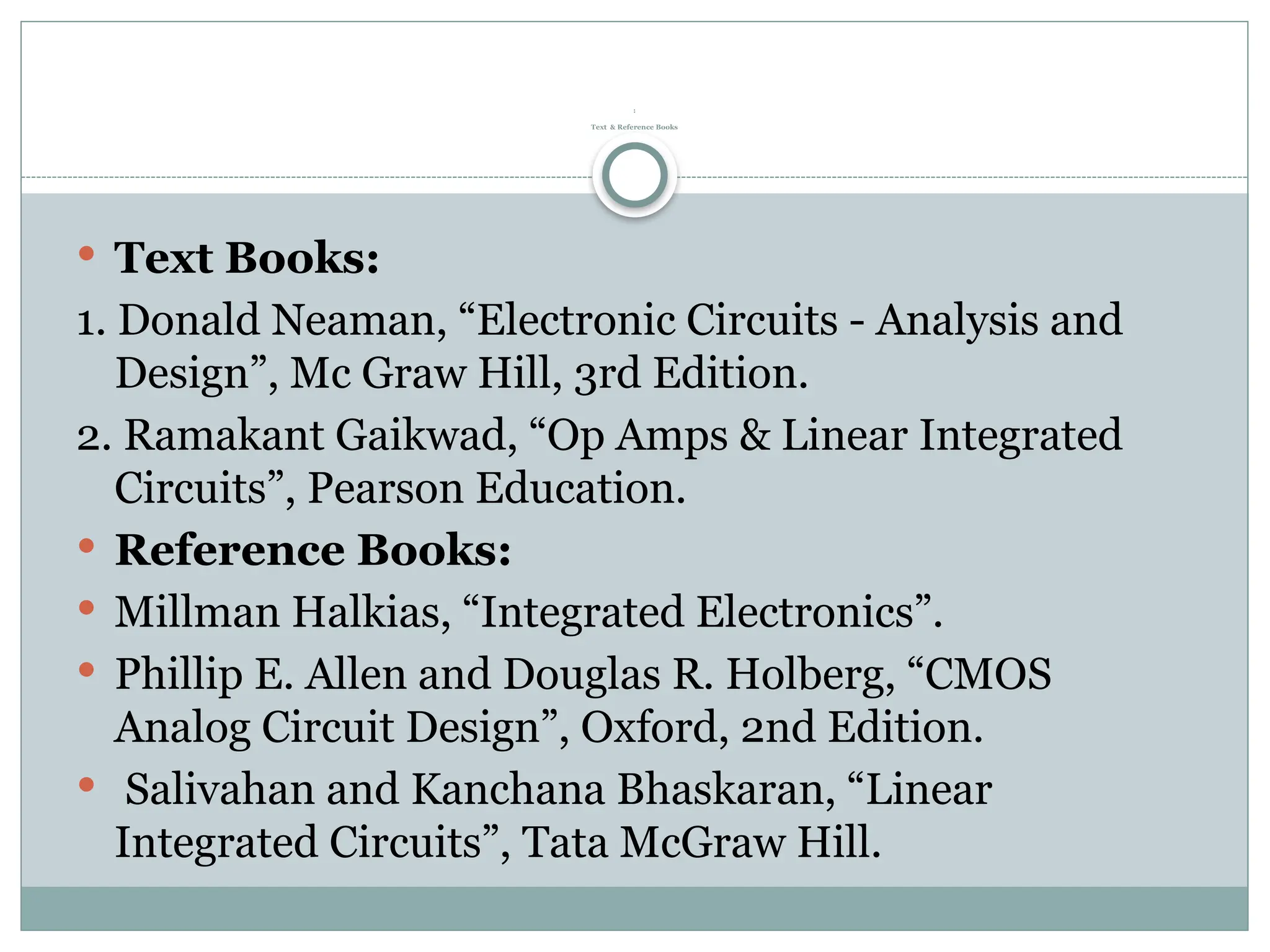
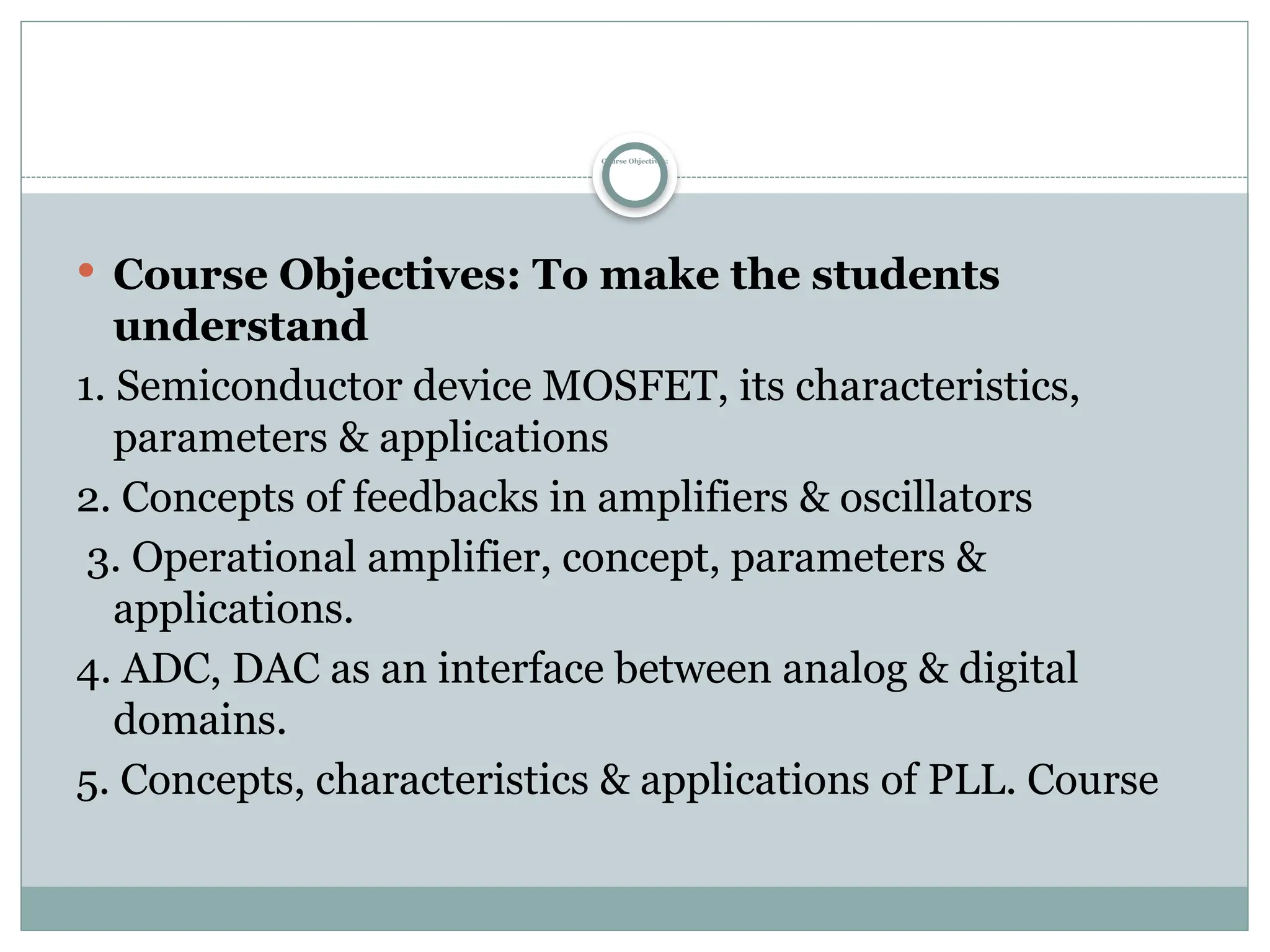
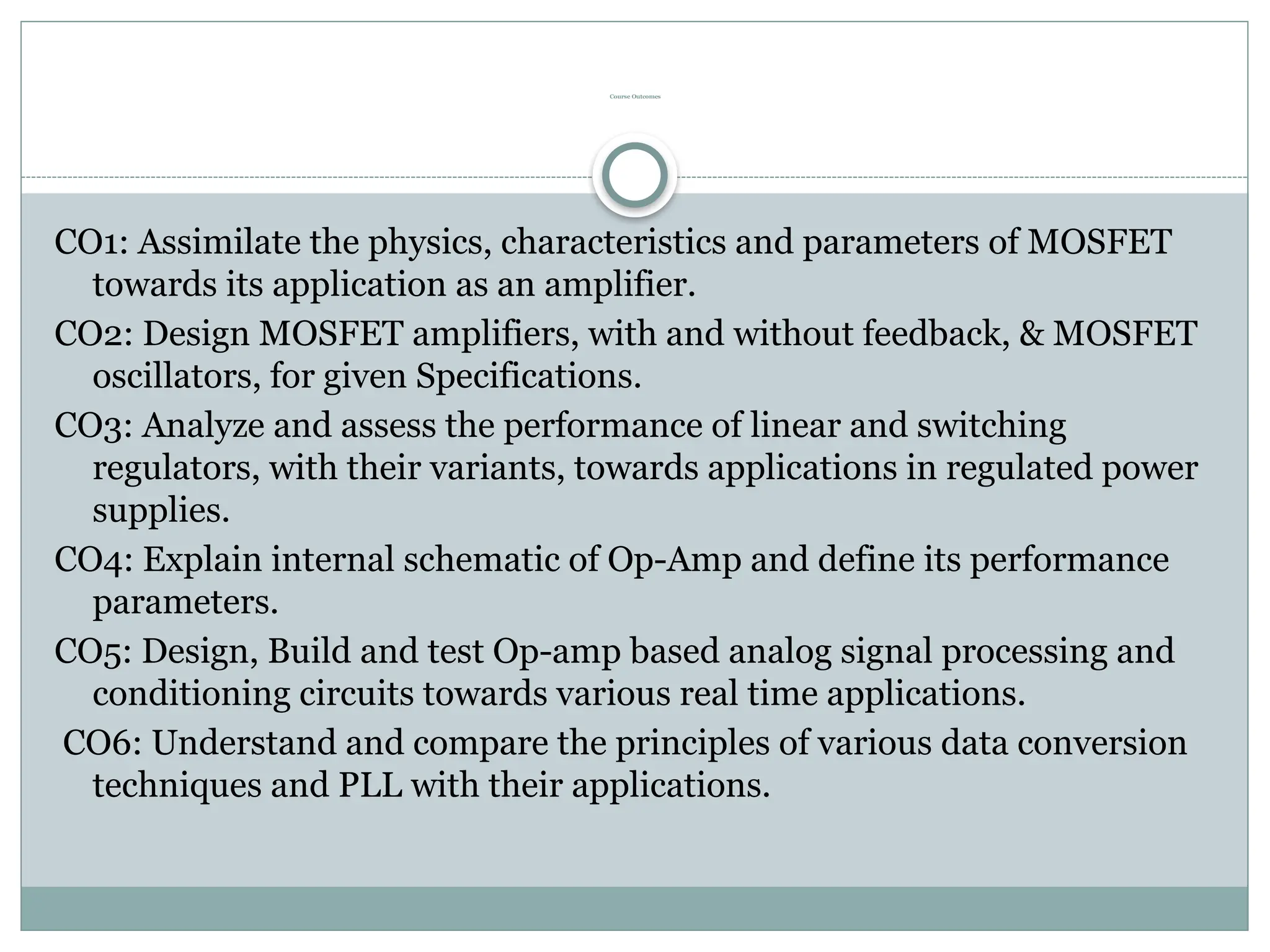
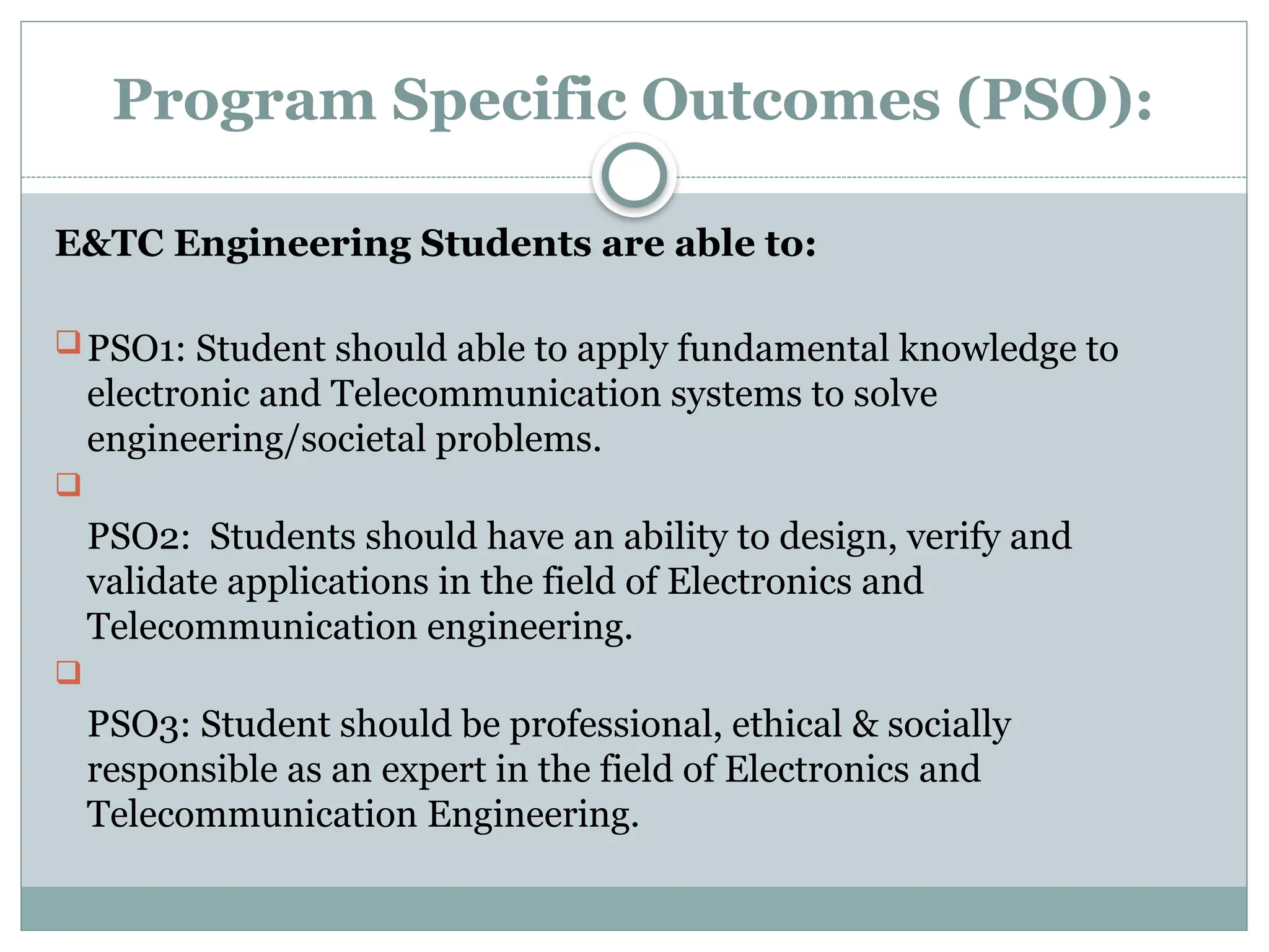
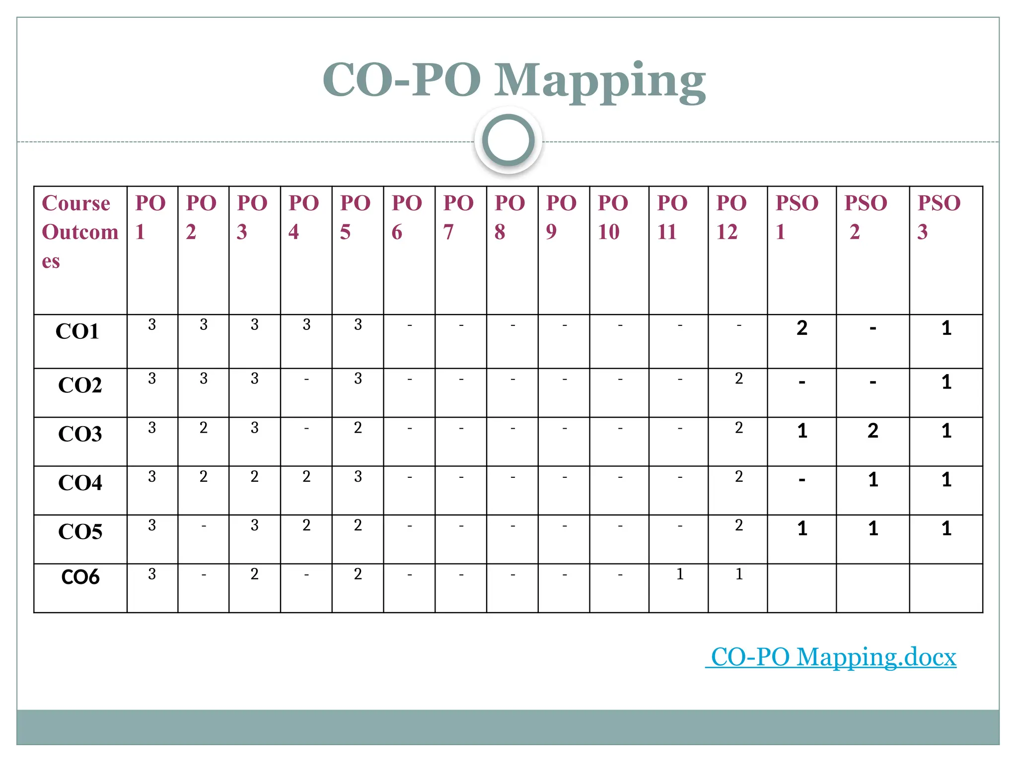
Faculty Orientation Programme
August 13th
2021
Welcome
Ms. A. A. Hatkar Prof.(Dr.)KTV Reddy
(HOD) (Principal)
Department of Electronics and Telecommunication
Engineering
Course: Electronic Circuits
Class : Second year
Subject Teacher : Ms. Trupti K. Wable
Syllabus
Teaching Scheme
Evaluation scheme
Course Objectives
Course Outcomes
Mapping of Course Outcomes
Overview
Teaching & Evaluation Scheme
Course
Code
Course Name Lectures Assigned
Theory Practical Tutorial Total
204181 Electronic Circuit 03 Hrs per
week
02Hrs per
week
-- 06Hrs
per
week
Course
Code
Course
Name
Evaluation Scheme
204181 Electronic
Circuit
Theory Practical Total
Credit
Internal External Total Internal
(TW)
External Total
Insem Endsem Total
00 30 70 100 100 - 50 150 3+1=4
Evaluation Guidelines
 Insem Examination [30 Marks]:
Paper pattern and marks distribution for In Semester Exam: As per
university guideline.
 End Semester Examination [ 70 Marks]:
Paper pattern and marks distribution for End Semester Exam: As per
university guideline.
 Term Work Evaluation[25Marks]:
 Average marks secured in all experiments: 10 Marks
 Average attendance in Theory & practical: 05 Marks
 Class test+ Preliminary Exam+ Assignments: 10 Marks
Syllabus Content
MOSFET & its Analysis
MOSFET Circuits
Voltage Regulators
Operational Amplifier
Op-Amp Applications
Converters & PLL
:
Text & Reference Books
 Text Books:
1. Donald Neaman, “Electronic Circuits - Analysis and
Design”, Mc Graw Hill, 3rd Edition.
2. Ramakant Gaikwad, “Op Amps & Linear Integrated
Circuits”, Pearson Education.
 Reference Books:
 Millman Halkias, “Integrated Electronics”.
 Phillip E. Allen and Douglas R. Holberg, “CMOS
Analog Circuit Design”, Oxford, 2nd Edition.
 Salivahan and Kanchana Bhaskaran, “Linear
Integrated Circuits”, Tata McGraw Hill.
Course Objectives:
 Course Objectives: To make the students
understand
1. Semiconductor device MOSFET, its characteristics,
parameters & applications
2. Concepts of feedbacks in amplifiers & oscillators
3. Operational amplifier, concept, parameters &
applications.
4. ADC, DAC as an interface between analog & digital
domains.
5. Concepts, characteristics & applications of PLL. Course
Course Outcomes
CO1: Assimilate the physics, characteristics and parameters of MOSFET
towards its application as an amplifier.
CO2: Design MOSFET amplifiers, with and without feedback, & MOSFET
oscillators, for given Specifications.
CO3: Analyze and assess the performance of linear and switching
regulators, with their variants, towards applications in regulated power
supplies.
CO4: Explain internal schematic of Op-Amp and define its performance
parameters.
CO5: Design, Build and test Op-amp based analog signal processing and
conditioning circuits towards various real time applications.
CO6: Understand and compare the principles of various data conversion
techniques and PLL with their applications.
Programme Outcomes (POs)
 PO1: Engineering Knowledge
 PO2: Problem Analysis
 PO3: Design & Development of Solutions
 PO4: Investigation of Complex Problem
 PO5: Modern Tools Usage
 PO6: Engineer and Society:
 PO7: Environment & Sustainability
 PO8: Ethics:
 PO9: Individual & Team work:
 PO10: Communication
 PO11: Project management & Finance:
 PO12: Lifelong Learning
Program Specific Outcomes (PSO):
E&TC Engineering Students are able to:
PSO1: Student should able to apply fundamental knowledge to
electronic and Telecommunication systems to solve
engineering/societal problems.

PSO2: Students should have an ability to design, verify and
validate applications in the field of Electronics and
Telecommunication engineering.

PSO3: Student should be professional, ethical & socially
responsible as an expert in the field of Electronics and
Telecommunication Engineering.
CO-PO Mapping
Course
Outcom
es
PO
1
PO
2
PO
3
PO
4
PO
5
PO
6
PO
7
PO
8
PO
9
PO
10
PO
11
PO
12
PSO
1
PSO
2
PSO
3
CO1 3 3 3 3 3 - - - - - - - 2 - 1
CO2 3 3 3 - 3 - - - - - - 2 - - 1
CO3 3 2 3 - 2 - - - - - - 2 1 2 1
CO4 3 2 2 2 3 - - - - - - 2 - 1 1
CO5 3 - 3 2 2 - - - - - - 2 1 1 1
CO6 3 - 2 - 2 - - - - - 1 1
CO-PO Mapping.docx
Additional Efforts to achieve remaining POs
i Class Room
Teaching
v Self Learning
Online Resources
ix Industry Visit
ii Tutorial vi Slides x Group Discussion
iii Remedial
Coaching
vii Simulations/
Demonstrations
xi Seminar/Oral
iv Lab Experiment viii Expert Lecture xii Case Study
Practical Course Outcomes
 Course Outcomes:
 After completion of course student will be able to
 Understand [L1: Knowledge] Interpret various biasing
techniques of MOSFET & JFET procedure to design feedback
amplifier
 Compute [L2: Comprehension] Comprehend the
fundamentals in explain the functionality of biasing & analysis
of MOSFET & JFET
 Evaluate [L2: Application] Analyze small signal model of
FET and MOSFET.
 Discuss [L3: Analysis] Analyze the concepts, design and
simulate the various models using MOSFET & JFET
CO-PO Mapping
Course
Outcom
es
PO
1
PO
2
PO
3
PO
4
PO
5
PO
6
PO
7
PO
8
PO
9
PO
10
PO
11
PO
12
PSO
1
PSO
2
PSO
3
CO1 2 1 1 2 - 1
CO2 2 2 1 2 - 1
CO3 2 2 1 2 1 1
CO4 2 - 2 2 1 1
Practical List
 Group A: [Any 4 to be performed]
1. To design, build single stage CS amplifier & verify dc
operating point.
2. To build & test single stage CS amplifier, plot frequency
response. Calculate Av, Ri, Ro & bandwidth.
3. To implement current series feedback amplifier &
measure Rif, Rof, Avf & bandwidth.
4. To implement MOSFET amplifier-based Wein bridge
oscillator.
5. To design & implement an adjustable voltage regulator
using three terminal voltage regulator IC.
 Group B: Compulsory
1. To measure following Op- amp parameters & compare with
specifications given in data sheet. [Any two Practical Op-Amp
can be used for comparison. e.g. LM741, OP07, LF351,
LF356, TI071, TI072]
 Input bias current
 Input offset current
 Input offset voltage
 Slew rate
 CMRR
2. To design, build & test integrator using Op-amp for given frequency
fa.
3. To design, build & test 2 or 3-bit R-2R ladder DAC.
4. To design, build & test Square and triangular waveform generator
using Op-Amp (LF351/6)
 Group C: [Any 2 to be performed]
1. To design, build & test Schmitt trigger using Op-
Amp (LF356, TI071)
2. To design, build & test three Op amp
Instrumentation amplifier for typical application.
3. To design, build & test 2-bit flash ADC.
Any Questions
Thank You

Introduction to electronics circuit & designs

  • 1.
    Faculty Orientation Programme August13th 2021 Welcome Ms. A. A. Hatkar Prof.(Dr.)KTV Reddy (HOD) (Principal) Department of Electronics and Telecommunication Engineering Course: Electronic Circuits Class : Second year Subject Teacher : Ms. Trupti K. Wable
  • 2.
    Syllabus Teaching Scheme Evaluation scheme CourseObjectives Course Outcomes Mapping of Course Outcomes Overview
  • 3.
    Teaching & EvaluationScheme Course Code Course Name Lectures Assigned Theory Practical Tutorial Total 204181 Electronic Circuit 03 Hrs per week 02Hrs per week -- 06Hrs per week Course Code Course Name Evaluation Scheme 204181 Electronic Circuit Theory Practical Total Credit Internal External Total Internal (TW) External Total Insem Endsem Total 00 30 70 100 100 - 50 150 3+1=4
  • 4.
    Evaluation Guidelines  InsemExamination [30 Marks]: Paper pattern and marks distribution for In Semester Exam: As per university guideline.  End Semester Examination [ 70 Marks]: Paper pattern and marks distribution for End Semester Exam: As per university guideline.  Term Work Evaluation[25Marks]:  Average marks secured in all experiments: 10 Marks  Average attendance in Theory & practical: 05 Marks  Class test+ Preliminary Exam+ Assignments: 10 Marks
  • 5.
    Syllabus Content MOSFET &its Analysis MOSFET Circuits Voltage Regulators Operational Amplifier Op-Amp Applications Converters & PLL
  • 6.
    : Text & ReferenceBooks  Text Books: 1. Donald Neaman, “Electronic Circuits - Analysis and Design”, Mc Graw Hill, 3rd Edition. 2. Ramakant Gaikwad, “Op Amps & Linear Integrated Circuits”, Pearson Education.  Reference Books:  Millman Halkias, “Integrated Electronics”.  Phillip E. Allen and Douglas R. Holberg, “CMOS Analog Circuit Design”, Oxford, 2nd Edition.  Salivahan and Kanchana Bhaskaran, “Linear Integrated Circuits”, Tata McGraw Hill.
  • 7.
    Course Objectives:  CourseObjectives: To make the students understand 1. Semiconductor device MOSFET, its characteristics, parameters & applications 2. Concepts of feedbacks in amplifiers & oscillators 3. Operational amplifier, concept, parameters & applications. 4. ADC, DAC as an interface between analog & digital domains. 5. Concepts, characteristics & applications of PLL. Course
  • 8.
    Course Outcomes CO1: Assimilatethe physics, characteristics and parameters of MOSFET towards its application as an amplifier. CO2: Design MOSFET amplifiers, with and without feedback, & MOSFET oscillators, for given Specifications. CO3: Analyze and assess the performance of linear and switching regulators, with their variants, towards applications in regulated power supplies. CO4: Explain internal schematic of Op-Amp and define its performance parameters. CO5: Design, Build and test Op-amp based analog signal processing and conditioning circuits towards various real time applications. CO6: Understand and compare the principles of various data conversion techniques and PLL with their applications.
  • 9.
    Programme Outcomes (POs) PO1: Engineering Knowledge  PO2: Problem Analysis  PO3: Design & Development of Solutions  PO4: Investigation of Complex Problem  PO5: Modern Tools Usage  PO6: Engineer and Society:  PO7: Environment & Sustainability  PO8: Ethics:  PO9: Individual & Team work:  PO10: Communication  PO11: Project management & Finance:  PO12: Lifelong Learning
  • 10.
    Program Specific Outcomes(PSO): E&TC Engineering Students are able to: PSO1: Student should able to apply fundamental knowledge to electronic and Telecommunication systems to solve engineering/societal problems.  PSO2: Students should have an ability to design, verify and validate applications in the field of Electronics and Telecommunication engineering.  PSO3: Student should be professional, ethical & socially responsible as an expert in the field of Electronics and Telecommunication Engineering.
  • 11.
    CO-PO Mapping Course Outcom es PO 1 PO 2 PO 3 PO 4 PO 5 PO 6 PO 7 PO 8 PO 9 PO 10 PO 11 PO 12 PSO 1 PSO 2 PSO 3 CO1 33 3 3 3 - - - - - - - 2 - 1 CO2 3 3 3 - 3 - - - - - - 2 - - 1 CO3 3 2 3 - 2 - - - - - - 2 1 2 1 CO4 3 2 2 2 3 - - - - - - 2 - 1 1 CO5 3 - 3 2 2 - - - - - - 2 1 1 1 CO6 3 - 2 - 2 - - - - - 1 1 CO-PO Mapping.docx
  • 12.
    Additional Efforts toachieve remaining POs i Class Room Teaching v Self Learning Online Resources ix Industry Visit ii Tutorial vi Slides x Group Discussion iii Remedial Coaching vii Simulations/ Demonstrations xi Seminar/Oral iv Lab Experiment viii Expert Lecture xii Case Study
  • 13.
    Practical Course Outcomes Course Outcomes:  After completion of course student will be able to  Understand [L1: Knowledge] Interpret various biasing techniques of MOSFET & JFET procedure to design feedback amplifier  Compute [L2: Comprehension] Comprehend the fundamentals in explain the functionality of biasing & analysis of MOSFET & JFET  Evaluate [L2: Application] Analyze small signal model of FET and MOSFET.  Discuss [L3: Analysis] Analyze the concepts, design and simulate the various models using MOSFET & JFET
  • 14.
  • 15.
    Practical List  GroupA: [Any 4 to be performed] 1. To design, build single stage CS amplifier & verify dc operating point. 2. To build & test single stage CS amplifier, plot frequency response. Calculate Av, Ri, Ro & bandwidth. 3. To implement current series feedback amplifier & measure Rif, Rof, Avf & bandwidth. 4. To implement MOSFET amplifier-based Wein bridge oscillator. 5. To design & implement an adjustable voltage regulator using three terminal voltage regulator IC.
  • 16.
     Group B:Compulsory 1. To measure following Op- amp parameters & compare with specifications given in data sheet. [Any two Practical Op-Amp can be used for comparison. e.g. LM741, OP07, LF351, LF356, TI071, TI072]  Input bias current  Input offset current  Input offset voltage  Slew rate  CMRR 2. To design, build & test integrator using Op-amp for given frequency fa. 3. To design, build & test 2 or 3-bit R-2R ladder DAC. 4. To design, build & test Square and triangular waveform generator using Op-Amp (LF351/6)
  • 17.
     Group C:[Any 2 to be performed] 1. To design, build & test Schmitt trigger using Op- Amp (LF356, TI071) 2. To design, build & test three Op amp Instrumentation amplifier for typical application. 3. To design, build & test 2-bit flash ADC.
  • 18.