
Recommended
Recommended
More Related Content
Similar to Analog VLSI CIrcuits_beforeMID_merged.pdf
Similar to Analog VLSI CIrcuits_beforeMID_merged.pdf (20)
Recently uploaded
Recently uploaded (20)
Analog VLSI CIrcuits_beforeMID_merged.pdf
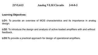
- 1. Learning Objectives: LO1: To provide an overview of MOS characteristics and its importance in analog design. LO2: To introduce the design and analysis of active loaded amplifiers with and without feedback. LO3:To provide a practical approach for design of operational amplifiers.
- 2. Course Outcomes: CO1: Ability to understand MOS characteristics and the design of current sources. CO2: Ability to apply techniques to design actively loaded amplifiers with and without feedback. CO3: Ability to design and analyze operational amplifiers, comparators and oscillators. CO4: Ability to evaluate amplifier characteristics from top-level specifications using circuit simulators.
- 3. Skills Acquired: Provides a platform to design CMOS amplifiers with the help of industry standard tools.
- 4. Unit 1: MOS Large-Signal and Small-Signal Equivalents, Biasing, High-Frequency Modeling, Short Channel, Subthreshold Operation, Leakage Current, MOS Diodes, Active Resistors, Capacitors, Current Sink and Source, Cascode Current Mirrors, Gain-Boosting, Current and Voltage References, Supply Independent Biasing, Sensitivity. Unit 2: MOS Inverters, Active Load, Current Source Load, Push-Pull Load, Small Signal Gain, Frequency Response, Miller Effect-3-dB Frequency Determination, Single-Stage MOS Amplifiers, Common Gate - Common Drain, Cascode, Differential Amplifiers, Active Loaded Differential Pair, Feedback Amplifiers, Negative Feedback, Loop Gain, Oscillators, Comparators. Unit 3: Two-Stage CMOS Op-Amp Design, Gain and Frequency Response, Stability and Compensation in CMOS Op-Amps, Miller Compensated Op-Amp, Lead-Lag Compensation, Case Study of ADA4528: A Zero Drift and Ultralow Noise Op-Amp Course Contents
- 5. 1. B. Razavi, Design of Analog CMOS Integrated Circuits, Tata McGraw Hill, 2002, Reprint 2015. 2. P. E. Allen and D. R. Holberg, CMOS Analog Circuit Design, Third Edition, Oxford Press, 2011. 3. P. R. Gray, P. J. Hurst, S. H. Levis and R. G. Meyer, Analysis and Design of Analog Integrated Circuits, Fifth Edition, Wiley Student Edition, 2009. 4. A S. Sedra, K. C. Smith and A. N. Chandorkar, Microelectronic Circuits -Theory and Applications, Seventh Edition, Oxford University Press, 2017. References
- 6. Assessment Interna/ External Maximum Marks Weightage Quiz-1 Internal 10 7.5 Quiz-2 10 7.5 Mid-Term Examination 50 30 Quiz-3 10 7.5 Quiz-4 10 7.5 End Semester Examination External 100 40 Total 100 Evaluation Pattern: (60:40)
- 7. Analog VLSI design refers to the process of designing and fabricating ICs that primarily involve analog electronic components and circuits on a single semiconductor chip. Analog circuits deal with continuous signals, such as voltages and currents, as opposed to digital circuits that work with discrete values (0s and 1s). Analog VLSI Design
- 8. Analog VLSI design involves creating complex systems on a chip that can perform various functions, such as amplification, filtering, signal conditioning, voltage regulation, and more. Some common examples of analog VLSI circuits include operational amplifiers, voltage regulators, analog-to-digital converters (ADCs), digital- to-analog converters (DACs), and radio-frequency (RF) circuits. Analog VLSI Design Digital VLSI is a more mature field than analog VLSI. This is because digital circuits are easier to design and fabricate. Digital circuits also have a wider range of commercial applications.
- 9. Designing analog VLSI circuits can be challenging due to the inherent complexities of dealing with real-world phenomena like noise, signal distortion, temperature effects, and process variations. Designers need a deep understanding of semiconductor physics, analog circuit theory, device modeling, and fabrication processes. Analog VLSI design plays a crucial role in various applications, including communications, sensor interfaces, audio and video processing, medical electronics, and more. It requires a combination of creativity, engineering expertise, and a solid foundation in analog electronics to successfully design and produce functional analog VLSI circuits. Analog VLSI Design
- 10. Analog VLSI is a more challenging field to design than digital VLSI. This is because analog circuits are more sensitive to noise and power consumption. Analog circuits also require a more thorough understanding of semiconductor physics and device modeling. Analog vs. Digital VLSI Design
- 11. Voltage and Current Amplifier
- 12. Power Amplifier
- 15. Power: Passive Network If ideal transformer is considered If a passive network is considered This will NOT guarantee either voltage or current amplification
- 16. Maximum Power Delivered If power and voltage amplification is required, then RL > 4RS
- 17. Maintain Constant Output Voltage Maintain the output volage regardless of RL Output voltage regulation
- 18. Variable Load Resistance NOT possible by one equation. Because resistance RL is varying
- 19. Maintain Constant Output Voltage Keping the output voltage (VO) same and get the power amplification (Pout > Pin) Voltage Regulation
- 20. Example: Variable RL It does NOT satisfy for a range of RL It is for fixed value of RL
- 21. Example: Loading of the Network by RL
- 22. Example: Loading of the Network by RL
- 24. Example: Loading of the Network by RL
- 25. Example: Loading of the Network by RL
- 26. Example: Range of Current for varying RL
- 27. Example: Controlling VO by adjusting R1
- 28. Negative Feedback Instead of using fixed R use variable R → R1 Resistive ratio will be insensitive to changes in RL This helps in analysing whether a given network is able to drive the connected load OR not.
- 29. Current and Voltage Sources For an ideal voltage source if the terminals are shorted, the current ISC will be Ꝏ
- 30. Practical Current and Voltage Sources Source resistance RS = 0. This is practically NOT possible There exists a nonzero small value of RS associated with voltage source
- 31. Good voltage or current source depends on the relation between RS and RL Consider RS = 100Ω Current Source Voltage Source Practical Current and Voltage Sources
- 32. Motivations
- 33. Requirement of a bias voltage for power amplification Bias volage VDC
- 34. Requirement of additional supply for power amplification
- 35. Superposition of Signals: Linear Systems It describes how signals interact when they are combined.
- 36. Superposition of Signals: Linear Systems N N
- 37. Power Amplification: LTI Systems
- 38. LTI Systems: Concept of Frequency Shift
- 39. Power Amplification: Non-Linear Systems
- 40. Consequence of Non - Linearity
- 41. Linearization of the Non-linear Element Resistor (RL) Non-Linear Element Relation between current and voltage
- 42. Current and Voltage Relation Voltage Source Non-Linear Element I-V Relation
- 43. Variation in the input Vi Current IN Incremental Current ∆IN Change in Source Voltage
- 44. Linear Relationship Required Taylor Series Applied Non-Linear Device
- 45. Linear Relationship Established Neglect the higher order terms
- 46. Incremental Quantity Approximated Relationship of incremental quantities
- 48. Non-Linear Element: Final Remark
- 49. Incremental Current and Voltage Equivalents
- 50. Small Signal Model Small Signal Model
- 51. Linearized Models of Common Electrical Elements
- 53. Example: Diode Equation Apply KVL to the Circuit Diode Equation Quiescent point assumed to be 0.7V
- 54. Example: Small Signal (Diode) Incremental Voltage is 0.1V Original Diode Circuit Linearized Circuit Diode equation
- 55. Example: Small Signal (Diode) Linearized Resistance of Diode Linearized Diode Circuit Quiescent Voltage + Incremental Quiescent Current + Incremental
- 56. Small Signal Analysis of Forward Bias Diode Neglect the higher order terms Based on the condition Final condition of small signal
- 57. A two-port network is an electrical network with two pairs of terminals to connect to external circuits. Two terminals constitute a port if the currents applied to them satisfy the essential requirement known as the port condition: the current entering one terminal must equal the current emerging from the other terminal on the same port. The ports constitute interfaces where the network connects to other networks, the points where signals are applied, or outputs are taken. Two - Port Network
- 58. A 2-port network in electronics is a fundamental concept used to analyze and describe the behavior of electrical circuits or systems with two input terminals and two output terminals. These networks are used to model and understand the interaction of electrical signals as they pass through various components, such as amplifiers, filters, transformers, and transmission lines. Two - Port Network The voltage at port 1 (V1) The current at port 1 (I1) The voltage at port 2 (V2) The current at port 2 (I2)
- 59. Input Ports: These are the two terminals where electrical signals are applied as inputs to the network. The signals entering the network can be voltage or current, depending on the specific application. Output Ports: These are the two terminals from which the network delivers its output signals. Like the input, the output signals can also be voltage or current. Characteristics and Parameters of 2-port networks
- 60. Transfer Parameters (T-parameters): Another set of parameters used to describe 2- port networks is the transfer parameters (T-parameters). These parameters relate input to output in terms of voltage and current, providing insight into how the network transforms signals. Hybrid Parameters (H-parameters): Hybrid parameters describe the network in terms of input current and output voltage (or vice versa). They are particularly useful for analyzing transistors and other semiconductor devices. Impedance Parameters (Z-parameters): Impedance parameters describe the network in terms of input and output impedance, which is valuable for matching networks and impedance transformations. Admittance Parameters (Y-parameters): Admittance parameters describe the network in terms of input and output admittance, which is also useful for certain types of analysis. Characteristics and Parameters of 2-port networks
- 61. 2-port networks are used extensively in Electronics, Telecommunications, and RF (radio frequency) engineering to analyze, design, and optimize circuits and systems. They allow engineers to understand how components interact with signals and to predict the overall performance of complex systems. These networks are essential tools in fields such as microwave engineering, antenna design, and amplifier design, among others. Applications: Two-port Networks
- 62. 3-Step Process for Converting Non-linear to Linear Step – 1: Step – 2: Step – 3: Note the notation also It is used to figure out the total current and voltage This kind of notations are inconvenient in representation
- 63. Two-Port Non-linear Network Representation To find out what is the relation between currents I1 and I2 What is the gain of the system? 2-PORT Network representation
- 64. Two-Port Non-linear Network Current IDC is dropped from the argument as it will NOT change the argument Quiescent Network For neglecting Incremental current Quiescent Condition
- 65. Two-Port Non-linear Network Y11 Y12 Y21 Y22 All the derivatives (Y) are constants
- 68. Summary: Two-Port Non-Linear Network
- 69. Relation: Input Voltage and Output Current
- 70. Relation: Input Voltage and Output Current
- 71. Relation: Input Voltage and Output Current
- 72. Relation: Input Voltage and Output Current
- 73. Incremental Gain of a Non-Linear Two Port Network
- 74. Incremental Gain of a Non-Linear Two Port Network
- 75. Representation of a Non-Linear Two-Port Network Based on the assumed condition
- 76. I-V Characteristics of the Non-Linear Two Port Network
- 77. Desirable I-V Characteristics of the Non-Linear Two Port Network
- 78. Revision of the Non-Linear Two Port Network
- 79. Desirable I-V Characteristics of the Non-Linear Two Port Network for Power Amplification For Reference
- 80. Desirable I-V Characteristics of the Non-Linear Two Port Network for Power Amplification
- 81. Desirable I-V Characteristics of the Non-Linear Two Port Network for Power Amplification
- 82. Desirable I-V Characteristics of the Non-Linear Two Port Network for Power Amplification
- 83. MOSFET
- 84. MOSFET
- 85. MOSFET
- 86. MOSFET
- 87. MOSFET
- 88. I-V Characteristics of the MOSFET
- 89. I-V Characteristics of the MOSFET
- 90. I-V Characteristics of the MOSFET
- 91. I-V Characteristics of the MOSFET
- 92. I-V Characteristics of the MOSFET
- 93. I-V Characteristics of the MOSFET
- 94. I-V Characteristics of the MOSFET
- 95. I-V Characteristics of the MOSFET
- 96. I-V Characteristics of the MOSFET (Common Source)
- 97. I-V Characteristics of the MOSFET
- 98. I-V Characteristics of the MOSFET
- 99. I-V Characteristics of the MOSFET
- 100. I-V Characteristics of the MOSFET