Download as PDF, PPTX


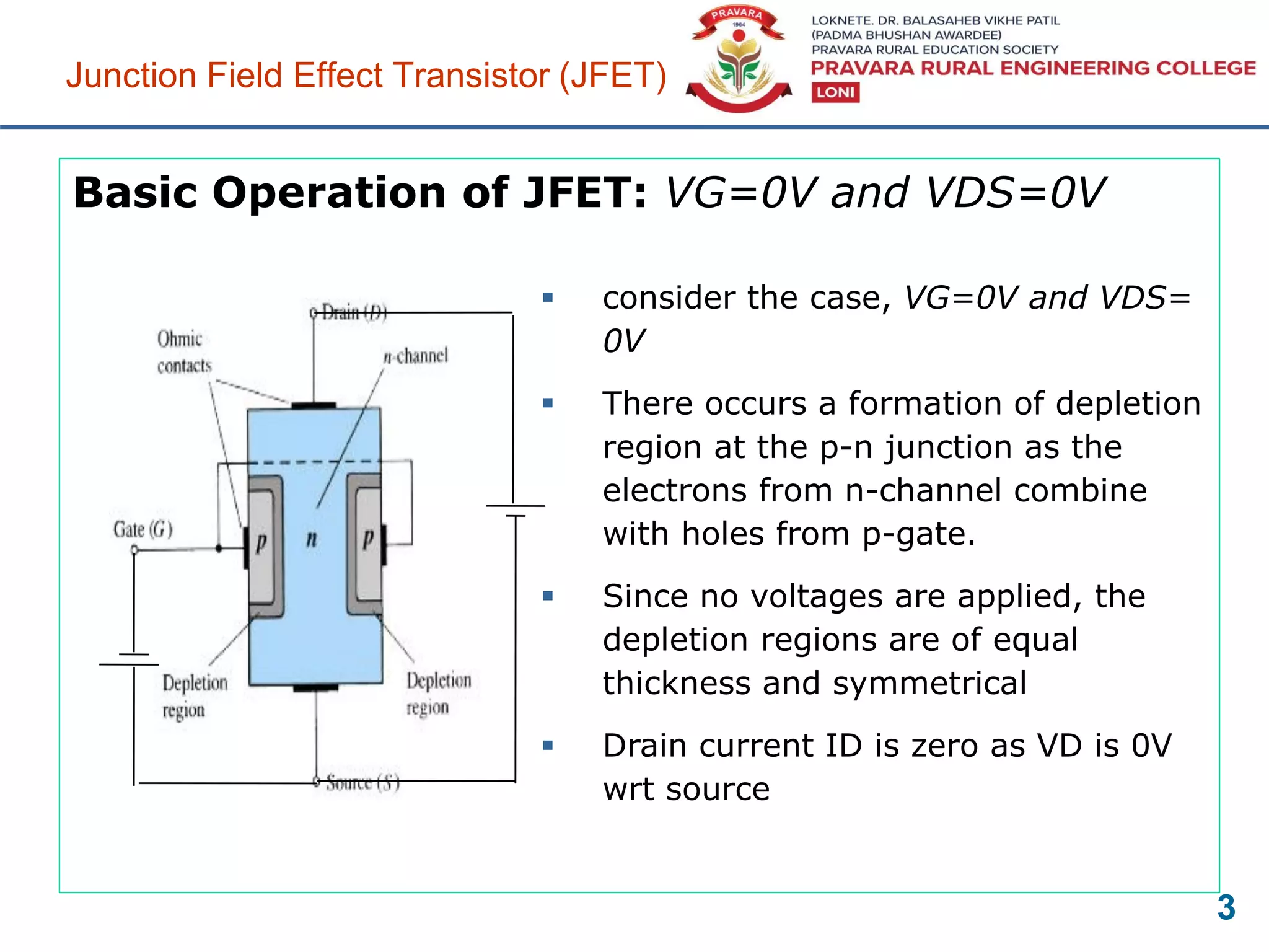
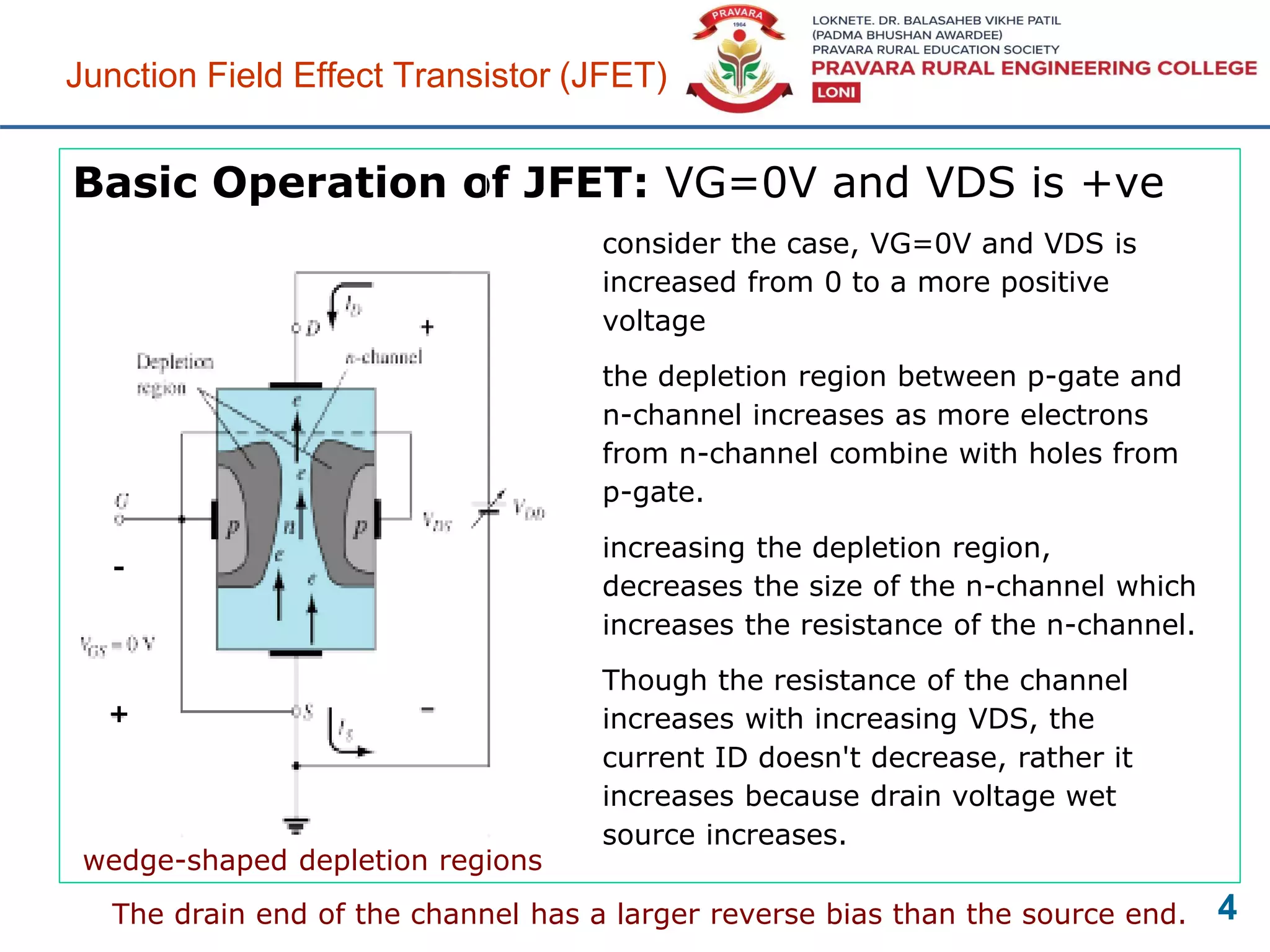

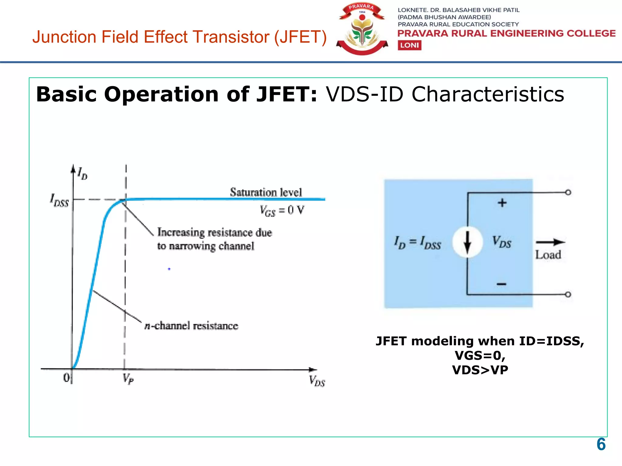
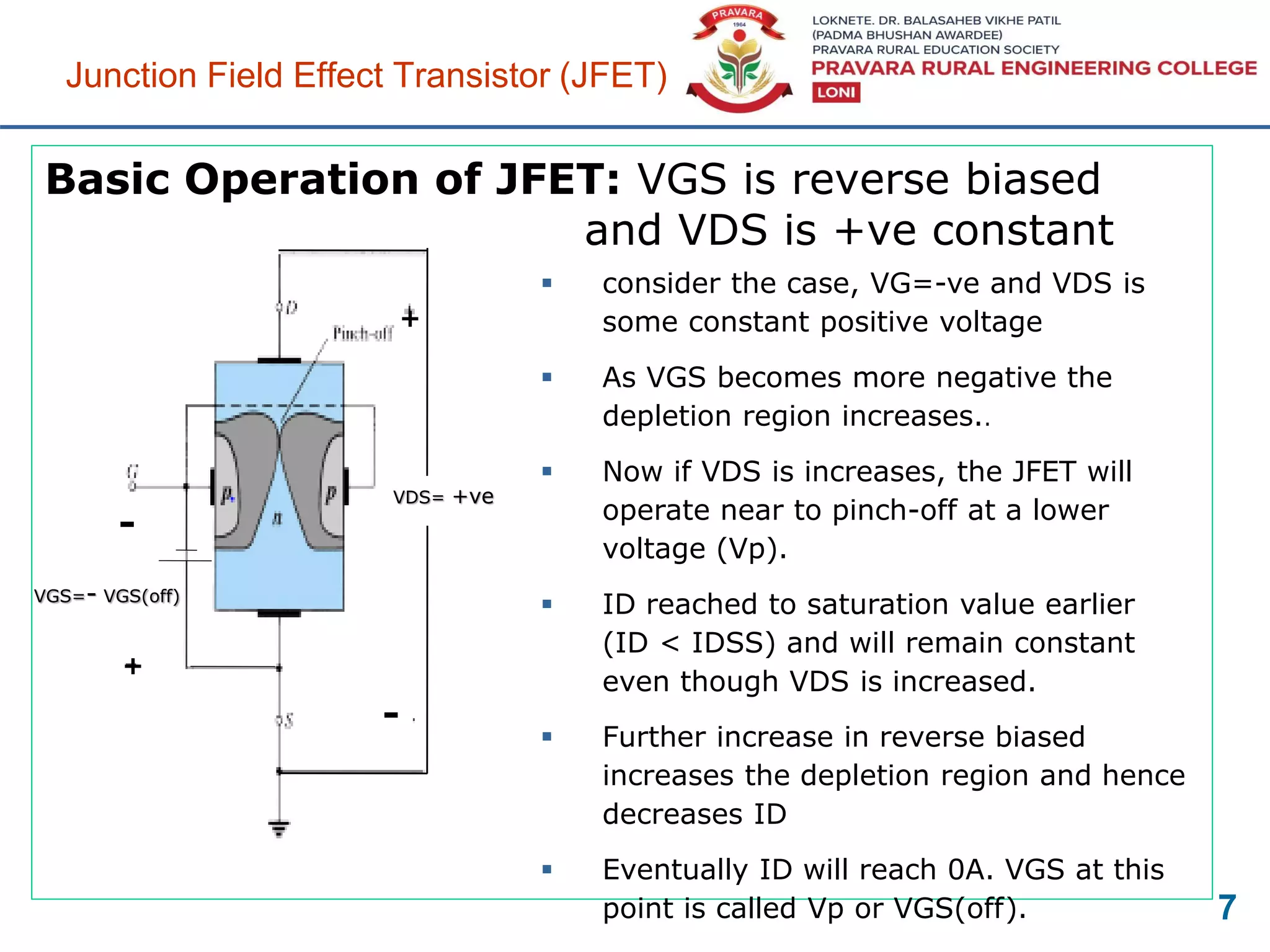
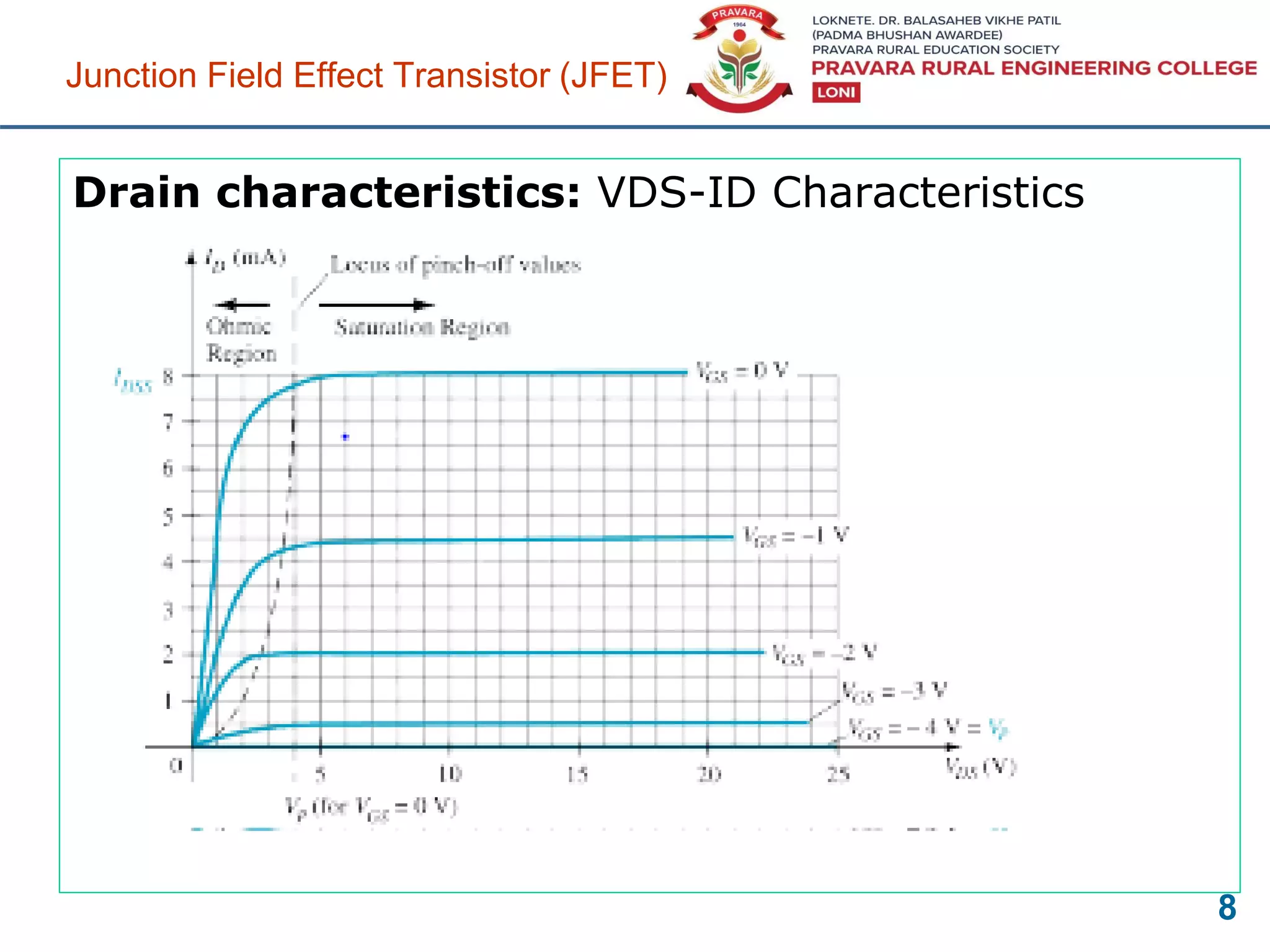


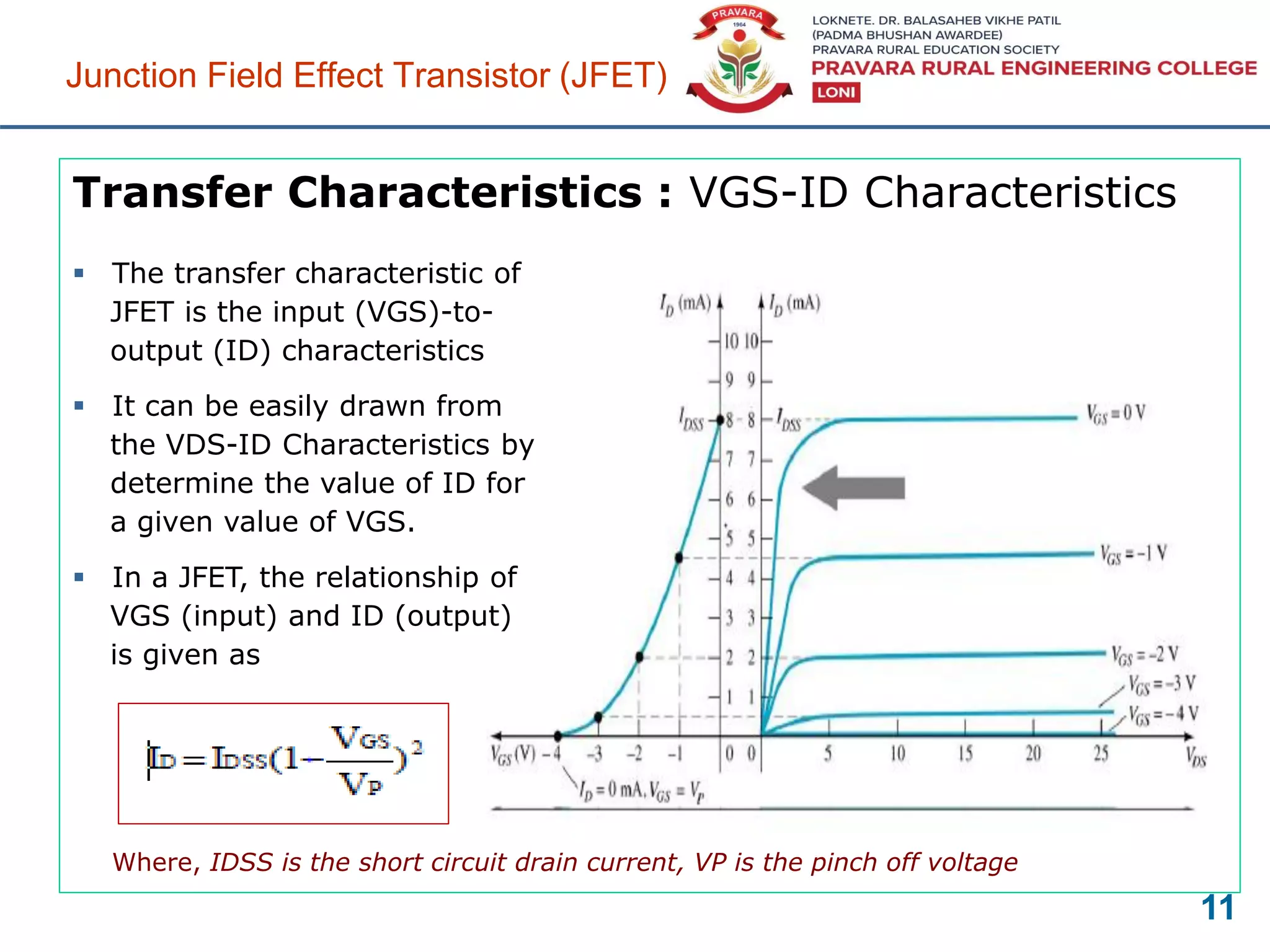
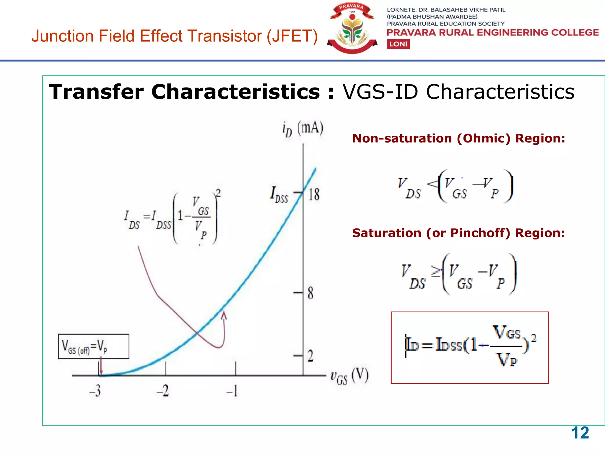


This document discusses the drain and transfer characteristics of junction field effect transistors (JFETs). It describes how applying different gate-source (VGS) and drain-source (VDS) voltages affects the depletion region and current flow (ID) in the device. Key points covered include: - At VGS=0 and low VDS, ID increases linearly as depletion regions are symmetrical - As VDS increases, depletion regions become asymmetrical, reducing the channel and increasing resistance but still allowing ID to rise - At pinch-off, the depletion regions almost close the channel, capping ID at its saturation value (IDSS) - Varying VGS controls the pinch-off voltage and ID