Presentation
of
Curriculum of Introductionto Electronics Engineering (IEE)
Department of Electronics and Communication Engineering
C.V. Raman Global University
Bhubaneswar - 752 054 (Odisha)
Dr. Virender Singh, Assistant Professor
2.
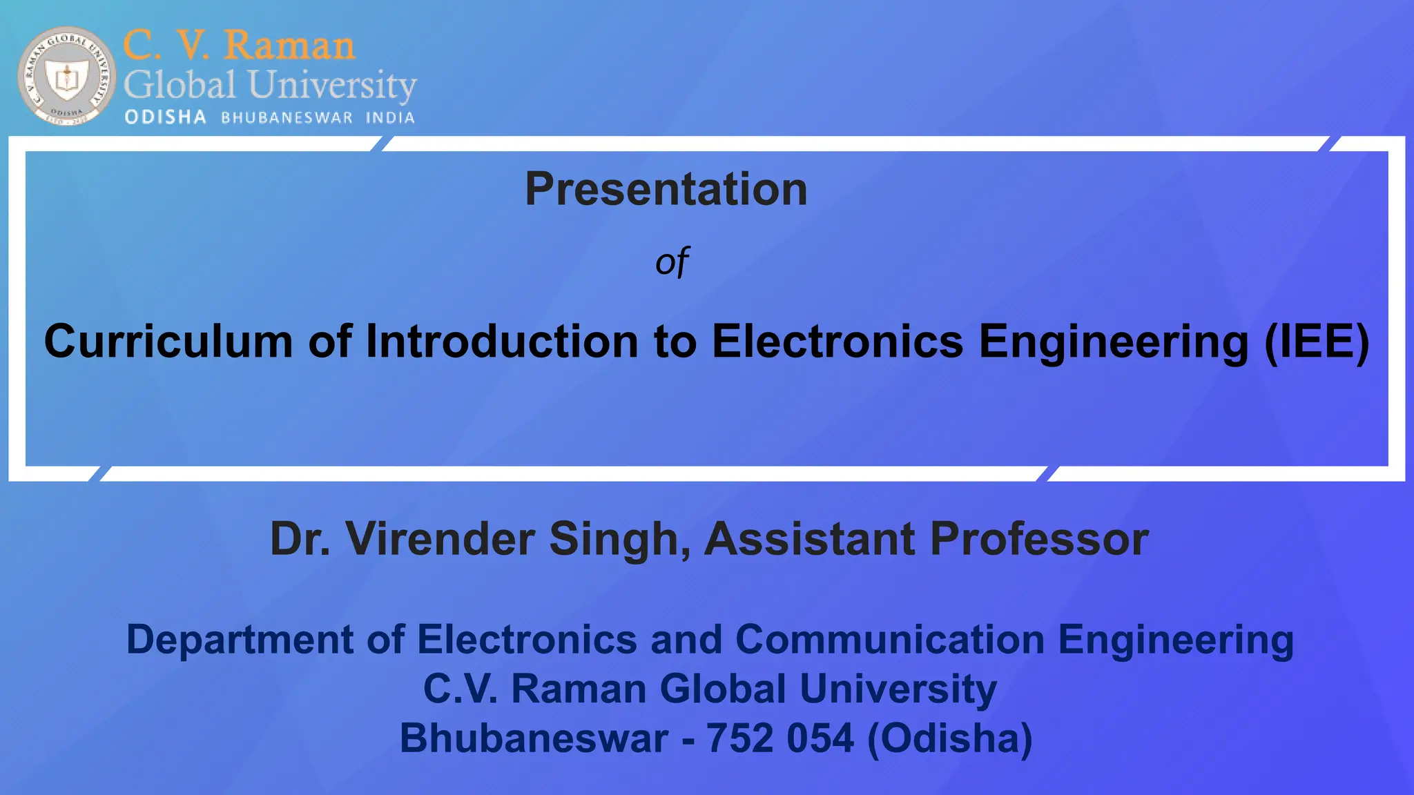
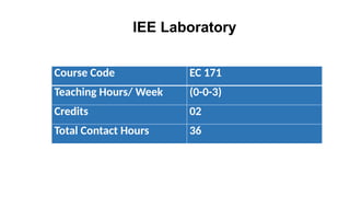
Course Code EC101
Teaching Hours/ Week (3-0-1-0)
Credits 03
Total Contact Hours 42
IEE Theory
C. V. Raman Global University, Odisha
3.
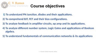
1) To understandPN Junction, diodes and their applications.
2) To comprehend BJT, FET and their bias configurations.
3) To analyze feedback in amplifier circuits, op amp and its applications.
4) To analyze different number system, Logic Gates and applications of Boolean
algebra.
5) To understand fundamentals of communication networks & its applications
Course objectives
C. V. Raman Global University, Odisha
4.
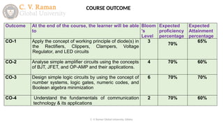
Outcome At theend of the course, the learner will be able
to
Bloom
’s
Level
Expected
proficiency
percentage
Expected
Attainment
percentage
CO-1 Apply the concept of working principle of diode(s) in
the Rectifiers, Clippers, Clampers, Voltage
Regulator, and LED circuits
3
70%
65%
CO-2 Analyse simple amplifier circuits using the concepts
of BJT, JFET, and OP-AMP and their applications.
4 70% 60%
CO-3 Design simple logic circuits by using the concept of
number systems, logic gates, numeric codes, and
Boolean algebra minimization
6 70% 70%
CO-4 Understand the fundamentals of communication
technology & its applications
2 70% 60%
COURSE OUTCOME
C. V. Raman Global University, Odisha
5.
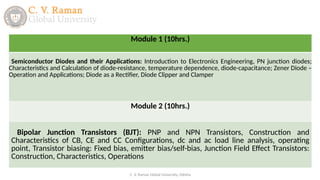
Module 1 (10hrs.)
SemiconductorDiodes and their Applications: Introduction to Electronics Engineering, PN junction diodes;
Characteristics and Calculation of diode-resistance, temperature dependence, diode-capacitance; Zener Diode –
Operation and Applications; Diode as a Rectifier, Diode Clipper and Clamper
Module 2 (10hrs.)
Bipolar Junction Transistors (BJT): PNP and NPN Transistors, Construction and
Characteristics of CB, CE and CC Configurations, dc and ac load line analysis, operating
point, Transistor biasing: Fixed bias, emitter bias/self-bias, Junction Field Effect Transistors:
Construction, Characteristics, Operations
C. V. Raman Global University, Odisha
6.
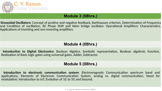
Module 3 (08hrs.)
SinusoidalOscillators: Concept of positive and negative feedback, Barkhausen criterion, Determination of Frequency
and Condition of oscillation, RC Phase Shift and Wein bridge oscillator. Operational Amplifiers: Characteristics,
Applications of Inverting and non-inverting amplifiers.
Module 4 (08hrs.)
Introduction to Digital Electronics: Boolean Algebra, Symbolic representation, Boolean algebraic function,
Realization of Basic logic gates using universal gates, Adder, Subtractor.
Module 5 (08hrs.)
Introduction to electronic communication system: Electromagnetic Communication spectrum band and
applications, Elements of Electronic Communication System, analog vs. digital communication, Need for
modulation; Introduction to IoT, Evolution of 1G to 5G and beyond.
C. V. Raman Global University, Odisha
7.
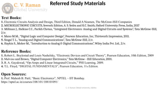
Text Books:
1. ElectronicCircuits Analysis and Design, Third Edition, Donald A Neamen, The McGraw-Hill Companies
2. MICROELECTRONIC CIRCUITS, Seventh Edition, A. S. Sedra and K.C. Smith, Oxford University Press, India, 2017
3. Millman J., Halkias C.C., Parikh Chetan, “Integrated Electronics: Analog and Digital Circuits and Systems”, Tata McGraw-Hill,
2/e.
4. Mano M.M., “Digital Logic and Computer Design”, Pearson Education, Inc, Thirteenth Impression, 2011.
5. Singal T. L., “Analog and Digital Communications”, Tata McGraw-Hill, 2/e.
6. Haykin S., Moher M., “Introduction to Analog & Digital Communications”, Wiley India Pvt. Ltd., 2/e.
Reference Books:
1. Robert L. Boylestad and Louis Nashelsky, “Electronic Devices and Circuit Theory”, Pearson Education, 10th Edition, 2009
2. Malvino and Brown, “Digital Computer Electronics,” Tata McGraw - Hill Education, 2001.
3. R. A. Gayakwad, “Op-Amps and Linear Integrated Circuits,” PHI Learning, 2009.
4. T.L. Floyd, “DIGITAL FUNDAMENTALS”, Pearson Education, 11th Edition.
Open Sources:
1. Prof. Mahesh B. Patil, “Basic Electronics”, NPTEL – IIT Bombay.
https://nptel.ac.in/courses/108/101/108101091/
Referred Study Materials
C. V. Raman Global University, Odisha
8.
Semiconductors
C. V. RamanGlobal University, Odisha
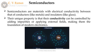
Semiconductors are materials with electrical conductivity between
that of conductors (like metals) and insulators (like glass).
Their unique property is that their conductivity can be controlled by
adding impurities or applying external fields, making them the
foundation of modern electronics.
9.
Semiconductors
C. V. RamanGlobal University, Odisha
Intrinsic Semiconductors:Pure Form: Intrinsic semiconductors are
pure semiconducting materials without any significant impurities.
Silicon (Si) and germanium (Ge) are common
examples.Conductivity: In an intrinsic semiconductor, the number
of electrons in the conduction band (where they can move freely)
equals the number of holes (empty states in the valence band where
an electron could exist).
Both electrons and holes contribute to electrical conduction.
Temperature Dependence: At absolute zero, intrinsic
semiconductors act as insulators. As temperature increases, more
electrons gain enough energy to jump from the valence band to the
conduction band, increasing conductivity.
10.
Semiconductors
C. V. RamanGlobal University, Odisha
Extrinsic Semiconductors:
Doped Semiconductors: Extrinsic semiconductors are created by adding
specific impurities, called dopants, to an intrinsic semiconductor to enhance its
conductivity.
Types of Extrinsic Semiconductors:
n-type: Doping with elements having more valence electrons than the
semiconductor (e.g., adding phosphorus to silicon) creates an excess of
electrons, which are the primary charge carriers.
p-type: Doping with elements having fewer valence electrons (e.g., adding
boron to silicon) creates more holes, which act as the primary charge
carriers.
Functionality: The controlled addition of dopants allows precise control over
the electrical properties of semiconductors, making them essential in devices
like diodes, transistors, and integrated circuits.
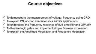
Course objectives
Todemonstrate the measurement of voltage, frequency using CRO
To explain PN junction characteristics and its applications.
To understand the frequency response of BJT amplifier and OPAMP.
To Realize logic gates and implement simple Boolean expression.
To explain the Amplitude Modulation and Frequency Modulation
14.
Experiment1 Measurements usingCRO to understand the Measurement of voltage, time
period and frequency of different signals on CRO and measurement
Experiment2 Study on PN Junction Characteristics to determine the forward bias V-I
characteristics of PN junction diode and finding its forward cut-in & reverse
breakdown voltage.
Experiment3 Design a basic voltage regulator circuit using Zener diode & determine the
reverse bias V-I characteristics of Zener diode and finding its reverse
breakdown voltage.
Experiment4 Analysis of the basic operation principle of Half-wave and Full rectifier circuit
and measurement of rectification efficiency and ripple factor with and
without C-Filter
Experiment5 Understand the basic operation principle of CE transistor amplifier circuit
and finding its frequency response.
Experiment6 Determine the output and transfer characteristics of JFET and measurement
of the voltage gain of JFET.
List of Experiments
15.
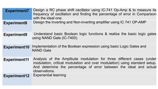
Experiment7 Design aRC phase shift oscillator using IC-741 Op-Amp & to measure its
frequency of oscillation and finding the percentage of error in Comparison
with the ideal one.
Experiment8 Design the Inverting and Non-inverting amplifier using IC 741 OP-AMP
Experiment9 Understand basic Boolean logic functions & realize the basic logic gates
using NAND Gate (IC-7400).
Experiment10 Implementation of the Boolean expression using basic Logic Gates and
NAND Gate
Experiment11 Analysis of the Amplitude modulation for three different cases (under
modulation, critical modulation and over modulation) using standard setup.
And determine the percentage of error between the ideal and actual
observations.
Experiment12 Experiential learning
16.
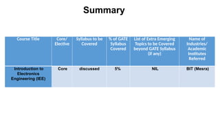
Summary
Course Title Core/
Elective
Syllabusto be
Covered
% of GATE
Syllabus
Covered
List of Extra Emerging
Topics to be Covered
beyond GATE Syllabus
(if any)
Name of
Industries/
Academic
Institutes
Referred
Introduction to
Electronics
Engineering (IEE)
Core discussed 5% NIL BIT (Mesra)