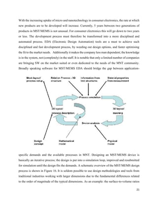
SlideShare a Scribd company logo
1
CHAPTER 1
INTRODUCTION
This report deals with the field of micro-electromechanical systems or MEMS. MEMS encompass
the process-based technologies used to fabricate tiny integrated devices and systems that integrate
functionalities from different physical domains into one device. Such devices are fabricated using
a wide range of technologies having in common the ability to create structures with micro-scale
and even Nano-scale accuracies. The products range in size from a few microns to millimeters.
These devices have the ability to sense, control and actuate on the micro scale and generate effects
on the macro scale. The interdisciplinary nature of MEMS relies on design, engineering and
manufacturing expertise from a wide and diverse range of technical areas including integrated
circuit fabrication technology, mechanical engineering, materials science, electrical engineering,
chemistry and chemical engineering, as well as fluid engineering, optics, instrumentation and
packaging. The complexity of MEMS is also seen in the extensive range of markets and
applications that incorporate such devices. MEMS can be found in systems ranging from consumer
electronics, automotive, medical, communication to defense applications. Current examples of
MEMS devices include accelerometers for airbag sensors, microphones, projection display chips,
blood and tire pressure sensors, optical switches, and analytical components such as lab-on-chip,
biosensors and many other products. This report introduces the field of MEMS and is divided into
five main sections. In the first two sections, the reader is introduced to MEMS, its definitions,
history, current and potential applications, as well as the state of the MEMS market and issues
concerning miniaturisation. The third section deals with the fabrication methods of MEMS
including photolithography, bulk micromachining, surface micromachining and high-aspect-ratio
micromachining. Assembly, system integration and packaging of MEMS devices are also
described here. The fourth section gives an overview of MEMS products. In the final section some
important trends in MEMS are discussed.
2
1.1 MEMS
MEMS, an acronym that originated in the United States, is also referred to as Micro System
Technology (MST) in Europe and Micromachining in Japan. Regardless of terminology, the
uniting factor of a MEMS device is in the way it is made. While the device electronics are
fabricated using `computer chip' IC technology, the micromechanical components are fabricated
by sophisticated manipulations of silicon and other substrates using micromachining processes.
Processes such as bulk and surface micromachining as well as high-aspect-ratio micromachining
(HARM) selectively remove parts of the silicon or add structural layers to form the mechanical
and electromechanical components. While integrated circuits are designed to exploit the electrical
properties of silicon, MEMS takes advantage of other material properties like optical, mechanical etc.
Within the wider field of MST we also see processes like micro moulding, laser ablation etc. used to create
microsystems components.
MEMS devices are very small; their components are usually microscopic. Pumps, valves,
gears, pistons, as well as motors and even steam engines have all been fabricated by MEMS.
However, two points are worth consideration. MEMS is not just about the miniaturisation of
mechanical components or making things out of silicon (in fact, the term MEMS is actually
misleading as many micro machined devices are not mechanical in a strict sense). MEMS is a
manufacturing technology; a paradigm for designing and creating complex integrated devices
and systems using batch fabrication techniques similar to the technologies used in IC
manufacturing or standard machining technologies extended in to the micro and nanometer
area. Secondly, not all miniaturized components are as yet useful or commercialised. Although
3
micro scale gearboxes, pumps and steam engines (see also Figure 1 and Figure 2) are
fascinating to see, the practical problems associated with the operating (wear, energy
efficiency etc.), and the high cost of creating them, often stands in the way of successful
commercialisation. From a very early vision in the early 1950's, MEMS has gradually made
its way out of research laboratories and into everyday products. In the mid-1990's, MEMS
components began appearing in numerous commercial products and applications including
accelerometers used to control airbag deployment in vehicles, pressure sensors for medical
applications, and inkjet printer heads. Later also other products were developed like:
oscillators, displays, lab on chip and microphones. MEMS has several distinct advantages as
a manufacturing technology. In the first place, the interdisciplinary nature of MEMS
technology and its micromachining techniques, as well as its diversity of applications has
resulted in an unprecedented range of devices and synergies across previously unrelated fields
(for example biology and microelectronics). Secondly, MEMS with its batch fabrication
techniques enables components and devices to be manufactured with increased performance
and reliability, combined with the obvious advantages of reduced physical size, volume,
weight and cost. Thirdly, MEMS provides the basis for the manufacture of products that cannot
be made by other methods. These factors make MEMS as pervasive technology as integrated
circuit microchips. However, three points makes it very different: MEMS products tend to be
application specific, giving rise to a wide range of very different products. Secondly, the
number of MEMS products will be always less than that for semiconductor IC’s. A good
example is the inkjet printer. The four inkjet nozzles are operated using printed circuit boards
with tens of other silicon devices. Thirdly, contrary to IC manufacturing, there is no such thing
as a standard building component like the transistor. This leads to a more diverse technology
base with more development and engineering work and therefore to a more expensive and
more difficult to maintain technology.
1.2 DEFINITION
This section defines some of the key terminology and classifications associated with MEMS.
It is intended to help the reader and newcomers to the field of micromachining become familiar
with some of the more common terms. A more detailed glossary of terms has been included in
Appendix A. Although MEMS are also referred to as MST, strictly speaking, MEMS is a
4
process technology used to create these tiny mechanical devices or systems, and as a result, it
is a subset of MST. There are considerable overlaps between fields in terms of their integrating
technology and their applications and hence it is extremely difficult to categorise MEMS
devices in terms of sensing domain and/or their subset of MST. The real difference between
MEMS and MST is that MEMS tends to use semiconductor processes to create a mechanical
part. In contrast, the deposition of a material on silicon for example, does not constitute a
MEMS product but is an application of MST. Micromachining relates to the creation of small
parts such as lenses, gearwheels etc. with mechanical functionality. Micro- opto-electro-
mechanical systems (MOEMS) are also a subset of MST and, together with MEMS, form the
specialized technology fields using combinations of miniaturized optics, electronics and
mechanics. Such microsystems incorporate the use of microelectronics batch processing
techniques for their design and fabrication. Such devices are used for scientific research, drug
development, clinical and point of care diagnostics, agriculture, food and environmental
monitoring. Biochips are broadly divided in microarray chips and microfluidics chips; the
microfluidics chips are also referred to as Lab-on-Chip: A complete micro-analytical device,
containing: pumps, valves, micro channels and reactors to manipulate test samples and other
reagents. Such chips also include a biosensor or an array of biosensors as well as a read-out
device. A capacitive pressure sensor measures a pressure by detecting an electrostatic
capacitance change; at least one electrode of the capacitor is on a moving structure. (See Figure
4). Capacitive sensors have the advantage over the piezoresistive type in that they consume
less power, but have a non-linear output signal and are more sensitive to electromagnetic
interference.
5
1.3 HISTORY
The history of MEMS is useful to illustrate its diversity, challenges and applications. The
following chronology summarizes some of the key MEMS milestones.
1950s 1958 Silicon strain gauges become commercially available.
1959 "There's plenty of room at the bottom" - Richard Feynman gives a keynote
presentation at California Institute of Technology. He issues a public challenge by
offering $1000 to the first person to create an electrical motor smaller than 1/64th of
an inch.
1960s 1961 First silicon pressure sensor demonstrated.
1967 Invention of surface micromachining. Westinghouse creates the Resonant Gate
Field Effect Transistor. Description of use of sacrificial material to free
micromechanical devices from the silicon substrate.
1970s 1970 First silicon accelerometer demonstrated.
1979 First micromachined inkjet nozzle.
1980s Early
1980s
First experiments in surface micromachined silicon.
1982 Disposable blood pressure transducer.
1982 "Silicon as a Mechanical Material". Instrumental paper to entice the scientific
community - reference for material properties and etching data for silicon.
1982 LIGA Process demonstrated.
Late
1980s
Micromachining leverages microelectronics industry and widespread
experimentation and documentation increases public interest.
1988 First MEMS conference.
1990s Novel methods of micromachining developed with an aim of improving sensors.
1992 MCNC starts the Multi-User MEMS Process (MUMPS) sponsored by Defense
Advanced
Research Projects Agency (DARPA).1992 First micro machined hinge and introduction of the Bosch DRIE process.
1993 First surface micromachined accelerometer sold (Analog Devices, ADXL50).
1994 Deep Reactive Ion Etching is patented.
1995 Bio MEMS rapidly develops.
2000s Massive industrialization and commercialization.
2001 Triaxis accelerometers appear on the market.
2002 First Nano imprinting tools announced.
2003 MEMS microphones for volume applications introduced.
6
1.4 APPLICATIONS, MARKETS, INDUSTRIALIZATION
High volume MEMS can be found in a diversity of applications across multiple markets (Table
1). In the context of emerging technologies, MEMS products were initially centred on
technology-product paradigms rather than product-market paradigms. Consequently, MEMS
devices have found numerous applications across a diversity of industries. For example,
MEMS accelerometer initially found a launching application in airbag sensors, from this they
were further developed to serve other applications in the automotive sector such as Electronic
Stability Program (ESP) and rollover detection. Thanks to technological advancements,
production costs went down and the sensors became affordable for consumer applications.
Parallel to this, accelerometers were introduced in high end applications such as medical pace
makers.
It is not within the scope of this report to detail all the current and potential applications within
each market segment, a selection of the most established MEMS devices is detailed instead
along with the potentially most significant future applications.
2003 Discera start sampling MEMS oscillators.
2004 TI’s DLP chip sales rose to nearly $900 million.
2005 Analog Devices shipped its two hundred millionth MEMS-based inertial sensor.
2006 Packaged triaxis accelerometers smaller then 10 mm3 are becoming available.
2006 Dual axis MEMS gyros appear on the market.
2006 Perpetuum releases vibration energy harvester.
7
CHAPTER 2
ESTABLISHED MEMS APPLICATIONS
2.1 Established mems applications
Automotive airbag sensors were one of the first commercial devices using MEMS. They are
in widespread use today in the form of a single chip containing a smart sensor, or
accelerometer, which measures the rapid deceleration of a vehicle on hitting an object. The
deceleration is transmitted by a change in voltage. An electronic control unit subsequently
sends a signal to trigger and explosively fill the protective airbag.
The accelerometer is essentially a capacitive or piezoresistive device consisting of a
suspended pendulum proof mass/plate assembly. As acceleration acts on the proof mass,
micromachined capacitive or piezoresistive plates sense a change in acceleration from
deflection of the plates. Environment as is found within a vehicle, proving the reliability of the
technology. An example of this success is witnessed in some of today's vehicles which have
over 75 MEMS devices including anti-lock braking systems, active suspension, appliance and
navigation control systems, vibration monitoring, fuel sensors, noise reduction, rollover
detection, seatbelt restraint and tensioning. As a result, the automotive industry has become
one of the main drivers for the development of MEMS often leading the way for other equally
or even more demanding environments.
The airbag sensor has been pivotal to the success of MEMS and micromachining technology.
With over a hundred million devices in production and sold in the last 15 years. It is worth
noting that such devices (see Figure 5 and Figure 6) are operating within such a challenging
8
2.2 Inkjet printer head
Probably the most successful MEMS product up till now is the inkjet printer head, superseding
even automotive and medical pressure sensors. Inkjet printers use a series of nozzles to spray
drops of ink directly on to a printing medium. Thermal inkjet Invented in 1979 by Hewlett-
Packard, MEMS thermal inkjet printer head technology relies on the thermal expansion of the
ink vapor. Within the printer head there is an array of tiny resistors acting as heaters. These
resistors can be fired under microprocessor control with electronic pulses of a few milliseconds
(usually less than 3 microseconds). Ink flows over each resistor, which when fired, heats up,
vaporizing the ink to form a bubble.
2.3 Overhead projection display
Texas Instruments (TI) began developing DLP (Digital Light Processor) MEMS products in
1987 and launched them in 1994, reaching the milestone of the first million to be shipped in
December 2001. Since then, the market has been growing at an increasing rate: from the second
million in August 2003, via the third million in April 2004 to the fifth million in December
2005. In 2006 the milestone of 10 million shipped DLP’s was surpassed.
2.4 Microphones
The first MEMS based microphones were developed in the eighties, but commercial success was
difficult to achieve due to it being a replacement product. The new devices had to compete with
9
very well entrenched traditional products such as the electret condenser microphone which is
inexpensive ($0.50 or less) and shows a good performance in terms of frequency response and
sensitivity. However, as MEMS microphones have the advantage of better temperature resistance,
they are therefore better suited for a highly automated assembly line; in contrast to the electret
condenser microphone, which have to be soldered by hand. Other advantages include the option
of integration with electronics and the ability to fabricate arrays into one chip. The main application
areas for such devices include digital cameras, mobile phones, electronic note books/pads, and
hands free sets of mobile phones in cars. Clearly hearing aids is also an important application area.
10
CHAPTER 3
COMMERCIALISATION AND INDUSTRIALISATION
3.1 Hybrid or Integration
 For many MEMS products, the ability to integrate with other electronic components is a
major advantage. Such a capability will lead to increased performance due to savings in
power consumption and increased performance, both associated with shorter lengths of
interconnections. This will also lead to a decrease in assembly cost.
Over the years MEMS products have been transformed from relatively simple components
for special applications to complex CMOS integrated devices for demanding, high volume,
applications. Associated with the choice of a technology platform for a specific product, is
a basic question, namely: Whether to adopt a hybrid design concept (CMOS and MST
structure on separate dies), or rely on monolithic integration (CMOS and MST structures
on one die)
Pro’s of the monolithic approach include:
 Fewer assembly steps.
 More compact designs.
 Lower parasitic loads of interconnects, often leading to optimal (sub) systems
characteristics.
 Mechanically more robust.
 Easier to protect against electromagnetic interference.
 Exploiting existing high volume capital infrastructure rather than building a specialized
line.
Con’s of the monolithic approach include:
 The development of the processing technology is time consuming and costly.
 For volume production the wafer processing is relatively costly.
 Only a few fabs offer this approach as an open access foundry service, compared with
the realm of specialized open
 Foundries for the hybrid approach, i.e. less choice, and less opportunity for second
sourcing.
11
 Constraints on either the MEMS processing and/or the circuitry processing, often leading
to less-than-optimal (sub-)
 Component characteristics.
Requires, in general, a larger design and simulation effort compared with the hybrid approach.
3.2 Quality and Standards
The MEMS industry is, in some respects, rather embryonic when compared to the more established
industries of microelectronics, semiconductors amongst others. In addition, and as emphasised
above, the multi-disciplinary nature of Micro and Nano Technologies (MNT) is specific to the
characteristics of this novel technology. Furthermore, the technologies and products are developed
to address a multi-market scenario. These characteristics, particular to MNT, make it very difficult
for standards to be set and followed within this industry. This applies equally to product
performance standards and to fabrication standards. The resultant scarcity of clear standards allows
operators to produce solutions (and products) which generally do not conform to wider system
requirements but dictate their own, and to slow integration, interaction and maintenance. Clearly,
organisations with influence and/or market monopoly tend to enforce their preferred solutions,
which may not be optimum for all users/buyers. Equally problematic are the small ventures, which
attempt to penetrate protected markets and an established way-of-doing-things. The lack of
fabrication standards is also a major issue worth noting. Processes used for MNT may not fall
within the realm of the well-established ones (particularly in the case of silicon processing). In
addition, as MNT products are unlikely to require full-time utilization of the production equipment,
such products will, generally, be consigned to a secondary priority relative to the main product of
a fabrication line. Also, in order to meet specific product requirements or to satisfy certain
customers, fabrication standards may not be followed, resulting in inconsistencies in quality. This
situation is difficult to control, particularly whilst MNT markets remain uncertain.
3.3 Technology and Commercialisation Hurdles
If someone had asked MEMS analysts 10 years ago, what the big challenge in MEMS was, most
people would had answered: commercialisation. Although technologically promising, MEMS was
difficult to sell: technology was not proven, there was no reliable infrastructure behind it and only
a few people understood the potential and were able to link the technology with a specific
12
application. Five years ago, the biggest issue was seen to be the industrialisation of the technology
and more specifically the packaging and integration. Having spent much time to bring the idea to
the market, developing core (chip based) technology and applications simultaneously, the package
was often neglected. Laboratory prototypes were difficult to translate to high-volume and low-cost
production concepts. Both issues have been improved considerably over the years: many MEMS
devices are on the market now and both specific and generic MEMS packages are increasingly
becoming available, especially for high volume sensors for automotive and consumer electronics.
Not all problems have disappeared though, as some of the attention has been shifted to the
following questions:
13
CHAPTER 4
FABRICATION TECHNIQUES
The variety and diversity of MST/MEMS products is huge. The Nexus Market Analysis for MEMS
and Microsystems III, 2005 – 2009 study1 named over 25 product groups, each containing several
different products for specific applications and markets, in total representing a $12 billion industry.
Each of these product groups relies on its own, often unique, technology.
To this end, service and equipment suppliers utilize a guide that clearly demonstrates the
technology roadmaps for these products. Such roadmaps will enable the supply chain to anticipate
developments and arrive at the right moment in time with the right solution. Industry-wide
roadmaps are possible when major industrial players work with commonly adopted technology
platforms. A good example of such a technology platform is CMOS technology in the
semiconductor industry. Here a limited and well known number of technology cha Contrary to the
semiconductor industry, the MST/MEMS industry does not show such a generic technology
platform that can be shared. Still, when studied in detail, some general trends become clearer and
it is possible to define, at least in general terms, the principle technology developments that
underpin MEMS fabrication. MEMS fabrication uses high volume IC style batch processing that
involves the addition or subtraction of two dimensional layers on a substrate (usually silicon) based
on photolithography and chemical etching. (See Figure 11) As a result, the 3-D aspect of MEMS
devices is due to patterning and interaction of the 2-D layers. Additional layers can be added using
a variety of thin-film deposition and bonding techniques as well as by etching through sacrificial
“spacer layers”. Llenges are defined as key issues for the industry. “Real” 3-D technologies
include high-aspect-ratio micromachining (HARM), such as LIGA (a German acronym from
Lithography, Galvanoformung, Abformung translated as lithography, electroforming and
moulding, see Figure 20); but also conventional macroscale manufacturing techniques such as
injection moulding, turning, drilling etc, are all good for producing three dimensional shapes and
objects, but limited to low complexity products. MEMS fabrication uses high volume IC style
14
batch processing that involves the addition or subtraction of two dimensional layers on a substrate
(usually silicon) based on photolithography and chemical etching. (See Figure 12) As a result, the
3-D aspect of MEMS devices is due to patterning and interaction of the 2-D layers. Additional
layers can be added using a variety of thin-film deposition and bonding techniques as well as by
etching through sacrificial “spacer layers”.
4.1 Substrates
Silicon is still by far the most commonly used substrate in microelectronics and micro technology,
particularly by the semiconductor industry. Silicon wafer area shipments total more than 5 billion
square inches per year. The silicon commonly used for substrates has a purity befitting the demand
and is doped to provide the required electronic properties. The success of silicon is based first on
its excellent electronic characteristics, and also on its chemical and mechanical properties. Silicon
forms the same type of crystal structure as diamond (see Figure 21), and although the interatomic
bonds are much weaker, it is harder than most metals. In addition, it is surprisingly resistant to
mechanical stress, having a higher elastic limit than steel in both tension and compression. Single
15
crystal silicon also remains strong under repeated cycles of tension and compression. The
crystalline orientation of silicon is important in the fabrication of MEMS devices because some of
the etchants used attack the crystal at different rates in different directions MST/MEMS designers
are increasingly using SOI (Silicon on Insulator) wafers. Such wafers consist of two layers of
silicon separated by a thin silicon oxide layer. To create free-hanging silicon structures the top
layer is used as a mechanical device part and the silicon insulating layer as the underlying
sacrificial layer. From a processing perspective, the disadvantage of using glass for standard
waferfabs is the higher sensitivity to thermal and mechanical shock. When the edges of the wafers
are crack free however, this does not need to be such a problem as is often feared. A more difficult
problem lies in the automatic handling of glass based wafers by most of the production equipment.
Such equipment mainly uses optical sensors to detect the presence of a wafer. The transparency of
the glass-based wafer, however, prohibits their detection. For large production numbers, moulding
is by far the most economically attractive fabrication technology. For smaller numbers, the tool
setup cost is often too high and powder blasting or wet etch offer more cost effective alternatives.
Mechanical processing and photo imageable glass are relatively expensive technologies and are
only used for small quantities. For large volumes wet chemical etching and powder blasting are
the technologies of choice. There is a well-developed supply chain for glass processing. Many
companies can process the glass wafers using some of the above listed techniques, and an
increasing number of suppliers are able to handle glass wafers in their facilities. The concept of
creating 3-D packages by mounting thin structured silicon (or glass) wafers on top of each other
has increased the interest in very thin silicon wafers. Thinning of silicon wafers has a long history
in semiconductors to enable the creation of thin packaged components of interest for i.e. mobile
phones where space is limited. Wafer thinning is also required for applications such as smart cards
and in the production of SOI wafers. Continuous improvement of processes and equipment has
resulted in achieving wafer thicknesses as low as 50 μm in production.
4.2 Planar Technologies
The planar technologies are mostly based on semiconductor technologies like photolithography,
sputtering, evaporating, Low Pressure Chemical Vapour Deposition (LPCVD), Plasma Enhanced
Chemical Vapour Deposition (PECVD), wet and dry etching, and chemical mechanical
planarisation. To those technologies some specific MEMS technologies are added like bulk and
16
surface machining; waferbonding; backside alignment, Deep Reactive Ion Etching (DRIE) etc.
The most important specific MEMS processes are discussed below.
4.3 Photolithography
Photolithography is the photographic technique to transfer copies of a master pattern, usually a
circuit layout in IC applications, onto the surface of a substrate of some material (usually a silicon
wafer). For example, the substrate is covered with a thin film of some material, usually silicon
dioxide (SiO2), in the case of silicon wafers, on which a pattern of holes will be formed. A thin
layer of an organic polymer, which is sensitive to ultraviolet radiation, is then deposited on the
oxide layer; this is called a photoresist. A photomask, consisting of a glass plate (transparent)
coated with a chromium pattern (opaque), is then placed in contact with the photoresist coated
surface. The wafer is exposed to the ultraviolet radiation transferring the pattern on the mask to
the photoresist which is then developed in a way very similar to the process used for developing
photographic films. The radiation causes a chemical reaction in the exposed areas of the photoresist
of which there are two types; positive and negative. (See also Figure 19 and Figure 20). Positive
photoresist is weakened by UV radiation whereas negative photoresist is strengthened. On
developing, the rinsing solution removes either the exposed areas or the unexposed areas of
photoresist leaving a pattern of bare and photoresist- coated oxides on the wafer surface. The
resulting photoresist pattern is either the positive or negative image of the original pattern of the
photomask. A special chemical is used to attack and remove the uncovered oxide from the exposed
areas of the photoresist. The remaining photoresist is subsequently removed, leaving a pattern of
oxide on the silicon surface. The final oxide pattern is either a positive or negative copy of the
photomask pattern and can serve as a mask in subsequent processing steps.
Besides those standard resists, there are three kinds of special resists used for MST/MEMS:
• Thick resist, used when high aspect ratio electroplated material is required (LIGA or HARMST
processing).
• Nano-imprint resist. Nano imprinting uses pressure to structure the resist instead of or in addition
to (UV) light. Electro-deposition resist, used for wafers featuring a large topography.
17
Lately there has been an increasing interest for technologies enabling deposition of resist without
the need for alignment and developing. The reason is not so much the potential savings on
processing and material cost, nor even the savings on process time, but the fact that those
technologies can deposited resist on some areas, without damaging other areas containing sensitive
parts as in the case of biosensors or freehanging structures. Front to back alignment In many cases
MEMS devices are fabricated by processing two sides of a wafer. For instance a pressure sensor
is made by defining the sensing element on the front side and the membrane is formed by etching
from the back. This needs careful alignment of the structures on the back to the structures on the
front during lithography. Equipment for front to back alignment
4.4 Etching
In bulk and surface micromachining silicon etching is an important step. Not only for creating the
base structures like trenches and cavities, but also for the final release of the membranes,
cantilevers or free hanging masses in surface micromachining. This final release etching or
sacrificial etching involves the undercutting by etching of a structure. The two processes are shown
in the next picture:
4.5 Wet Etching
Wet etching describes the removal of material through the immersion of a material (typically a
silicon wafer) in a liquid bath of a chemical etchant. These etchants can be isotropic or anisotropic.
Isotropic etchants etch the material at the same rate in all directions, and consequently remove
material under the etch masks at the same rate as they etch through the material; this is known as
undercutting (Figure 14a and b). Etch rates can slow down and in some cases (for example, in deep
18
and narrow channels) they can stop due to diffusion limiting factors. However, this effect can be
minimized by agitation of the etchant, resulting in structures with near perfect and rounded
surfaces (Figure 14b-). Isotropic etchants are limited by the geometry of the structure to be etched.
Anisotropic etchants etch faster in a preferred direction. Potassium hydroxide (KOH) is the most
common anisotropic etchant as it is relatively safe to use. Structures formed in the substrate by
using this etchant are dependent on the crystal orientation of the substrate or wafer. They progress
rapidly Isotropic etchants are limited by the geometry of the structure to be etched. Anisotropic
etchants etch faster in a preferred direction. Potassium hydroxide (KOH) is the most common
anisotropic etchant as it is relatively safe to use. Structures formed in the substrate by using this
etchant are dependent on the crystal orientation of the substrate or wafer. They progress rapidly
4.6 Dry Etching
Dry etching relies on vapour phase or plasma-based methods of etching using suitably reactive
gases or vapours usually at high temperatures. The two most common special dry MEMS etches
are xenon difluoride (XeF2) etching. It is an isotropic silicon etch process and has a strong
selectivity for silicon above Al, SiO2, Si3N4 and photoresist. The typical etch rates are 1 to 3
μm/min and it is commonly used for release etch. The other is Reactive Ion Etching (RIE) which
utilizes additional energy in the form of radio frequency (RF) power to drive the chemical reaction.
Energetic ions are accelerated towards the material to be etched supplying the additional energy
needed for the reaction; as a result the etching can occur at much lower temperatures (typically
19
150º - 250ºC, sometimes room temperature or even lower) than those usually needed (above
500ºC). RIE is not limited by the crystal planes in the silicon, and as a result, deep trenches and
pits, or arbitrary shapes with vertical walls can be etched. The MEMS process Deep Reactive Ion
Etching (DRIE) is a much higher-aspect-ratio etching method. It involves an alternating process
of high-density plasma etching (as in RIE) and protective polymer deposition to achieve greater
aspect ratios.
4.7 CMP (Chemical Mechanical Planarisation)
Chemical Mechanical Polishing (CMP) was first developed by IBM to enable lithography on
multi-layer stacks. Due to the differences in surface height focus problems arose in next
lithography steps, in this way making further miniaturisation impossible. At this moment CMP is
worldwide accepted as a cleanroom process that is inevitable in the production of integrated
circuits. Originally developed for the planarisation of SiO2 surfaces only, the CMP spectrum has
broadened to a wide variety of processes including metal CMP like copper damascene.
20
CHAPTER 5
DESIGN AND MODELLING
21
With the increasing uptake of micro and nanotechnology in consumer electronics, the rate at which
new products are to be developed will increase. Currently, 5 years between two generations of
products in MST/MEMS is not unusual. For consumer electronics this will go down to two years
or less. The development process must therefore be transformed into a more disciplined and
automated process. EDA (Electronic Design Automation) tools are a must to achieve such
disciplined and fast development process, by weeding out design options, and faster optimising
the fit to the market needs. Additionally it makes the company less man dependent; the knowledge
is in the system, not (completely) in the staff. It is notable that only a limited number of companies
are bringing SW on the market suited or even dedicated to the needs of the MNT community.
Broadly speaking software for MST/MEMS EDA should bridge the gap between application-
specific demands and the available processes in MNT. Designing an MST/MEMS device is
basically an iterative process; the design is put into a simulation loop, improved and resubmitted
for simulation until the design fits the demands. A schematic overview of the MST/MEMS design
process is shown in Figure 16. It is seldom possible to use design methodologies and tools from
traditional industries working with larger dimensions due to the fundamental differences related
to the order of magnitude of the typical dimensions. As an example: the surface-to-volume ratios
22
are different in the micro world from what they are in the macro world. In the macro world,
thickness of a structure is often comparable in size to length and width, but most micro devices are
very thin and therefore some dimensions can be out of scale to the others. Electrostatic forces and
fluid damping effects are also different; they be can significantly larger. Furthermore, the analysis
of MEMS is particularly challenging due to the need to confront a large number of issues. In the
macro world, engineers have to consider only one or two physical domains. In MST/MEMS,
designers must take several domains into account during the course of a design session.
5.1 Packaging
Selecting the proper technology may tip the scales towards a product success or towards a product
failure. This is especially valid for packaging, as this nearly always represents a substantial part of
the cost of the product. It is therefore not a marginal concern, but a crucial part of the product
design. Packaging and assembly for MST/MEMS has long been a neglected area. Lately more
companies entered this field. They range from small start-ups, offering very specialized services,
to large semiconductor packaging companies, having production lines for microsystem-based
products. Much effort has been put into the modification of well proven semiconductor package
concepts for use in MNT. With the increased availability of MEMS processes with make the
products fit into more of less standard packages, the old wisdom that the package in MEMS takes
about 80% or more of the total cost doesn’t apply anymore. Even a full hermitic ceramic package
is available in the range and low cost packages like QFN are even down to 0,10 . Injection
moulding packages are in the 0, 08 -0, 15 range. Although the capping cost can be substantial, the
packaging part of the total cost is now on par or even below the chip cost for a number of high
volume products. A MEMS oscillators is reputed to be packaged in a QFN package for les then
with the increased availability of MEMS processes with make the products fit into more of less
standard packages, the old wisdom that the package in MEMS takes about 80% or more of the
total cost doesn’t apply anymore. Even a full hermitic ceramic package is available in the range
and low cost packages like QFN are even down to 0,10 . Injection moulding packages are in the
0, 08 -0, 15 range. Although the capping cost can be substantial, the packaging part of the total
23
cost is now on par or even below the chip cost for a number of high volume products. A MEMS
oscillators is reputed to be packaged in a QFN package for les then 0,1
5.2 MEMS Packaging Platforms
Metal can and ceramic packages typical examples are metal can packages and ceramic packages.
They are relatively easy to use for MEMS products. Metal can packages provide excellent thermal
dissipation and electromagnetic shielding, ceramic packages are ideally suited for fragile dies and
low volumes. Optical products, such as IR sensors or routing switches are a little more difficult to
assemble when compared to accelerometers. Such devices share the sensitivity problems but also
need optical access through the package. Thus, it is necessary to ensure the transparency of the
package as well as the operational reliability of the mechanical microstructures, throughout their
lifetime. In such cases, vacuum or special gas filling might be used. This leads to hermeticity
demands for the package, although getters (often metals or zeolites) can be used. The simplest way
to satisfy such demands is to utilize a ceramic package and use a transparent lid (“porthole”) to
close/seal the package.
24
5.3 Reliability and Test
The rising complexity of products, the increasing amount of functionalities in one package and the
multi-domain operation of MNT-based devices makes the testing and the design for reliability of
new products a real challenge. When new types of MNT- based systems are developed new failure
modes turn up and the situation becomes even more complex for those systems that operate in
different domains simultaneously. On top of that, those domains often interact. Especially difficult
to test are disposable products – they cannot be fully tested and a test of 1M components does not
say the 1,000,001st will work. Reliability is only in few cases addressed during the design phase;
often manufacturers will only worry about the risks after experiencing yield problems or if
problems are encountered during the use of the products.
Although we tend to speak about MNT products in general, different markets have different needs.
For instance:
 For consumer applications the highest priority is low cost. Consumer applications ask for high
yield and low-cost test, which demands for robust design and processing. The lifetime of a product
is relatively short and a limited number of lifetime failures are acceptable. Consumer products are
often mistreated by users, thus some general robustness is required.
CHAPTER 6
25
THE FUTURE OF MEMS
The future of MEMS is integrally linked to market trends in general and driven by the increasing
demand to monitor and control our environment and the equipment and instruments we use in our
daily lives. This demand does, undoubtedly, lead to the need for more sensors in cars, more sensors
in industrial equipment and installation and, more sensors for our ambient intelligence. In order to
avoid the need for a multitude of wires, such sensors must be self-sustaining and able to
communicate wirelessly. As a result, not only more sensors are needed, but also small energy
generating modules and wireless transmission components. Clearly, the increased numbers of
devices will drive size reduction which in turn will enable higher levels of integration. Studies also
show that there is an increasing trend to spend on health care, due to the growing numbers of
elderly people in developed countries and a growing medical and pharmaceutical infrastructure in
developing countries. There is also a trend to transfer diagnostics from the central analytical
laboratory to a surgeries or clinics that are smaller and closer to the patients. This fuels a growing
demand for small and affordable devices for diagnostics, especially for point of care diagnostics.
In addition, national security is of increased importance related to the growing fear from terrorist
attacks and outbreaks of infectious human or animal diseases. This drives a need for small multi
parameter instruments to test air, water blood etc. for microbiological threats. Simultaneously there
are some general technical trends which will influence the MEMS industry. In the first place the,
long awaited, ending of the Moore’s law will lead to an increasing attention in the IC industry for
other ways to improve the performance of ICs. The so called Moore than Moore trend will add
new technologies to the rather mono cultural landscape of semiconductors to enable extra
functionalities, to exploring further miniaturization by using die stacking etc.. There is also a
tendency to explore more flexible and more affordable production technologies. This will be
driven by the production research into typical low cost, large surface area devices like solar cell,
displays, wearable electronics and disposable diagnostics devices. (Re) introduction of printing
technologies is one of the possibilities, low cost substrates like plastics are another. Last but not
least, a plethora of products will come from the large amount of nanotechnology research
26
6.1 Small, self-sustaining, wireless sensor networks
As discussed above, the most important market trends are those reliant on merging functionalities
in products such as cameras, music players, computing, mobile phones, and portable consumer
electronics in general, as well as the merging of MST/MEMS technologies with high volume
electronics. In this context, some examples of MST/MEMS products being one general technology
trend is especially worth mentioning: the increasing use of sensors and other small electronic
devices in and around our direct environment. We will be surrounded by more electronics and will
be interacting more with such intelligence. This creates a need for smaller and cheaper electronic
products, which are energy efficient and self-sustaining as well as able to communicate via
wireless with other electronic devices. Devices suitable for new applications connected to ambient
intelligence and ultimately expected to be used are smart dust (see next Figure). The big advantage
of wireless sensor systems is that by removing wires and batteries, there is the potential for
embedding sensors in previously inaccessible locations; it also becomes feasible to use a large
numbers of sensors because there is no longer the need for regular replacement or recharging of
batteries.
27
6.2 Medical diagnostic devices
A shift from clinical to point of care diagnostics, accompanied by a slow but significant drift from
medical diagnostics to more lifestyle oriented diagnostics: allergy, drugs, cholesterol, alcohol, but
also diagnostics in sport . This together will make this market more consumer-oriented. Therefore
perhaps the fastest growing market for MEMS with many interesting applications for Point of Care
monitoring, of which glucose level monitoring will represent the largest single segment. Cheap
disposable sensors are regarded as the sweet spot in diagnostics.
6.3 DNA chips
DNA chips have been commercialized by many companies, and a range of equipment is available
for DNA chip sample processing, data analysis etc. Future lab-on-a-chip technology may include
implantable “pharmacy-on-a-chip” devices precisely and timely releasing drugs into a body,
without needing needles or injections. The delivery of insulin is one such application, as is the
delivery of hormones, chemotherapy drugs and painkillers. First generation devices are being
developed which release their medication upon signals from an outside source, wired through the
skin. Proposed second generation devices may be wireless and third generation MEMS chips could
interact with MEMS sensors embedded in the body to respond to the body’s own internal signals.
6.4 Other microfluidic devices
Furthermore, there are many uses expected for microfluidics in all kind of analytical equipment
such as mass spectrometry and chromatography. A microfluidics platform integrates sample
definition, injector, detectors and diagnostics leading to fast analysis, increased ease of use,
handheld and remote operation. They will not only be used for home defence, but also for
environmental measurements and industrial process control.
28
CONCLUSION
It made me more aware of the scope of Electronics & Communication Engineering. It has also
made me appreciative of an industrial work environment.
Undergoing this seminar has helped me integrate conceptual knowledge with real life
application. I was fortunate to have personal guidance from experienced professionals who took
been interest in explaining the working details of various equipments.
I feel that without this opportunity, my own understanding of this subject and also the
motivation to acquire more knowledge would have remained incomplete. Well, regarding future
scope
“To know the technical know-how, seminar is the best way to move forward.”

More Related Content

What's hot

Introduction to mems
Introduction to memsIntroduction to mems
Introduction to memsKaushal Pant
 
AIR BAG CRASH USING MEMS
AIR BAG CRASH USING MEMS AIR BAG CRASH USING MEMS
AIR BAG CRASH USING MEMS Ganesh Gani
 
Mems(Intro Presentation)
Mems(Intro Presentation)Mems(Intro Presentation)
Mems(Intro Presentation)Vinayak Hegde
 
Mems and sensors packaging technology and trends presentation held by Amandin...
Mems and sensors packaging technology and trends presentation held by Amandin...Mems and sensors packaging technology and trends presentation held by Amandin...
Mems and sensors packaging technology and trends presentation held by Amandin...Yole Developpement
 
Embedded Systems Training Report
Embedded Systems Training ReportEmbedded Systems Training Report
Embedded Systems Training ReportAkhil Garg
 
Micro pumps & micro valves
Micro pumps & micro valvesMicro pumps & micro valves
Micro pumps & micro valvesAhmed Elsayes
 
Mems pressure sensor project report
Mems pressure sensor project reportMems pressure sensor project report
Mems pressure sensor project reportBabul Kumar
 
Micro electro mechanical systems
Micro electro mechanical systemsMicro electro mechanical systems
Micro electro mechanical systemssree navya
 
Bio-Molecular computers
Bio-Molecular computersBio-Molecular computers
Bio-Molecular computersMoumita Kanrar
 
MEMS & Sensors challenges & opportunities for the next decade 2016 Presentati...
MEMS & Sensors challenges & opportunities for the next decade 2016 Presentati...MEMS & Sensors challenges & opportunities for the next decade 2016 Presentati...
MEMS & Sensors challenges & opportunities for the next decade 2016 Presentati...Yole Developpement
 

What's hot (20)

Introduction to mems
Introduction to memsIntroduction to mems
Introduction to mems
 
Mems ppt
Mems pptMems ppt
Mems ppt
 
AIR BAG CRASH USING MEMS
AIR BAG CRASH USING MEMS AIR BAG CRASH USING MEMS
AIR BAG CRASH USING MEMS
 
Mems technology
Mems technologyMems technology
Mems technology
 
Mems(Intro Presentation)
Mems(Intro Presentation)Mems(Intro Presentation)
Mems(Intro Presentation)
 
Mems (Report)
Mems (Report)Mems (Report)
Mems (Report)
 
Mems and sensors packaging technology and trends presentation held by Amandin...
Mems and sensors packaging technology and trends presentation held by Amandin...Mems and sensors packaging technology and trends presentation held by Amandin...
Mems and sensors packaging technology and trends presentation held by Amandin...
 
Mems technology
Mems technologyMems technology
Mems technology
 
Electons meet animals
Electons meet animalsElectons meet animals
Electons meet animals
 
Embedded Systems Training Report
Embedded Systems Training ReportEmbedded Systems Training Report
Embedded Systems Training Report
 
final smart dust PPT
final smart dust PPTfinal smart dust PPT
final smart dust PPT
 
Mems in medical technology
Mems in medical technologyMems in medical technology
Mems in medical technology
 
Lecture 02 history & characteristics of mems
Lecture 02   history & characteristics of memsLecture 02   history & characteristics of mems
Lecture 02 history & characteristics of mems
 
Micro pumps & micro valves
Micro pumps & micro valvesMicro pumps & micro valves
Micro pumps & micro valves
 
Mems process
Mems processMems process
Mems process
 
Mems pressure sensor project report
Mems pressure sensor project reportMems pressure sensor project report
Mems pressure sensor project report
 
Micro electro mechanical systems
Micro electro mechanical systemsMicro electro mechanical systems
Micro electro mechanical systems
 
Bio-Molecular computers
Bio-Molecular computersBio-Molecular computers
Bio-Molecular computers
 
MEMS & Sensors challenges & opportunities for the next decade 2016 Presentati...
MEMS & Sensors challenges & opportunities for the next decade 2016 Presentati...MEMS & Sensors challenges & opportunities for the next decade 2016 Presentati...
MEMS & Sensors challenges & opportunities for the next decade 2016 Presentati...
 
optical computers
optical computersoptical computers
optical computers
 

Viewers also liked

Micro Electro Mechanical systems
Micro Electro Mechanical systemsMicro Electro Mechanical systems
Micro Electro Mechanical systemsVinodh Yadav
 
Micromachining of poly (methyl
Micromachining of poly (methylMicromachining of poly (methyl
Micromachining of poly (methylantjjournal
 
Choice of laser sources for micromachining applications
Choice of laser sources for micromachining applicationsChoice of laser sources for micromachining applications
Choice of laser sources for micromachining applicationsJK Lasers
 
MEMS Technology & its application for Miniaturized Space System
MEMS Technology & its application for Miniaturized Space SystemMEMS Technology & its application for Miniaturized Space System
MEMS Technology & its application for Miniaturized Space SystemIJSRD
 
Automotive transient thermal modeling seminar draft 5
Automotive transient thermal modeling seminar draft 5Automotive transient thermal modeling seminar draft 5
Automotive transient thermal modeling seminar draft 5Jonathan Earley
 
Nuclear thermal propulsion in space(NTP)
Nuclear thermal propulsion in space(NTP)Nuclear thermal propulsion in space(NTP)
Nuclear thermal propulsion in space(NTP)SANDIP THORAT
 
virtual manufacturing seminar repot
virtual manufacturing seminar repotvirtual manufacturing seminar repot
virtual manufacturing seminar repotAnusha Chethana
 
PAPER ON MEMS TECHNOLOGY
PAPER ON MEMS TECHNOLOGYPAPER ON MEMS TECHNOLOGY
PAPER ON MEMS TECHNOLOGYDhaval Kaneria
 
Seminar on magnetic levitation (maglav)
Seminar on magnetic levitation (maglav)Seminar on magnetic levitation (maglav)
Seminar on magnetic levitation (maglav)Yash Srivastava
 
Gasoline direct-injection
Gasoline direct-injectionGasoline direct-injection
Gasoline direct-injectionShiba Mohapatra
 
Plc & scada seminar
Plc & scada seminarPlc & scada seminar
Plc & scada seminarMayank Verma
 

Viewers also liked (20)

Micro Electro Mechanical systems
Micro Electro Mechanical systemsMicro Electro Mechanical systems
Micro Electro Mechanical systems
 
mems ppt
mems pptmems ppt
mems ppt
 
Micromachining of poly (methyl
Micromachining of poly (methylMicromachining of poly (methyl
Micromachining of poly (methyl
 
Choice of laser sources for micromachining applications
Choice of laser sources for micromachining applicationsChoice of laser sources for micromachining applications
Choice of laser sources for micromachining applications
 
ABHISHEK
ABHISHEKABHISHEK
ABHISHEK
 
MEMS Technology & its application for Miniaturized Space System
MEMS Technology & its application for Miniaturized Space SystemMEMS Technology & its application for Miniaturized Space System
MEMS Technology & its application for Miniaturized Space System
 
Nova engine powerpoint
Nova engine powerpointNova engine powerpoint
Nova engine powerpoint
 
21275
2127521275
21275
 
Automotive transient thermal modeling seminar draft 5
Automotive transient thermal modeling seminar draft 5Automotive transient thermal modeling seminar draft 5
Automotive transient thermal modeling seminar draft 5
 
Nuclear thermal propulsion in space(NTP)
Nuclear thermal propulsion in space(NTP)Nuclear thermal propulsion in space(NTP)
Nuclear thermal propulsion in space(NTP)
 
virtual manufacturing seminar repot
virtual manufacturing seminar repotvirtual manufacturing seminar repot
virtual manufacturing seminar repot
 
Mems finalr eport
Mems finalr eportMems finalr eport
Mems finalr eport
 
PAPER ON MEMS TECHNOLOGY
PAPER ON MEMS TECHNOLOGYPAPER ON MEMS TECHNOLOGY
PAPER ON MEMS TECHNOLOGY
 
Seminar on magnetic levitation (maglav)
Seminar on magnetic levitation (maglav)Seminar on magnetic levitation (maglav)
Seminar on magnetic levitation (maglav)
 
Gasoline direct-injection
Gasoline direct-injectionGasoline direct-injection
Gasoline direct-injection
 
Plc & scada seminar
Plc & scada seminarPlc & scada seminar
Plc & scada seminar
 
OTEC Seminar Report
OTEC Seminar  Report OTEC Seminar  Report
OTEC Seminar Report
 
FUEL ENERGIZER
FUEL ENERGIZER FUEL ENERGIZER
FUEL ENERGIZER
 
Green engine
Green engineGreen engine
Green engine
 
Mems technology ppt
Mems technology pptMems technology ppt
Mems technology ppt
 

Similar to MEMS technology technical seminar report

Week 7 - Course Project Draft - Gagandeep Bedi
Week 7 - Course Project Draft - Gagandeep BediWeek 7 - Course Project Draft - Gagandeep Bedi
Week 7 - Course Project Draft - Gagandeep Bedigsb100
 
Introduction to mems
Introduction to memsIntroduction to mems
Introduction to memsKaushal Pant
 
Micro-Electromechanical Systems (Mems)
Micro-Electromechanical Systems (Mems)Micro-Electromechanical Systems (Mems)
Micro-Electromechanical Systems (Mems)IJMER
 
Micro Electro-mechanical system
Micro Electro-mechanical systemMicro Electro-mechanical system
Micro Electro-mechanical systemMohit Singh Rajput
 
Mems project by abhishek mahajan
Mems project by abhishek mahajanMems project by abhishek mahajan
Mems project by abhishek mahajanAbhishek Mahajan
 
dokumen.tips_mems-technology-55846320a5038.ppt
dokumen.tips_mems-technology-55846320a5038.pptdokumen.tips_mems-technology-55846320a5038.ppt
dokumen.tips_mems-technology-55846320a5038.pptsanjaykj6
 
Mems technologies and analysis of merits and demerits
Mems technologies and analysis of merits and demeritsMems technologies and analysis of merits and demerits
Mems technologies and analysis of merits and demeritsBiprasish Ray
 
MEMS and Solar Sail for Space Application
MEMS and Solar Sail for Space ApplicationMEMS and Solar Sail for Space Application
MEMS and Solar Sail for Space ApplicationRamesh Tholiya
 
Micro electro mechanical systems (MEMS)....pptx
Micro electro mechanical systems (MEMS)....pptxMicro electro mechanical systems (MEMS)....pptx
Micro electro mechanical systems (MEMS)....pptxcharangowdakn17
 
An Introduction to MEMS (Micro-electromechanical Systems) (2002).pdf
An Introduction to MEMS (Micro-electromechanical Systems) (2002).pdfAn Introduction to MEMS (Micro-electromechanical Systems) (2002).pdf
An Introduction to MEMS (Micro-electromechanical Systems) (2002).pdfCaeluM4
 
Micro electro mechanical systems (MEMS) (1).pptx
Micro electro mechanical systems (MEMS) (1).pptxMicro electro mechanical systems (MEMS) (1).pptx
Micro electro mechanical systems (MEMS) (1).pptxsmanjunarayana
 
MEMS_and_microsystems_design_manufacture (1).pdf
MEMS_and_microsystems_design_manufacture (1).pdfMEMS_and_microsystems_design_manufacture (1).pdf
MEMS_and_microsystems_design_manufacture (1).pdfDrRishiJP
 

Similar to MEMS technology technical seminar report (20)

Week 7 - Course Project Draft - Gagandeep Bedi
Week 7 - Course Project Draft - Gagandeep BediWeek 7 - Course Project Draft - Gagandeep Bedi
Week 7 - Course Project Draft - Gagandeep Bedi
 
Introduction to mems
Introduction to memsIntroduction to mems
Introduction to mems
 
Microelectronic mechanical system
Microelectronic mechanical systemMicroelectronic mechanical system
Microelectronic mechanical system
 
MEMS Chapter 2
MEMS Chapter 2MEMS Chapter 2
MEMS Chapter 2
 
Mems
MemsMems
Mems
 
Micro-Electromechanical Systems (Mems)
Micro-Electromechanical Systems (Mems)Micro-Electromechanical Systems (Mems)
Micro-Electromechanical Systems (Mems)
 
Micro Electro-mechanical system
Micro Electro-mechanical systemMicro Electro-mechanical system
Micro Electro-mechanical system
 
Mems project by abhishek mahajan
Mems project by abhishek mahajanMems project by abhishek mahajan
Mems project by abhishek mahajan
 
NEMS MEMS PAPER
NEMS MEMS PAPERNEMS MEMS PAPER
NEMS MEMS PAPER
 
dokumen.tips_mems-technology-55846320a5038.ppt
dokumen.tips_mems-technology-55846320a5038.pptdokumen.tips_mems-technology-55846320a5038.ppt
dokumen.tips_mems-technology-55846320a5038.ppt
 
Mems technologies and analysis of merits and demerits
Mems technologies and analysis of merits and demeritsMems technologies and analysis of merits and demerits
Mems technologies and analysis of merits and demerits
 
MEMS and Solar Sail for Space Application
MEMS and Solar Sail for Space ApplicationMEMS and Solar Sail for Space Application
MEMS and Solar Sail for Space Application
 
Micro electro mechanical systems (MEMS)....pptx
Micro electro mechanical systems (MEMS)....pptxMicro electro mechanical systems (MEMS)....pptx
Micro electro mechanical systems (MEMS)....pptx
 
An Introduction to MEMS (Micro-electromechanical Systems) (2002).pdf
An Introduction to MEMS (Micro-electromechanical Systems) (2002).pdfAn Introduction to MEMS (Micro-electromechanical Systems) (2002).pdf
An Introduction to MEMS (Micro-electromechanical Systems) (2002).pdf
 
Mems ppt
Mems pptMems ppt
Mems ppt
 
1_MEMS - Introduction.pdf
1_MEMS - Introduction.pdf1_MEMS - Introduction.pdf
1_MEMS - Introduction.pdf
 
Micro electro mechanical systems (MEMS) (1).pptx
Micro electro mechanical systems (MEMS) (1).pptxMicro electro mechanical systems (MEMS) (1).pptx
Micro electro mechanical systems (MEMS) (1).pptx
 
Mems presentation
Mems presentationMems presentation
Mems presentation
 
MEMS_and_microsystems_design_manufacture (1).pdf
MEMS_and_microsystems_design_manufacture (1).pdfMEMS_and_microsystems_design_manufacture (1).pdf
MEMS_and_microsystems_design_manufacture (1).pdf
 
ME189_Chapter 1.pdf
ME189_Chapter 1.pdfME189_Chapter 1.pdf
ME189_Chapter 1.pdf
 

More from ravi kant

smart meter technical seminar report
smart meter technical seminar reportsmart meter technical seminar report
smart meter technical seminar reportravi kant
 
Smart energy metering system
Smart energy metering systemSmart energy metering system
Smart energy metering systemravi kant
 
indian railway training report
indian railway training reportindian railway training report
indian railway training reportravi kant
 
BSNL training report
BSNL training reportBSNL training report
BSNL training reportravi kant
 
kota thermal power plant
kota thermal power plantkota thermal power plant
kota thermal power plantravi kant
 
RRVUN hydro power plant
RRVUN hydro power plantRRVUN hydro power plant
RRVUN hydro power plantravi kant
 
Vedanta Hindustan zinc training
Vedanta Hindustan zinc trainingVedanta Hindustan zinc training
Vedanta Hindustan zinc trainingravi kant
 
Thermal power plant
Thermal power plantThermal power plant
Thermal power plantravi kant
 
Ntpc kahalgaon training report
Ntpc kahalgaon training reportNtpc kahalgaon training report
Ntpc kahalgaon training reportravi kant
 
Circuit breaker presentation
Circuit breaker presentationCircuit breaker presentation
Circuit breaker presentationravi kant
 
Aditya birla cement training report
Aditya birla cement training reportAditya birla cement training report
Aditya birla cement training reportravi kant
 
Hindustan zinc report
Hindustan zinc reportHindustan zinc report
Hindustan zinc reportravi kant
 
Hindustan zinc report
Hindustan zinc reportHindustan zinc report
Hindustan zinc reportravi kant
 
grid sub-station training Report
grid sub-station training Report grid sub-station training Report
grid sub-station training Report ravi kant
 

More from ravi kant (15)

smart meter technical seminar report
smart meter technical seminar reportsmart meter technical seminar report
smart meter technical seminar report
 
Smart energy metering system
Smart energy metering systemSmart energy metering system
Smart energy metering system
 
indian railway training report
indian railway training reportindian railway training report
indian railway training report
 
BSNL training report
BSNL training reportBSNL training report
BSNL training report
 
kota thermal power plant
kota thermal power plantkota thermal power plant
kota thermal power plant
 
RRVUN hydro power plant
RRVUN hydro power plantRRVUN hydro power plant
RRVUN hydro power plant
 
Vedanta Hindustan zinc training
Vedanta Hindustan zinc trainingVedanta Hindustan zinc training
Vedanta Hindustan zinc training
 
Thermal power plant
Thermal power plantThermal power plant
Thermal power plant
 
Ntpc kahalgaon training report
Ntpc kahalgaon training reportNtpc kahalgaon training report
Ntpc kahalgaon training report
 
Circuit breaker presentation
Circuit breaker presentationCircuit breaker presentation
Circuit breaker presentation
 
Aditya birla cement training report
Aditya birla cement training reportAditya birla cement training report
Aditya birla cement training report
 
Hindustan zinc report
Hindustan zinc reportHindustan zinc report
Hindustan zinc report
 
Hindustan zinc report
Hindustan zinc reportHindustan zinc report
Hindustan zinc report
 
GSS ppt
GSS pptGSS ppt
GSS ppt
 
grid sub-station training Report
grid sub-station training Report grid sub-station training Report
grid sub-station training Report
 

Recently uploaded

2024 DevOps Pro Europe - Growing at the edge
2024 DevOps Pro Europe - Growing at the edge2024 DevOps Pro Europe - Growing at the edge
2024 DevOps Pro Europe - Growing at the edgePaco Orozco
 
Fruit shop management system project report.pdf
Fruit shop management system project report.pdfFruit shop management system project report.pdf
Fruit shop management system project report.pdfKamal Acharya
 
The Benefits and Techniques of Trenchless Pipe Repair.pdf
The Benefits and Techniques of Trenchless Pipe Repair.pdfThe Benefits and Techniques of Trenchless Pipe Repair.pdf
The Benefits and Techniques of Trenchless Pipe Repair.pdfPipe Restoration Solutions
 
HYDROPOWER - Hydroelectric power generation
HYDROPOWER - Hydroelectric power generationHYDROPOWER - Hydroelectric power generation
HYDROPOWER - Hydroelectric power generationRobbie Edward Sayers
 
Quality defects in TMT Bars, Possible causes and Potential Solutions.
Quality defects in TMT Bars, Possible causes and Potential Solutions.Quality defects in TMT Bars, Possible causes and Potential Solutions.
Quality defects in TMT Bars, Possible causes and Potential Solutions.PrashantGoswami42
 
A CASE STUDY ON ONLINE TICKET BOOKING SYSTEM PROJECT.pdf
A CASE STUDY ON ONLINE TICKET BOOKING SYSTEM PROJECT.pdfA CASE STUDY ON ONLINE TICKET BOOKING SYSTEM PROJECT.pdf
A CASE STUDY ON ONLINE TICKET BOOKING SYSTEM PROJECT.pdfKamal Acharya
 
Peek implant persentation - Copy (1).pdf
Peek implant persentation - Copy (1).pdfPeek implant persentation - Copy (1).pdf
Peek implant persentation - Copy (1).pdfAyahmorsy
 
WATER CRISIS and its solutions-pptx 1234
WATER CRISIS and its solutions-pptx 1234WATER CRISIS and its solutions-pptx 1234
WATER CRISIS and its solutions-pptx 1234AafreenAbuthahir2
 
NO1 Pandit Amil Baba In Bahawalpur, Sargodha, Sialkot, Sheikhupura, Rahim Yar...
NO1 Pandit Amil Baba In Bahawalpur, Sargodha, Sialkot, Sheikhupura, Rahim Yar...NO1 Pandit Amil Baba In Bahawalpur, Sargodha, Sialkot, Sheikhupura, Rahim Yar...
NO1 Pandit Amil Baba In Bahawalpur, Sargodha, Sialkot, Sheikhupura, Rahim Yar...Amil baba
 
Top 13 Famous Civil Engineering Scientist
Top 13 Famous Civil Engineering ScientistTop 13 Famous Civil Engineering Scientist
Top 13 Famous Civil Engineering Scientistgettygaming1
 
Construction method of steel structure space frame .pptx
Construction method of steel structure space frame .pptxConstruction method of steel structure space frame .pptx
Construction method of steel structure space frame .pptxwendy cai
 
Online blood donation management system project.pdf
Online blood donation management system project.pdfOnline blood donation management system project.pdf
Online blood donation management system project.pdfKamal Acharya
 
ASME IX(9) 2007 Full Version .pdf
ASME IX(9)  2007 Full Version       .pdfASME IX(9)  2007 Full Version       .pdf
ASME IX(9) 2007 Full Version .pdfAhmedHussein950959
 
İTÜ CAD and Reverse Engineering Workshop
İTÜ CAD and Reverse Engineering WorkshopİTÜ CAD and Reverse Engineering Workshop
İTÜ CAD and Reverse Engineering WorkshopEmre Günaydın
 
CFD Simulation of By-pass Flow in a HRSG module by R&R Consult.pptx
CFD Simulation of By-pass Flow in a HRSG module by R&R Consult.pptxCFD Simulation of By-pass Flow in a HRSG module by R&R Consult.pptx
CFD Simulation of By-pass Flow in a HRSG module by R&R Consult.pptxR&R Consult
 
KIT-601 Lecture Notes-UNIT-4.pdf Frequent Itemsets and Clustering
KIT-601 Lecture Notes-UNIT-4.pdf Frequent Itemsets and ClusteringKIT-601 Lecture Notes-UNIT-4.pdf Frequent Itemsets and Clustering
KIT-601 Lecture Notes-UNIT-4.pdf Frequent Itemsets and ClusteringDr. Radhey Shyam
 
RESORT MANAGEMENT AND RESERVATION SYSTEM PROJECT REPORT.pdf
RESORT MANAGEMENT AND RESERVATION SYSTEM PROJECT REPORT.pdfRESORT MANAGEMENT AND RESERVATION SYSTEM PROJECT REPORT.pdf
RESORT MANAGEMENT AND RESERVATION SYSTEM PROJECT REPORT.pdfKamal Acharya
 
Immunizing Image Classifiers Against Localized Adversary Attacks
Immunizing Image Classifiers Against Localized Adversary AttacksImmunizing Image Classifiers Against Localized Adversary Attacks
Immunizing Image Classifiers Against Localized Adversary Attacksgerogepatton
 
Architectural Portfolio Sean Lockwood
Architectural Portfolio Sean LockwoodArchitectural Portfolio Sean Lockwood
Architectural Portfolio Sean Lockwoodseandesed
 
Courier management system project report.pdf
Courier management system project report.pdfCourier management system project report.pdf
Courier management system project report.pdfKamal Acharya
 

Recently uploaded (20)

2024 DevOps Pro Europe - Growing at the edge
2024 DevOps Pro Europe - Growing at the edge2024 DevOps Pro Europe - Growing at the edge
2024 DevOps Pro Europe - Growing at the edge
 
Fruit shop management system project report.pdf
Fruit shop management system project report.pdfFruit shop management system project report.pdf
Fruit shop management system project report.pdf
 
The Benefits and Techniques of Trenchless Pipe Repair.pdf
The Benefits and Techniques of Trenchless Pipe Repair.pdfThe Benefits and Techniques of Trenchless Pipe Repair.pdf
The Benefits and Techniques of Trenchless Pipe Repair.pdf
 
HYDROPOWER - Hydroelectric power generation
HYDROPOWER - Hydroelectric power generationHYDROPOWER - Hydroelectric power generation
HYDROPOWER - Hydroelectric power generation
 
Quality defects in TMT Bars, Possible causes and Potential Solutions.
Quality defects in TMT Bars, Possible causes and Potential Solutions.Quality defects in TMT Bars, Possible causes and Potential Solutions.
Quality defects in TMT Bars, Possible causes and Potential Solutions.
 
A CASE STUDY ON ONLINE TICKET BOOKING SYSTEM PROJECT.pdf
A CASE STUDY ON ONLINE TICKET BOOKING SYSTEM PROJECT.pdfA CASE STUDY ON ONLINE TICKET BOOKING SYSTEM PROJECT.pdf
A CASE STUDY ON ONLINE TICKET BOOKING SYSTEM PROJECT.pdf
 
Peek implant persentation - Copy (1).pdf
Peek implant persentation - Copy (1).pdfPeek implant persentation - Copy (1).pdf
Peek implant persentation - Copy (1).pdf
 
WATER CRISIS and its solutions-pptx 1234
WATER CRISIS and its solutions-pptx 1234WATER CRISIS and its solutions-pptx 1234
WATER CRISIS and its solutions-pptx 1234
 
NO1 Pandit Amil Baba In Bahawalpur, Sargodha, Sialkot, Sheikhupura, Rahim Yar...
NO1 Pandit Amil Baba In Bahawalpur, Sargodha, Sialkot, Sheikhupura, Rahim Yar...NO1 Pandit Amil Baba In Bahawalpur, Sargodha, Sialkot, Sheikhupura, Rahim Yar...
NO1 Pandit Amil Baba In Bahawalpur, Sargodha, Sialkot, Sheikhupura, Rahim Yar...
 
Top 13 Famous Civil Engineering Scientist
Top 13 Famous Civil Engineering ScientistTop 13 Famous Civil Engineering Scientist
Top 13 Famous Civil Engineering Scientist
 
Construction method of steel structure space frame .pptx
Construction method of steel structure space frame .pptxConstruction method of steel structure space frame .pptx
Construction method of steel structure space frame .pptx
 
Online blood donation management system project.pdf
Online blood donation management system project.pdfOnline blood donation management system project.pdf
Online blood donation management system project.pdf
 
ASME IX(9) 2007 Full Version .pdf
ASME IX(9)  2007 Full Version       .pdfASME IX(9)  2007 Full Version       .pdf
ASME IX(9) 2007 Full Version .pdf
 
İTÜ CAD and Reverse Engineering Workshop
İTÜ CAD and Reverse Engineering WorkshopİTÜ CAD and Reverse Engineering Workshop
İTÜ CAD and Reverse Engineering Workshop
 
CFD Simulation of By-pass Flow in a HRSG module by R&R Consult.pptx
CFD Simulation of By-pass Flow in a HRSG module by R&R Consult.pptxCFD Simulation of By-pass Flow in a HRSG module by R&R Consult.pptx
CFD Simulation of By-pass Flow in a HRSG module by R&R Consult.pptx
 
KIT-601 Lecture Notes-UNIT-4.pdf Frequent Itemsets and Clustering
KIT-601 Lecture Notes-UNIT-4.pdf Frequent Itemsets and ClusteringKIT-601 Lecture Notes-UNIT-4.pdf Frequent Itemsets and Clustering
KIT-601 Lecture Notes-UNIT-4.pdf Frequent Itemsets and Clustering
 
RESORT MANAGEMENT AND RESERVATION SYSTEM PROJECT REPORT.pdf
RESORT MANAGEMENT AND RESERVATION SYSTEM PROJECT REPORT.pdfRESORT MANAGEMENT AND RESERVATION SYSTEM PROJECT REPORT.pdf
RESORT MANAGEMENT AND RESERVATION SYSTEM PROJECT REPORT.pdf
 
Immunizing Image Classifiers Against Localized Adversary Attacks
Immunizing Image Classifiers Against Localized Adversary AttacksImmunizing Image Classifiers Against Localized Adversary Attacks
Immunizing Image Classifiers Against Localized Adversary Attacks
 
Architectural Portfolio Sean Lockwood
Architectural Portfolio Sean LockwoodArchitectural Portfolio Sean Lockwood
Architectural Portfolio Sean Lockwood
 
Courier management system project report.pdf
Courier management system project report.pdfCourier management system project report.pdf
Courier management system project report.pdf
 

MEMS technology technical seminar report

  • 1. 1 CHAPTER 1 INTRODUCTION This report deals with the field of micro-electromechanical systems or MEMS. MEMS encompass the process-based technologies used to fabricate tiny integrated devices and systems that integrate functionalities from different physical domains into one device. Such devices are fabricated using a wide range of technologies having in common the ability to create structures with micro-scale and even Nano-scale accuracies. The products range in size from a few microns to millimeters. These devices have the ability to sense, control and actuate on the micro scale and generate effects on the macro scale. The interdisciplinary nature of MEMS relies on design, engineering and manufacturing expertise from a wide and diverse range of technical areas including integrated circuit fabrication technology, mechanical engineering, materials science, electrical engineering, chemistry and chemical engineering, as well as fluid engineering, optics, instrumentation and packaging. The complexity of MEMS is also seen in the extensive range of markets and applications that incorporate such devices. MEMS can be found in systems ranging from consumer electronics, automotive, medical, communication to defense applications. Current examples of MEMS devices include accelerometers for airbag sensors, microphones, projection display chips, blood and tire pressure sensors, optical switches, and analytical components such as lab-on-chip, biosensors and many other products. This report introduces the field of MEMS and is divided into five main sections. In the first two sections, the reader is introduced to MEMS, its definitions, history, current and potential applications, as well as the state of the MEMS market and issues concerning miniaturisation. The third section deals with the fabrication methods of MEMS including photolithography, bulk micromachining, surface micromachining and high-aspect-ratio micromachining. Assembly, system integration and packaging of MEMS devices are also described here. The fourth section gives an overview of MEMS products. In the final section some important trends in MEMS are discussed.
  • 2. 2 1.1 MEMS MEMS, an acronym that originated in the United States, is also referred to as Micro System Technology (MST) in Europe and Micromachining in Japan. Regardless of terminology, the uniting factor of a MEMS device is in the way it is made. While the device electronics are fabricated using `computer chip' IC technology, the micromechanical components are fabricated by sophisticated manipulations of silicon and other substrates using micromachining processes. Processes such as bulk and surface micromachining as well as high-aspect-ratio micromachining (HARM) selectively remove parts of the silicon or add structural layers to form the mechanical and electromechanical components. While integrated circuits are designed to exploit the electrical properties of silicon, MEMS takes advantage of other material properties like optical, mechanical etc. Within the wider field of MST we also see processes like micro moulding, laser ablation etc. used to create microsystems components. MEMS devices are very small; their components are usually microscopic. Pumps, valves, gears, pistons, as well as motors and even steam engines have all been fabricated by MEMS. However, two points are worth consideration. MEMS is not just about the miniaturisation of mechanical components or making things out of silicon (in fact, the term MEMS is actually misleading as many micro machined devices are not mechanical in a strict sense). MEMS is a manufacturing technology; a paradigm for designing and creating complex integrated devices and systems using batch fabrication techniques similar to the technologies used in IC manufacturing or standard machining technologies extended in to the micro and nanometer area. Secondly, not all miniaturized components are as yet useful or commercialised. Although
  • 3. 3 micro scale gearboxes, pumps and steam engines (see also Figure 1 and Figure 2) are fascinating to see, the practical problems associated with the operating (wear, energy efficiency etc.), and the high cost of creating them, often stands in the way of successful commercialisation. From a very early vision in the early 1950's, MEMS has gradually made its way out of research laboratories and into everyday products. In the mid-1990's, MEMS components began appearing in numerous commercial products and applications including accelerometers used to control airbag deployment in vehicles, pressure sensors for medical applications, and inkjet printer heads. Later also other products were developed like: oscillators, displays, lab on chip and microphones. MEMS has several distinct advantages as a manufacturing technology. In the first place, the interdisciplinary nature of MEMS technology and its micromachining techniques, as well as its diversity of applications has resulted in an unprecedented range of devices and synergies across previously unrelated fields (for example biology and microelectronics). Secondly, MEMS with its batch fabrication techniques enables components and devices to be manufactured with increased performance and reliability, combined with the obvious advantages of reduced physical size, volume, weight and cost. Thirdly, MEMS provides the basis for the manufacture of products that cannot be made by other methods. These factors make MEMS as pervasive technology as integrated circuit microchips. However, three points makes it very different: MEMS products tend to be application specific, giving rise to a wide range of very different products. Secondly, the number of MEMS products will be always less than that for semiconductor IC’s. A good example is the inkjet printer. The four inkjet nozzles are operated using printed circuit boards with tens of other silicon devices. Thirdly, contrary to IC manufacturing, there is no such thing as a standard building component like the transistor. This leads to a more diverse technology base with more development and engineering work and therefore to a more expensive and more difficult to maintain technology. 1.2 DEFINITION This section defines some of the key terminology and classifications associated with MEMS. It is intended to help the reader and newcomers to the field of micromachining become familiar with some of the more common terms. A more detailed glossary of terms has been included in Appendix A. Although MEMS are also referred to as MST, strictly speaking, MEMS is a
  • 4. 4 process technology used to create these tiny mechanical devices or systems, and as a result, it is a subset of MST. There are considerable overlaps between fields in terms of their integrating technology and their applications and hence it is extremely difficult to categorise MEMS devices in terms of sensing domain and/or their subset of MST. The real difference between MEMS and MST is that MEMS tends to use semiconductor processes to create a mechanical part. In contrast, the deposition of a material on silicon for example, does not constitute a MEMS product but is an application of MST. Micromachining relates to the creation of small parts such as lenses, gearwheels etc. with mechanical functionality. Micro- opto-electro- mechanical systems (MOEMS) are also a subset of MST and, together with MEMS, form the specialized technology fields using combinations of miniaturized optics, electronics and mechanics. Such microsystems incorporate the use of microelectronics batch processing techniques for their design and fabrication. Such devices are used for scientific research, drug development, clinical and point of care diagnostics, agriculture, food and environmental monitoring. Biochips are broadly divided in microarray chips and microfluidics chips; the microfluidics chips are also referred to as Lab-on-Chip: A complete micro-analytical device, containing: pumps, valves, micro channels and reactors to manipulate test samples and other reagents. Such chips also include a biosensor or an array of biosensors as well as a read-out device. A capacitive pressure sensor measures a pressure by detecting an electrostatic capacitance change; at least one electrode of the capacitor is on a moving structure. (See Figure 4). Capacitive sensors have the advantage over the piezoresistive type in that they consume less power, but have a non-linear output signal and are more sensitive to electromagnetic interference.
  • 5. 5 1.3 HISTORY The history of MEMS is useful to illustrate its diversity, challenges and applications. The following chronology summarizes some of the key MEMS milestones. 1950s 1958 Silicon strain gauges become commercially available. 1959 "There's plenty of room at the bottom" - Richard Feynman gives a keynote presentation at California Institute of Technology. He issues a public challenge by offering $1000 to the first person to create an electrical motor smaller than 1/64th of an inch. 1960s 1961 First silicon pressure sensor demonstrated. 1967 Invention of surface micromachining. Westinghouse creates the Resonant Gate Field Effect Transistor. Description of use of sacrificial material to free micromechanical devices from the silicon substrate. 1970s 1970 First silicon accelerometer demonstrated. 1979 First micromachined inkjet nozzle. 1980s Early 1980s First experiments in surface micromachined silicon. 1982 Disposable blood pressure transducer. 1982 "Silicon as a Mechanical Material". Instrumental paper to entice the scientific community - reference for material properties and etching data for silicon. 1982 LIGA Process demonstrated. Late 1980s Micromachining leverages microelectronics industry and widespread experimentation and documentation increases public interest. 1988 First MEMS conference. 1990s Novel methods of micromachining developed with an aim of improving sensors. 1992 MCNC starts the Multi-User MEMS Process (MUMPS) sponsored by Defense Advanced Research Projects Agency (DARPA).1992 First micro machined hinge and introduction of the Bosch DRIE process. 1993 First surface micromachined accelerometer sold (Analog Devices, ADXL50). 1994 Deep Reactive Ion Etching is patented. 1995 Bio MEMS rapidly develops. 2000s Massive industrialization and commercialization. 2001 Triaxis accelerometers appear on the market. 2002 First Nano imprinting tools announced. 2003 MEMS microphones for volume applications introduced.
  • 6. 6 1.4 APPLICATIONS, MARKETS, INDUSTRIALIZATION High volume MEMS can be found in a diversity of applications across multiple markets (Table 1). In the context of emerging technologies, MEMS products were initially centred on technology-product paradigms rather than product-market paradigms. Consequently, MEMS devices have found numerous applications across a diversity of industries. For example, MEMS accelerometer initially found a launching application in airbag sensors, from this they were further developed to serve other applications in the automotive sector such as Electronic Stability Program (ESP) and rollover detection. Thanks to technological advancements, production costs went down and the sensors became affordable for consumer applications. Parallel to this, accelerometers were introduced in high end applications such as medical pace makers. It is not within the scope of this report to detail all the current and potential applications within each market segment, a selection of the most established MEMS devices is detailed instead along with the potentially most significant future applications. 2003 Discera start sampling MEMS oscillators. 2004 TI’s DLP chip sales rose to nearly $900 million. 2005 Analog Devices shipped its two hundred millionth MEMS-based inertial sensor. 2006 Packaged triaxis accelerometers smaller then 10 mm3 are becoming available. 2006 Dual axis MEMS gyros appear on the market. 2006 Perpetuum releases vibration energy harvester.
  • 7. 7 CHAPTER 2 ESTABLISHED MEMS APPLICATIONS 2.1 Established mems applications Automotive airbag sensors were one of the first commercial devices using MEMS. They are in widespread use today in the form of a single chip containing a smart sensor, or accelerometer, which measures the rapid deceleration of a vehicle on hitting an object. The deceleration is transmitted by a change in voltage. An electronic control unit subsequently sends a signal to trigger and explosively fill the protective airbag. The accelerometer is essentially a capacitive or piezoresistive device consisting of a suspended pendulum proof mass/plate assembly. As acceleration acts on the proof mass, micromachined capacitive or piezoresistive plates sense a change in acceleration from deflection of the plates. Environment as is found within a vehicle, proving the reliability of the technology. An example of this success is witnessed in some of today's vehicles which have over 75 MEMS devices including anti-lock braking systems, active suspension, appliance and navigation control systems, vibration monitoring, fuel sensors, noise reduction, rollover detection, seatbelt restraint and tensioning. As a result, the automotive industry has become one of the main drivers for the development of MEMS often leading the way for other equally or even more demanding environments. The airbag sensor has been pivotal to the success of MEMS and micromachining technology. With over a hundred million devices in production and sold in the last 15 years. It is worth noting that such devices (see Figure 5 and Figure 6) are operating within such a challenging
  • 8. 8 2.2 Inkjet printer head Probably the most successful MEMS product up till now is the inkjet printer head, superseding even automotive and medical pressure sensors. Inkjet printers use a series of nozzles to spray drops of ink directly on to a printing medium. Thermal inkjet Invented in 1979 by Hewlett- Packard, MEMS thermal inkjet printer head technology relies on the thermal expansion of the ink vapor. Within the printer head there is an array of tiny resistors acting as heaters. These resistors can be fired under microprocessor control with electronic pulses of a few milliseconds (usually less than 3 microseconds). Ink flows over each resistor, which when fired, heats up, vaporizing the ink to form a bubble. 2.3 Overhead projection display Texas Instruments (TI) began developing DLP (Digital Light Processor) MEMS products in 1987 and launched them in 1994, reaching the milestone of the first million to be shipped in December 2001. Since then, the market has been growing at an increasing rate: from the second million in August 2003, via the third million in April 2004 to the fifth million in December 2005. In 2006 the milestone of 10 million shipped DLP’s was surpassed. 2.4 Microphones The first MEMS based microphones were developed in the eighties, but commercial success was difficult to achieve due to it being a replacement product. The new devices had to compete with
  • 9. 9 very well entrenched traditional products such as the electret condenser microphone which is inexpensive ($0.50 or less) and shows a good performance in terms of frequency response and sensitivity. However, as MEMS microphones have the advantage of better temperature resistance, they are therefore better suited for a highly automated assembly line; in contrast to the electret condenser microphone, which have to be soldered by hand. Other advantages include the option of integration with electronics and the ability to fabricate arrays into one chip. The main application areas for such devices include digital cameras, mobile phones, electronic note books/pads, and hands free sets of mobile phones in cars. Clearly hearing aids is also an important application area.
  • 10. 10 CHAPTER 3 COMMERCIALISATION AND INDUSTRIALISATION 3.1 Hybrid or Integration  For many MEMS products, the ability to integrate with other electronic components is a major advantage. Such a capability will lead to increased performance due to savings in power consumption and increased performance, both associated with shorter lengths of interconnections. This will also lead to a decrease in assembly cost. Over the years MEMS products have been transformed from relatively simple components for special applications to complex CMOS integrated devices for demanding, high volume, applications. Associated with the choice of a technology platform for a specific product, is a basic question, namely: Whether to adopt a hybrid design concept (CMOS and MST structure on separate dies), or rely on monolithic integration (CMOS and MST structures on one die) Pro’s of the monolithic approach include:  Fewer assembly steps.  More compact designs.  Lower parasitic loads of interconnects, often leading to optimal (sub) systems characteristics.  Mechanically more robust.  Easier to protect against electromagnetic interference.  Exploiting existing high volume capital infrastructure rather than building a specialized line. Con’s of the monolithic approach include:  The development of the processing technology is time consuming and costly.  For volume production the wafer processing is relatively costly.  Only a few fabs offer this approach as an open access foundry service, compared with the realm of specialized open  Foundries for the hybrid approach, i.e. less choice, and less opportunity for second sourcing.
  • 11. 11  Constraints on either the MEMS processing and/or the circuitry processing, often leading to less-than-optimal (sub-)  Component characteristics. Requires, in general, a larger design and simulation effort compared with the hybrid approach. 3.2 Quality and Standards The MEMS industry is, in some respects, rather embryonic when compared to the more established industries of microelectronics, semiconductors amongst others. In addition, and as emphasised above, the multi-disciplinary nature of Micro and Nano Technologies (MNT) is specific to the characteristics of this novel technology. Furthermore, the technologies and products are developed to address a multi-market scenario. These characteristics, particular to MNT, make it very difficult for standards to be set and followed within this industry. This applies equally to product performance standards and to fabrication standards. The resultant scarcity of clear standards allows operators to produce solutions (and products) which generally do not conform to wider system requirements but dictate their own, and to slow integration, interaction and maintenance. Clearly, organisations with influence and/or market monopoly tend to enforce their preferred solutions, which may not be optimum for all users/buyers. Equally problematic are the small ventures, which attempt to penetrate protected markets and an established way-of-doing-things. The lack of fabrication standards is also a major issue worth noting. Processes used for MNT may not fall within the realm of the well-established ones (particularly in the case of silicon processing). In addition, as MNT products are unlikely to require full-time utilization of the production equipment, such products will, generally, be consigned to a secondary priority relative to the main product of a fabrication line. Also, in order to meet specific product requirements or to satisfy certain customers, fabrication standards may not be followed, resulting in inconsistencies in quality. This situation is difficult to control, particularly whilst MNT markets remain uncertain. 3.3 Technology and Commercialisation Hurdles If someone had asked MEMS analysts 10 years ago, what the big challenge in MEMS was, most people would had answered: commercialisation. Although technologically promising, MEMS was difficult to sell: technology was not proven, there was no reliable infrastructure behind it and only a few people understood the potential and were able to link the technology with a specific
  • 12. 12 application. Five years ago, the biggest issue was seen to be the industrialisation of the technology and more specifically the packaging and integration. Having spent much time to bring the idea to the market, developing core (chip based) technology and applications simultaneously, the package was often neglected. Laboratory prototypes were difficult to translate to high-volume and low-cost production concepts. Both issues have been improved considerably over the years: many MEMS devices are on the market now and both specific and generic MEMS packages are increasingly becoming available, especially for high volume sensors for automotive and consumer electronics. Not all problems have disappeared though, as some of the attention has been shifted to the following questions:
  • 13. 13 CHAPTER 4 FABRICATION TECHNIQUES The variety and diversity of MST/MEMS products is huge. The Nexus Market Analysis for MEMS and Microsystems III, 2005 – 2009 study1 named over 25 product groups, each containing several different products for specific applications and markets, in total representing a $12 billion industry. Each of these product groups relies on its own, often unique, technology. To this end, service and equipment suppliers utilize a guide that clearly demonstrates the technology roadmaps for these products. Such roadmaps will enable the supply chain to anticipate developments and arrive at the right moment in time with the right solution. Industry-wide roadmaps are possible when major industrial players work with commonly adopted technology platforms. A good example of such a technology platform is CMOS technology in the semiconductor industry. Here a limited and well known number of technology cha Contrary to the semiconductor industry, the MST/MEMS industry does not show such a generic technology platform that can be shared. Still, when studied in detail, some general trends become clearer and it is possible to define, at least in general terms, the principle technology developments that underpin MEMS fabrication. MEMS fabrication uses high volume IC style batch processing that involves the addition or subtraction of two dimensional layers on a substrate (usually silicon) based on photolithography and chemical etching. (See Figure 11) As a result, the 3-D aspect of MEMS devices is due to patterning and interaction of the 2-D layers. Additional layers can be added using a variety of thin-film deposition and bonding techniques as well as by etching through sacrificial “spacer layers”. Llenges are defined as key issues for the industry. “Real” 3-D technologies include high-aspect-ratio micromachining (HARM), such as LIGA (a German acronym from Lithography, Galvanoformung, Abformung translated as lithography, electroforming and moulding, see Figure 20); but also conventional macroscale manufacturing techniques such as injection moulding, turning, drilling etc, are all good for producing three dimensional shapes and objects, but limited to low complexity products. MEMS fabrication uses high volume IC style
  • 14. 14 batch processing that involves the addition or subtraction of two dimensional layers on a substrate (usually silicon) based on photolithography and chemical etching. (See Figure 12) As a result, the 3-D aspect of MEMS devices is due to patterning and interaction of the 2-D layers. Additional layers can be added using a variety of thin-film deposition and bonding techniques as well as by etching through sacrificial “spacer layers”. 4.1 Substrates Silicon is still by far the most commonly used substrate in microelectronics and micro technology, particularly by the semiconductor industry. Silicon wafer area shipments total more than 5 billion square inches per year. The silicon commonly used for substrates has a purity befitting the demand and is doped to provide the required electronic properties. The success of silicon is based first on its excellent electronic characteristics, and also on its chemical and mechanical properties. Silicon forms the same type of crystal structure as diamond (see Figure 21), and although the interatomic bonds are much weaker, it is harder than most metals. In addition, it is surprisingly resistant to mechanical stress, having a higher elastic limit than steel in both tension and compression. Single
  • 15. 15 crystal silicon also remains strong under repeated cycles of tension and compression. The crystalline orientation of silicon is important in the fabrication of MEMS devices because some of the etchants used attack the crystal at different rates in different directions MST/MEMS designers are increasingly using SOI (Silicon on Insulator) wafers. Such wafers consist of two layers of silicon separated by a thin silicon oxide layer. To create free-hanging silicon structures the top layer is used as a mechanical device part and the silicon insulating layer as the underlying sacrificial layer. From a processing perspective, the disadvantage of using glass for standard waferfabs is the higher sensitivity to thermal and mechanical shock. When the edges of the wafers are crack free however, this does not need to be such a problem as is often feared. A more difficult problem lies in the automatic handling of glass based wafers by most of the production equipment. Such equipment mainly uses optical sensors to detect the presence of a wafer. The transparency of the glass-based wafer, however, prohibits their detection. For large production numbers, moulding is by far the most economically attractive fabrication technology. For smaller numbers, the tool setup cost is often too high and powder blasting or wet etch offer more cost effective alternatives. Mechanical processing and photo imageable glass are relatively expensive technologies and are only used for small quantities. For large volumes wet chemical etching and powder blasting are the technologies of choice. There is a well-developed supply chain for glass processing. Many companies can process the glass wafers using some of the above listed techniques, and an increasing number of suppliers are able to handle glass wafers in their facilities. The concept of creating 3-D packages by mounting thin structured silicon (or glass) wafers on top of each other has increased the interest in very thin silicon wafers. Thinning of silicon wafers has a long history in semiconductors to enable the creation of thin packaged components of interest for i.e. mobile phones where space is limited. Wafer thinning is also required for applications such as smart cards and in the production of SOI wafers. Continuous improvement of processes and equipment has resulted in achieving wafer thicknesses as low as 50 μm in production. 4.2 Planar Technologies The planar technologies are mostly based on semiconductor technologies like photolithography, sputtering, evaporating, Low Pressure Chemical Vapour Deposition (LPCVD), Plasma Enhanced Chemical Vapour Deposition (PECVD), wet and dry etching, and chemical mechanical planarisation. To those technologies some specific MEMS technologies are added like bulk and
  • 16. 16 surface machining; waferbonding; backside alignment, Deep Reactive Ion Etching (DRIE) etc. The most important specific MEMS processes are discussed below. 4.3 Photolithography Photolithography is the photographic technique to transfer copies of a master pattern, usually a circuit layout in IC applications, onto the surface of a substrate of some material (usually a silicon wafer). For example, the substrate is covered with a thin film of some material, usually silicon dioxide (SiO2), in the case of silicon wafers, on which a pattern of holes will be formed. A thin layer of an organic polymer, which is sensitive to ultraviolet radiation, is then deposited on the oxide layer; this is called a photoresist. A photomask, consisting of a glass plate (transparent) coated with a chromium pattern (opaque), is then placed in contact with the photoresist coated surface. The wafer is exposed to the ultraviolet radiation transferring the pattern on the mask to the photoresist which is then developed in a way very similar to the process used for developing photographic films. The radiation causes a chemical reaction in the exposed areas of the photoresist of which there are two types; positive and negative. (See also Figure 19 and Figure 20). Positive photoresist is weakened by UV radiation whereas negative photoresist is strengthened. On developing, the rinsing solution removes either the exposed areas or the unexposed areas of photoresist leaving a pattern of bare and photoresist- coated oxides on the wafer surface. The resulting photoresist pattern is either the positive or negative image of the original pattern of the photomask. A special chemical is used to attack and remove the uncovered oxide from the exposed areas of the photoresist. The remaining photoresist is subsequently removed, leaving a pattern of oxide on the silicon surface. The final oxide pattern is either a positive or negative copy of the photomask pattern and can serve as a mask in subsequent processing steps. Besides those standard resists, there are three kinds of special resists used for MST/MEMS: • Thick resist, used when high aspect ratio electroplated material is required (LIGA or HARMST processing). • Nano-imprint resist. Nano imprinting uses pressure to structure the resist instead of or in addition to (UV) light. Electro-deposition resist, used for wafers featuring a large topography.
  • 17. 17 Lately there has been an increasing interest for technologies enabling deposition of resist without the need for alignment and developing. The reason is not so much the potential savings on processing and material cost, nor even the savings on process time, but the fact that those technologies can deposited resist on some areas, without damaging other areas containing sensitive parts as in the case of biosensors or freehanging structures. Front to back alignment In many cases MEMS devices are fabricated by processing two sides of a wafer. For instance a pressure sensor is made by defining the sensing element on the front side and the membrane is formed by etching from the back. This needs careful alignment of the structures on the back to the structures on the front during lithography. Equipment for front to back alignment 4.4 Etching In bulk and surface micromachining silicon etching is an important step. Not only for creating the base structures like trenches and cavities, but also for the final release of the membranes, cantilevers or free hanging masses in surface micromachining. This final release etching or sacrificial etching involves the undercutting by etching of a structure. The two processes are shown in the next picture: 4.5 Wet Etching Wet etching describes the removal of material through the immersion of a material (typically a silicon wafer) in a liquid bath of a chemical etchant. These etchants can be isotropic or anisotropic. Isotropic etchants etch the material at the same rate in all directions, and consequently remove material under the etch masks at the same rate as they etch through the material; this is known as undercutting (Figure 14a and b). Etch rates can slow down and in some cases (for example, in deep
  • 18. 18 and narrow channels) they can stop due to diffusion limiting factors. However, this effect can be minimized by agitation of the etchant, resulting in structures with near perfect and rounded surfaces (Figure 14b-). Isotropic etchants are limited by the geometry of the structure to be etched. Anisotropic etchants etch faster in a preferred direction. Potassium hydroxide (KOH) is the most common anisotropic etchant as it is relatively safe to use. Structures formed in the substrate by using this etchant are dependent on the crystal orientation of the substrate or wafer. They progress rapidly Isotropic etchants are limited by the geometry of the structure to be etched. Anisotropic etchants etch faster in a preferred direction. Potassium hydroxide (KOH) is the most common anisotropic etchant as it is relatively safe to use. Structures formed in the substrate by using this etchant are dependent on the crystal orientation of the substrate or wafer. They progress rapidly 4.6 Dry Etching Dry etching relies on vapour phase or plasma-based methods of etching using suitably reactive gases or vapours usually at high temperatures. The two most common special dry MEMS etches are xenon difluoride (XeF2) etching. It is an isotropic silicon etch process and has a strong selectivity for silicon above Al, SiO2, Si3N4 and photoresist. The typical etch rates are 1 to 3 μm/min and it is commonly used for release etch. The other is Reactive Ion Etching (RIE) which utilizes additional energy in the form of radio frequency (RF) power to drive the chemical reaction. Energetic ions are accelerated towards the material to be etched supplying the additional energy needed for the reaction; as a result the etching can occur at much lower temperatures (typically
  • 19. 19 150º - 250ºC, sometimes room temperature or even lower) than those usually needed (above 500ºC). RIE is not limited by the crystal planes in the silicon, and as a result, deep trenches and pits, or arbitrary shapes with vertical walls can be etched. The MEMS process Deep Reactive Ion Etching (DRIE) is a much higher-aspect-ratio etching method. It involves an alternating process of high-density plasma etching (as in RIE) and protective polymer deposition to achieve greater aspect ratios. 4.7 CMP (Chemical Mechanical Planarisation) Chemical Mechanical Polishing (CMP) was first developed by IBM to enable lithography on multi-layer stacks. Due to the differences in surface height focus problems arose in next lithography steps, in this way making further miniaturisation impossible. At this moment CMP is worldwide accepted as a cleanroom process that is inevitable in the production of integrated circuits. Originally developed for the planarisation of SiO2 surfaces only, the CMP spectrum has broadened to a wide variety of processes including metal CMP like copper damascene.
  • 21. 21 With the increasing uptake of micro and nanotechnology in consumer electronics, the rate at which new products are to be developed will increase. Currently, 5 years between two generations of products in MST/MEMS is not unusual. For consumer electronics this will go down to two years or less. The development process must therefore be transformed into a more disciplined and automated process. EDA (Electronic Design Automation) tools are a must to achieve such disciplined and fast development process, by weeding out design options, and faster optimising the fit to the market needs. Additionally it makes the company less man dependent; the knowledge is in the system, not (completely) in the staff. It is notable that only a limited number of companies are bringing SW on the market suited or even dedicated to the needs of the MNT community. Broadly speaking software for MST/MEMS EDA should bridge the gap between application- specific demands and the available processes in MNT. Designing an MST/MEMS device is basically an iterative process; the design is put into a simulation loop, improved and resubmitted for simulation until the design fits the demands. A schematic overview of the MST/MEMS design process is shown in Figure 16. It is seldom possible to use design methodologies and tools from traditional industries working with larger dimensions due to the fundamental differences related to the order of magnitude of the typical dimensions. As an example: the surface-to-volume ratios
  • 22. 22 are different in the micro world from what they are in the macro world. In the macro world, thickness of a structure is often comparable in size to length and width, but most micro devices are very thin and therefore some dimensions can be out of scale to the others. Electrostatic forces and fluid damping effects are also different; they be can significantly larger. Furthermore, the analysis of MEMS is particularly challenging due to the need to confront a large number of issues. In the macro world, engineers have to consider only one or two physical domains. In MST/MEMS, designers must take several domains into account during the course of a design session. 5.1 Packaging Selecting the proper technology may tip the scales towards a product success or towards a product failure. This is especially valid for packaging, as this nearly always represents a substantial part of the cost of the product. It is therefore not a marginal concern, but a crucial part of the product design. Packaging and assembly for MST/MEMS has long been a neglected area. Lately more companies entered this field. They range from small start-ups, offering very specialized services, to large semiconductor packaging companies, having production lines for microsystem-based products. Much effort has been put into the modification of well proven semiconductor package concepts for use in MNT. With the increased availability of MEMS processes with make the products fit into more of less standard packages, the old wisdom that the package in MEMS takes about 80% or more of the total cost doesn’t apply anymore. Even a full hermitic ceramic package is available in the range and low cost packages like QFN are even down to 0,10 . Injection moulding packages are in the 0, 08 -0, 15 range. Although the capping cost can be substantial, the packaging part of the total cost is now on par or even below the chip cost for a number of high volume products. A MEMS oscillators is reputed to be packaged in a QFN package for les then with the increased availability of MEMS processes with make the products fit into more of less standard packages, the old wisdom that the package in MEMS takes about 80% or more of the total cost doesn’t apply anymore. Even a full hermitic ceramic package is available in the range and low cost packages like QFN are even down to 0,10 . Injection moulding packages are in the 0, 08 -0, 15 range. Although the capping cost can be substantial, the packaging part of the total
  • 23. 23 cost is now on par or even below the chip cost for a number of high volume products. A MEMS oscillators is reputed to be packaged in a QFN package for les then 0,1 5.2 MEMS Packaging Platforms Metal can and ceramic packages typical examples are metal can packages and ceramic packages. They are relatively easy to use for MEMS products. Metal can packages provide excellent thermal dissipation and electromagnetic shielding, ceramic packages are ideally suited for fragile dies and low volumes. Optical products, such as IR sensors or routing switches are a little more difficult to assemble when compared to accelerometers. Such devices share the sensitivity problems but also need optical access through the package. Thus, it is necessary to ensure the transparency of the package as well as the operational reliability of the mechanical microstructures, throughout their lifetime. In such cases, vacuum or special gas filling might be used. This leads to hermeticity demands for the package, although getters (often metals or zeolites) can be used. The simplest way to satisfy such demands is to utilize a ceramic package and use a transparent lid (“porthole”) to close/seal the package.
  • 24. 24 5.3 Reliability and Test The rising complexity of products, the increasing amount of functionalities in one package and the multi-domain operation of MNT-based devices makes the testing and the design for reliability of new products a real challenge. When new types of MNT- based systems are developed new failure modes turn up and the situation becomes even more complex for those systems that operate in different domains simultaneously. On top of that, those domains often interact. Especially difficult to test are disposable products – they cannot be fully tested and a test of 1M components does not say the 1,000,001st will work. Reliability is only in few cases addressed during the design phase; often manufacturers will only worry about the risks after experiencing yield problems or if problems are encountered during the use of the products. Although we tend to speak about MNT products in general, different markets have different needs. For instance:  For consumer applications the highest priority is low cost. Consumer applications ask for high yield and low-cost test, which demands for robust design and processing. The lifetime of a product is relatively short and a limited number of lifetime failures are acceptable. Consumer products are often mistreated by users, thus some general robustness is required.  For consumer applications the highest priority is low cost. Consumer applications ask for high yield and low-cost test, which demands for robust design and processing. The lifetime of a product is relatively short and a limited number of lifetime failures are acceptable. Consumer products are often mistreated by users, thus some general robustness is required. CHAPTER 6
  • 25. 25 THE FUTURE OF MEMS The future of MEMS is integrally linked to market trends in general and driven by the increasing demand to monitor and control our environment and the equipment and instruments we use in our daily lives. This demand does, undoubtedly, lead to the need for more sensors in cars, more sensors in industrial equipment and installation and, more sensors for our ambient intelligence. In order to avoid the need for a multitude of wires, such sensors must be self-sustaining and able to communicate wirelessly. As a result, not only more sensors are needed, but also small energy generating modules and wireless transmission components. Clearly, the increased numbers of devices will drive size reduction which in turn will enable higher levels of integration. Studies also show that there is an increasing trend to spend on health care, due to the growing numbers of elderly people in developed countries and a growing medical and pharmaceutical infrastructure in developing countries. There is also a trend to transfer diagnostics from the central analytical laboratory to a surgeries or clinics that are smaller and closer to the patients. This fuels a growing demand for small and affordable devices for diagnostics, especially for point of care diagnostics. In addition, national security is of increased importance related to the growing fear from terrorist attacks and outbreaks of infectious human or animal diseases. This drives a need for small multi parameter instruments to test air, water blood etc. for microbiological threats. Simultaneously there are some general technical trends which will influence the MEMS industry. In the first place the, long awaited, ending of the Moore’s law will lead to an increasing attention in the IC industry for other ways to improve the performance of ICs. The so called Moore than Moore trend will add new technologies to the rather mono cultural landscape of semiconductors to enable extra functionalities, to exploring further miniaturization by using die stacking etc.. There is also a tendency to explore more flexible and more affordable production technologies. This will be driven by the production research into typical low cost, large surface area devices like solar cell, displays, wearable electronics and disposable diagnostics devices. (Re) introduction of printing technologies is one of the possibilities, low cost substrates like plastics are another. Last but not least, a plethora of products will come from the large amount of nanotechnology research
  • 26. 26 6.1 Small, self-sustaining, wireless sensor networks As discussed above, the most important market trends are those reliant on merging functionalities in products such as cameras, music players, computing, mobile phones, and portable consumer electronics in general, as well as the merging of MST/MEMS technologies with high volume electronics. In this context, some examples of MST/MEMS products being one general technology trend is especially worth mentioning: the increasing use of sensors and other small electronic devices in and around our direct environment. We will be surrounded by more electronics and will be interacting more with such intelligence. This creates a need for smaller and cheaper electronic products, which are energy efficient and self-sustaining as well as able to communicate via wireless with other electronic devices. Devices suitable for new applications connected to ambient intelligence and ultimately expected to be used are smart dust (see next Figure). The big advantage of wireless sensor systems is that by removing wires and batteries, there is the potential for embedding sensors in previously inaccessible locations; it also becomes feasible to use a large numbers of sensors because there is no longer the need for regular replacement or recharging of batteries.
  • 27. 27 6.2 Medical diagnostic devices A shift from clinical to point of care diagnostics, accompanied by a slow but significant drift from medical diagnostics to more lifestyle oriented diagnostics: allergy, drugs, cholesterol, alcohol, but also diagnostics in sport . This together will make this market more consumer-oriented. Therefore perhaps the fastest growing market for MEMS with many interesting applications for Point of Care monitoring, of which glucose level monitoring will represent the largest single segment. Cheap disposable sensors are regarded as the sweet spot in diagnostics. 6.3 DNA chips DNA chips have been commercialized by many companies, and a range of equipment is available for DNA chip sample processing, data analysis etc. Future lab-on-a-chip technology may include implantable “pharmacy-on-a-chip” devices precisely and timely releasing drugs into a body, without needing needles or injections. The delivery of insulin is one such application, as is the delivery of hormones, chemotherapy drugs and painkillers. First generation devices are being developed which release their medication upon signals from an outside source, wired through the skin. Proposed second generation devices may be wireless and third generation MEMS chips could interact with MEMS sensors embedded in the body to respond to the body’s own internal signals. 6.4 Other microfluidic devices Furthermore, there are many uses expected for microfluidics in all kind of analytical equipment such as mass spectrometry and chromatography. A microfluidics platform integrates sample definition, injector, detectors and diagnostics leading to fast analysis, increased ease of use, handheld and remote operation. They will not only be used for home defence, but also for environmental measurements and industrial process control.
  • 28. 28 CONCLUSION It made me more aware of the scope of Electronics & Communication Engineering. It has also made me appreciative of an industrial work environment. Undergoing this seminar has helped me integrate conceptual knowledge with real life application. I was fortunate to have personal guidance from experienced professionals who took been interest in explaining the working details of various equipments. I feel that without this opportunity, my own understanding of this subject and also the motivation to acquire more knowledge would have remained incomplete. Well, regarding future scope “To know the technical know-how, seminar is the best way to move forward.”