Downloaded 710 times


![References
[1] Sazzadur Choudhury, M. Ahmadi, and W.C. Miller, “Micromechanical system
for System-on-Chip Connectivity”, IEEE Circuits and Systems, Page(s) 112-132
September 2002
[2] J. B. Muldavin, G. M. Rebeiz, "High Isolation RF MEMS Shunt Switches-Part
2: Design", IEEE Tran. On Microwave Theory and Techniques, Vol.6, Page(s):
253-276.
June 2000,
[3] P. Osterberg, H. Yie, X. Cai, J. White, and S. Senturia, “Self-consistent
simulation and modeling of RF MEMS,“ in Proc. IEEE MEMS Conf. January 1994,
Page (s)28-32.
[4] Gopinath. A and Ranklin.JB, IEEE Electronic development,” GaAs FET RF
switches “, vol. 12, Page(s) 18-37, August 2003
DEPT OF E&C 25](https://image.slidesharecdn.com/mems-140518021806-phpapp01/85/Mems-technology-ppt-25-320.jpg)


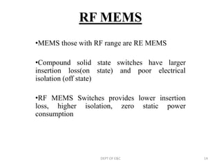
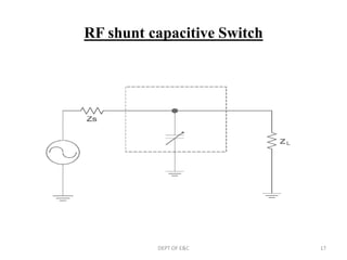
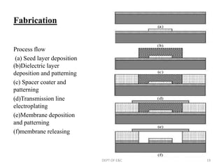
This document discusses Micro-Electro-Mechanical Systems (MEMS) technology. It begins with an introduction to MEMS and differences between MEMS and integrated circuits. It then describes basic MEMS elements and the manufacturing processes, including photolithography, micromachining, and laser micromachining. RF MEMS switches are discussed next, including series contact and shunt capacitive switches. Fabrication processes and comparisons with solid state switches are provided. Applications of MEMS in various fields are mentioned. The document concludes that MEMS switches are an alternative to solid state switches due to their low power consumption and high isolation.