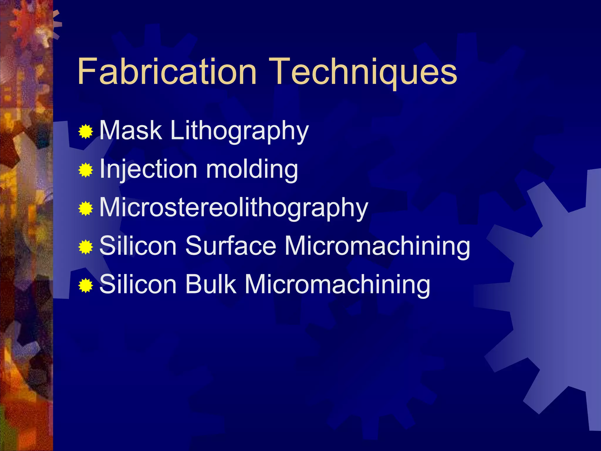
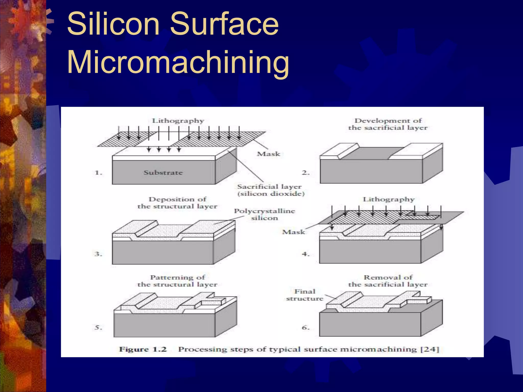
MEMS Fabrication
Mr.S.S.Gurav
SITCOE
MEMS overview
 Micron level mechanical parts
 Made from transistor materials and
metals
Fabrication Techniques
 Mask Lithography
 Injection molding
 Microstereolithography
 Silicon Surface Micromachining
 Silicon Bulk Micromachining
Mask Lithography
 Use of photo resist
 Positive
 Dissolves under light
 Negative
 Hardens under light
 Both get covered with desired material,
then photo resist is dissolved by a solvent
 Multiple layers – Multiple steps
Mask Lithography
Injection Molding
 Starts with mask lithography
 Metal poured over resist
 Resist gets dissolved
 Metal form is left for plastic injection
molding
Injection Molding
Microstereolithography
 Similar principal to mask lithography, but for 3D pieces
 Uses an “active mask”
 Not a physical mask
 Utilizes a photo-reactive acrylic resin
 Each layer image projected through a DMD(digital mirror device)
 Projected into the resin
 Uses lenses
 Resin that is illuminated, Cross-links and hardens
 Piece is then covered in a hardened layer
Microstereolithography
 Dimensional capabilities
Lateral and Vertical resolution: 10μm
Maximum field size: 10.24mm x
7.68mm
Structural height: up to 5mm
Microstereolithography
Silicon Surface
Micromachining
 Uses the same process as IC fabrication
 Needs multiple layers to create structures
 Cheapest form of Micromachining
 Similar to lithography
 Sacrificial material
 Structural material
 When sacrificial material is removed, only
whole structures are left
Silicon Surface
Micromachining
Silicon Surface
Micromachining
Silicon Surface
Micromachining
Silicon Bulk Micromachining
 Done with Crystalline silicon
 Constructed using etch stop planes
 Chemical process
 Anisotropic Etching
 Speed dependent – Directional
 etch in different crystallographic directions at
different rates
 Slower directions create and etch stop plane
Deep Reactive Ion Etching (DRIE)
 Uses photo resist
and a mask to
create structures
Sapphire Etching
 Metal Mask
 100µm etch depth
 .28µm/min etch rate
 Chlorine etching
Pressure Sensor Etching
 Used on silicon
 Metal mask
 .81µm etch depth
 Utilizes Fluorine
High-Speed Etching
 Silicon material
 1µm/min etch rate
 Si Mask

Mems fabrication