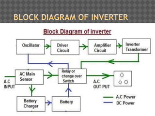
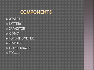
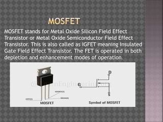
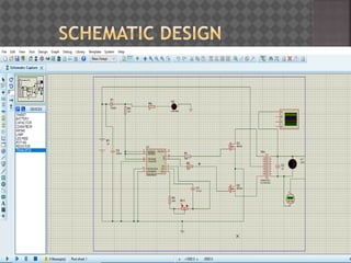
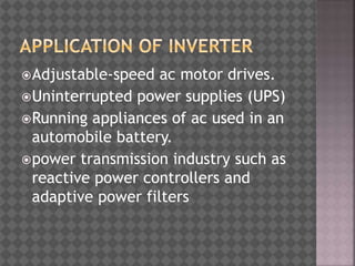
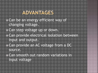
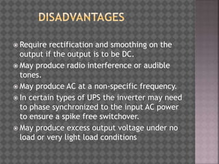
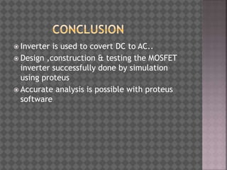
PRESENTED BY
MOHAMMAD HANNAN(21304014)
UNDER THE GUIDANCE OF
PROF. DR. K. ANUSUDHA
M.TECH IN ELCTRONICS AND COMMUNICATION ENGG.
DEPARTMENT OF ELECTRONICS ENGINEERING
SCHOOL OF ENGINEERING AND TECHNOLOGY
PONDICHERRY UNIVERSITY
PONDICHERRY(605014)
 INVERTER
 WORKING
 BLOCK DIAGRAM
 DESCRIPTIONS &WORKING OF COMPONENTS
 SCHEMATIC DESIGN
 OUTPUT
 APPLICATIONS
 ADVANTAGES & DISADVANTAGES
 CONCLUSION
A device that converts direct current
electricity to alternating current either for
stand-alone systems or to supply power to an
electricity grid
 The working of an inverter is, it converts DC
to AC, and these devices never generate any
kind of power because the power is
generated by the DC source. In some
situations like when the DC voltage is low
then we cannot use the low DC voltage in a
home appliance. So due to this reason, an
inverter can be used whenever we utilize
solar power panel
 MOSFET
 BATTERY
 CAPACITOR
 IC4047
 POTENTIOMETER
 RESISTOR
 TRANSFORMER
 ETC……..
The MOSFET is a three-terminal (gate, drain, and source)
fully-controlled switch. The gate/control signal occurs
between the gate and source, and its switch terminals are
the drain and source. The gate itself is made of metal,
separated from the source and drain using a metal oxide.
This allows for less power consumption, and makes the
transistor a great choice for use as an electronic switch or
common-source amplifier.
In order to function properly, MOSFETs have to maintain a
positive temperature coefficient. This means there’s little-
to-no chance of thermal runaway. On-state losses are
lower because the transistor’s on-state-resistance,
theoretically speaking, has no limit. Also, because
MOSFETs can operate at high frequencies, they can
perform fast switching applications with little turn-off
losses.
MOSFET stands for Metal Oxide Silicon Field Effect
Transistor or Metal Oxide Semiconductor Field Effect
Transistor. This is also called as IGFET meaning Insulated
Gate Field Effect Transistor. The FET is operated in both
depletion and enhancement modes of operation.
 Improved switching speeds
 Improved dynamic performance that requires
even less power from the driver.
 Lower gate-to-drain feedback capacitance
 Lower thermal impedance which, in turn,
has enabled much better power dissipation.
 Lower rise and fall times, which has allowed
for operation at higher switching
frequencies.
 MOSFET is a low cost
A battery is a device in which we can use the energy as a
source of power. The energy which store in battery is in
the form of chemical energy which is converted into
electrical energy. In this circuit we are using 12 volt
battery for simulate our circuit
A capacitor is a component which has a ability to stores the
energy in it. The store energy is in the form of electrical
charges..
There are 14 pins available on the IC where Vss stand for
ground pin and Vdd is voltage supply pin. There are six
inputs including, trigger, astable, external reset and
retrigger.
A potentiometer is a three-terminal resistor in which the
resistance can control the flow of electric current. In
short we can say that it’s easily to control the flow of
electron
A resistor is a two-terminal electrical component which is
used in a circuit element. Resistors are used to reduce
the flow of current and also adjust the signal levels
A transformer is a device which flow the electric energy
from one terminal to another terminal. We can say that it
can reduce or increase the voltage of an AC
CD 4047 is a low power CMOS astable/monostable
multivibrator IC. Here it is wired as an astable
multivibrator producing two pulse trains of 0.01s
which are 180 degrees out of phase at the pins 10
and 11 of the IC. Pin 10 is connected to the gate
of Q1 and pin 11 is connected to the gate of Q2.
Resistors R3 and R4 prevents the loading of the IC
by the respective MOSFETs. When pin 10 is high
Q1 conducts and current flows through the upper
half of the transformer primary which accounts
for the positive half of the output AC voltage.
When pin 11 is high Q2 conducts and current
flows through the lower half of the transformer
primary in opposite direction and it accounts for
the negative half of the output AC voltage
Adjustable-speed ac motor drives.
Uninterrupted power supplies (UPS)
Running appliances of ac used in an
automobile battery.
power transmission industry such as
reactive power controllers and
adaptive power filters
 Can be an energy efficient way of
changing voltage.
 Can step voltage up or down.
 Can provide electrical isolation between
input and output.
 Can provide an AC voltage from a DC
source.
 Can smooth out random variations in
input voltage
 Require rectification and smoothing on the
output if the output is to be DC.
 May produce radio interference or audible
tones.
 May produce AC at a non-specific frequency.
 In certain types of UPS the inverter may need
to phase synchronized to the input AC power
to ensure a spike free switchover.
 May produce excess output voltage under no
load or very light load conditions
 Inverter is used to covert DC to AC..
 Design ,construction & testing the MOSFET
inverter successfully done by simulation
using proteus
 Accurate analysis is possible with proteus
software
1) “Mgottlieb, I. (1985). Power switching Regulator
Inverters and Converters (1st Edition). Tab Book Inc.’’
2) “Theraja, B.L. and Theraja, A.K. (1999). Textbook of
Electrical Technology. (Twenty-Second Edition).
Prentice Hall Inc.”
3) “Lander, C.W. (1999). Power Electronics (Second
Edition). S Chad & Company.
4) ”Hill, W and Horowitz, P (1995) Art of Electronic,
2nd Edition, Great Britain, Cambridge”
5) “K. Phillips, (2000) “Power Electronics: Will Our
Current Technical Vision Take Us to The Next Level of
A.C Drive Product Performance?” in Rec. 2000 IEEE
Appl. Conf., Rome, Italy, Oct. 2000, pp. P-1–P-9
MOSFET INVERTER SIMULATION

MOSFET INVERTER SIMULATION

  • 2.
    PRESENTED BY MOHAMMAD HANNAN(21304014) UNDERTHE GUIDANCE OF PROF. DR. K. ANUSUDHA M.TECH IN ELCTRONICS AND COMMUNICATION ENGG. DEPARTMENT OF ELECTRONICS ENGINEERING SCHOOL OF ENGINEERING AND TECHNOLOGY PONDICHERRY UNIVERSITY PONDICHERRY(605014)
  • 3.
     INVERTER  WORKING BLOCK DIAGRAM  DESCRIPTIONS &WORKING OF COMPONENTS  SCHEMATIC DESIGN  OUTPUT  APPLICATIONS  ADVANTAGES & DISADVANTAGES  CONCLUSION
  • 4.
    A device thatconverts direct current electricity to alternating current either for stand-alone systems or to supply power to an electricity grid
  • 5.
     The workingof an inverter is, it converts DC to AC, and these devices never generate any kind of power because the power is generated by the DC source. In some situations like when the DC voltage is low then we cannot use the low DC voltage in a home appliance. So due to this reason, an inverter can be used whenever we utilize solar power panel
  • 7.
     MOSFET  BATTERY CAPACITOR  IC4047  POTENTIOMETER  RESISTOR  TRANSFORMER  ETC……..
  • 8.
    The MOSFET isa three-terminal (gate, drain, and source) fully-controlled switch. The gate/control signal occurs between the gate and source, and its switch terminals are the drain and source. The gate itself is made of metal, separated from the source and drain using a metal oxide. This allows for less power consumption, and makes the transistor a great choice for use as an electronic switch or common-source amplifier. In order to function properly, MOSFETs have to maintain a positive temperature coefficient. This means there’s little- to-no chance of thermal runaway. On-state losses are lower because the transistor’s on-state-resistance, theoretically speaking, has no limit. Also, because MOSFETs can operate at high frequencies, they can perform fast switching applications with little turn-off losses.
  • 9.
    MOSFET stands forMetal Oxide Silicon Field Effect Transistor or Metal Oxide Semiconductor Field Effect Transistor. This is also called as IGFET meaning Insulated Gate Field Effect Transistor. The FET is operated in both depletion and enhancement modes of operation.
  • 10.
     Improved switchingspeeds  Improved dynamic performance that requires even less power from the driver.  Lower gate-to-drain feedback capacitance  Lower thermal impedance which, in turn, has enabled much better power dissipation.  Lower rise and fall times, which has allowed for operation at higher switching frequencies.  MOSFET is a low cost
  • 11.
    A battery isa device in which we can use the energy as a source of power. The energy which store in battery is in the form of chemical energy which is converted into electrical energy. In this circuit we are using 12 volt battery for simulate our circuit
  • 12.
    A capacitor isa component which has a ability to stores the energy in it. The store energy is in the form of electrical charges..
  • 13.
    There are 14pins available on the IC where Vss stand for ground pin and Vdd is voltage supply pin. There are six inputs including, trigger, astable, external reset and retrigger.
  • 14.
    A potentiometer isa three-terminal resistor in which the resistance can control the flow of electric current. In short we can say that it’s easily to control the flow of electron
  • 15.
    A resistor isa two-terminal electrical component which is used in a circuit element. Resistors are used to reduce the flow of current and also adjust the signal levels
  • 16.
    A transformer isa device which flow the electric energy from one terminal to another terminal. We can say that it can reduce or increase the voltage of an AC
  • 18.
    CD 4047 isa low power CMOS astable/monostable multivibrator IC. Here it is wired as an astable multivibrator producing two pulse trains of 0.01s which are 180 degrees out of phase at the pins 10 and 11 of the IC. Pin 10 is connected to the gate of Q1 and pin 11 is connected to the gate of Q2. Resistors R3 and R4 prevents the loading of the IC by the respective MOSFETs. When pin 10 is high Q1 conducts and current flows through the upper half of the transformer primary which accounts for the positive half of the output AC voltage. When pin 11 is high Q2 conducts and current flows through the lower half of the transformer primary in opposite direction and it accounts for the negative half of the output AC voltage
  • 20.
    Adjustable-speed ac motordrives. Uninterrupted power supplies (UPS) Running appliances of ac used in an automobile battery. power transmission industry such as reactive power controllers and adaptive power filters
  • 21.
     Can bean energy efficient way of changing voltage.  Can step voltage up or down.  Can provide electrical isolation between input and output.  Can provide an AC voltage from a DC source.  Can smooth out random variations in input voltage
  • 22.
     Require rectificationand smoothing on the output if the output is to be DC.  May produce radio interference or audible tones.  May produce AC at a non-specific frequency.  In certain types of UPS the inverter may need to phase synchronized to the input AC power to ensure a spike free switchover.  May produce excess output voltage under no load or very light load conditions
  • 23.
     Inverter isused to covert DC to AC..  Design ,construction & testing the MOSFET inverter successfully done by simulation using proteus  Accurate analysis is possible with proteus software
  • 24.
    1) “Mgottlieb, I.(1985). Power switching Regulator Inverters and Converters (1st Edition). Tab Book Inc.’’ 2) “Theraja, B.L. and Theraja, A.K. (1999). Textbook of Electrical Technology. (Twenty-Second Edition). Prentice Hall Inc.” 3) “Lander, C.W. (1999). Power Electronics (Second Edition). S Chad & Company. 4) ”Hill, W and Horowitz, P (1995) Art of Electronic, 2nd Edition, Great Britain, Cambridge” 5) “K. Phillips, (2000) “Power Electronics: Will Our Current Technical Vision Take Us to The Next Level of A.C Drive Product Performance?” in Rec. 2000 IEEE Appl. Conf., Rome, Italy, Oct. 2000, pp. P-1–P-9