More Related Content Similar to Lect2 up110 (100324) Similar to Lect2 up110 (100324) (20) 1. Lecture 110 – Linear Circuit Models (3/24/10) Page 110-1
LECTURE 110 – LINEAR CIRCUIT MODELS
LECTURE ORGANIZATION
Outline
• Frequency independent small signal transistor models
• Frequency dependent small signal transistor model
• Noise models
• Passive component models
• Interconnects
• Substrate interference
• Summary
CMOS Analog Circuit Design, 2nd Edition Reference
Pages 86-91 and new material
CMOS Analog Circuit Design © P.E. Allen - 2010
Lecture 110 – Linear Circuit Models (3/24/10) Page 110-2
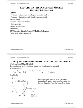
FREQUENCY INDEPENDENT SMALL SIGNAL TRANSISTOR MODELS
What is a Small Signal Model?
The small signal model is a linear approximation of a nonlinear model.
Mathematically:
iD =
2
Large Signal to Small Signal
(vGS - VT)2 id = gmvgs
Graphically:
The large signal curve at point Q has been
approximated with a small signal model going
through the point Q and having a slope of gm.
id = gmvgs
id
Q
vgs
v V GS GS
060311-03
iD = β(vGS-VT)2
iD
ID
VT
CMOS Analog Circuit Design © P.E. Allen - 2010
2. Lecture 110 – Linear Circuit Models (3/24/10) Page 110-3
Why Small Signal Models?
The small signal model is a linear approximation to the large signal behavior.
1.) The transistor is biased at given DC operating point (Point Q above)
2.) Voltage changes are made about the operating point.
3.) Current changes result from the voltage changes.
If the designer is interested in only the current changes and not the DC value, then the
small signal model is a fast and simple way to find the current changes given the voltage
changes.
Large Signal
Model
id = gmvgs
vgs
060311-04
ΔiDʼ
id
Q
ΔVGS
ΔiD
CMOS Analog Circuit Design © P.E. Allen - 2010
Lecture 110 – Linear Circuit Models (3/24/10) Page 110-4
How Good is the Small Signal Model?
It depends on how large are the changes and how nonlinear is the large signal model.
• The parameters of the small signal model will depend on the values of the large signal
model.
• The model is a tradeoff in complexity versus accuracy (we will choose simplicity and
give up accuracy).
• What does a simulator do? Exactly the same thing when it makes an ac analysis (i.e.
frequency response)
• Regardless of the approximate nature of the small signal model, it is the primary model
used to predict the signal performance of an analog circuit.
CMOS Analog Circuit Design © P.E. Allen - 2010
3. Lecture 110 – Linear Circuit Models (3/24/10) Page 110-5
Small-Signal Model for the Saturation Region
The small-signal model is a linearization of the large signal model about a quiescent or
operating point.
Consider the large-signal MOSFET in the saturation region (vDS vGS – VT) :
iD =
WμoCox
2L (vGS - VT) 2 (1 + vDS)
The small-signal model is the linear dependence of id on vgs, vbs, and vds. Written as,
id gmvgs + gmbsvbs + gds vds
where
gm
diD
dvGS |Q
= (VGS-VT) = 2ID
gds
diD
dvDS |Q
=
ID
1+VDS ID
and
gmbs
dD
dvBS
|Q
=
diD
dvGS
6. |Q
=
gm
2 2| F|-VBS
= gm
CMOS Analog Circuit Design © P.E. Allen - 2010
Lecture 110 – Linear Circuit Models (3/24/10) Page 110-6
Small-Signal Model – Continued
Complete schematic
model:
where
gm
diD
dvGS |Q
=
G
D
S
B
(VGS-VT) = 2ID gds
G
D
S
diD
dvDS |Q
B
=
G
+
vgs
S
-
B
+
vbs
-
iD
1+vDS iD
and
gmbs =
D
vBS
iD
vGS
|Q =
9. |Q
=
gmvgs
gm
gmbsvbs
2 2| F|-VBS
= gm
Simplified schematic model:
A very useful assumption:
gm 10gmbs 100gds
rds
id
+
D
vds
-
S
Fig. 120-0
CMOS Analog Circuit Design © P.E. Allen - 2010
10. Lecture 110 – Linear Circuit Models (3/24/10) Page 110-7
Small-Signal Model for other Regions
Active region:
gm =
iD
vGS
|Q
=
K’WVDS
L (1+VDS)
K’W
L VDS gmbs =
iD
vBS
|Q
=
K’WVDS
2L 2F-VBS
gds =
iD
vDS
|Q
=
K’W
L ( VGS - VT - VDS)(1+VDS) +
ID
1+VDS
K’W
L (VGS - VT - VDS)
Note:
While the small-signal model analysis is independent of the region of operation, the
evaluation of the small-signal performance is not.
Weak inversion region:
If vDS 0, then
iD = It
WL
exp
vGS-VT
nVt
vDS
VA
1+
Small-signal model:
gm =
diD
dvGS |Q
= It
WL
It
nVt exp
vGS-VT
nVt
vDS
VA =
1+
ID
nVt =
qID
nkT =
ID
Vt
Cox
Cox+Cjs
gds =
diD
dvDS |Q
ID
VA
CMOS Analog Circuit Design © P.E. Allen - 2010
Lecture 110 – Linear Circuit Models (3/24/10) Page 110-8
FREQUENCY DEPENDENT SMALL SIGNAL MODEL
Small-Signal Frequency Dependent Model
The depletion capacitors are found by evaluating the large signal capacitors at the DC
operating point.
The charge storage capacitors are constant for a specific region of operation.
CMOS Analog Circuit Design © P.E. Allen - 2010
11. Lecture 110 – Linear Circuit Models (3/24/10) Page 110-9
Gain-bandwidth of the MOSFET (fT)
The short-circuit current gain is measure of the frequency capability of the MOSFET.
Small signal model:
Small signal analysis
gives,
iout = gmvgs –
sCgdvgs and vgs =
iin
iin
s(Cgs+Cgd)
Therefore,
iout
iin =
gm-sCgd
s(Cgs+Cgd)
gm
iout
s(Cgs+Cgd)
VDD
Assume VSB = 0 and the MOSFET is in saturation,
fT =
1
2
gm
Cgs+Cgd
1
2
gm
Cgs
Recalling that
Cgs
23
WL
CoxWL and gm = μoCox
iin
+
vgs
−
Cgd
Cgs
gmvgs
(VGS-VT) fT =
3
4
iout
rds
060311-05
Cbd
μo
L2 (VGS-VT)
For velocity saturation, fT 1/L.
CMOS Analog Circuit Design © P.E. Allen - 2010
Lecture 110 – Linear Circuit Models (3/24/10) Page 110-10
NOISE MODELS
Derivation of the Thermal Noise Model
The noise model for the MOSFET is developed for the active region as follows:
In the active region, the channel resistance of the MOSFET is given from the simple large
signal model as,
Rchannel =
1
iD
vDS
|Q
=
1
K’W
L (VGS-VT-VDS)
1
K’W
L (VGS-VT)
=
1
gm(sat)
In the saturation region, approximate the channel resistance as 2/3 the value in the active
region giving,
Rchannel(sat) =
2
3gm(sat) =
2
3gm
We know the current thermal noise spectral density of a resistor of value R is given as
in
2 =
4kT
R (A2/Hz)
Substituting R by Rchannel(sat) gives the drain current MOSFET thermal noise model as,
in
2 =
8kTgm
3 (A2/Hz)
Translating this drain current noise to the gate voltage noise by dividing by gm
2 gives
en
2 =
8kT
3gm (V2/Hz)
CMOS Analog Circuit Design © P.E. Allen - 2010
12. Lecture 110 – Linear Circuit Models (3/24/10) Page 110-11
The Influence of the Back Gate on Thermal Noise
Using the derivation above, we can include the influence of the bulk-source voltage on the
thermal noise as follows
Rchannel(sat) =
2
3gm(eff) =
2
3(gm+gmbs) =
2
3gm(1+)
where
=
gmbs
gm
Substituting R with Rchannel(sat) gives the voltage and current noise spectral densities as,
2 =
en
8kT
3(gm+gmbs) (V2/Hz) =
8kT
3gm(1+) (V2/Hz)
or
2 =
in
8kT(gm+gmbs)
3 (A2/Hz) =
8kTgm(1+)
3 (A2/Hz)
CMOS Analog Circuit Design © P.E. Allen - 2010
Lecture 110 – Linear Circuit Models (3/24/10) Page 110-12
1/f Noise Model
Another significant noise contribution to MOSFETs is a noise that is typically inversely
proportional to frequency called the 1/f noise.
This 1/f noise spectral density is given as,
2 =
en
KF
2 =
2fSCoxWLK’ or in
KFID
fSCoxL2
where
KF = Flicker noise coefficient
S = Slope factor of the 1/f noise
Although we do not have a good explanation for the reason why, the value of KF for a
PMOS transistor is smaller than the value of KF for a NMOS transistor with the same
current and W/L. The current will also influence the comparative 1/f noise of the NMOS
and PMOS.
CMOS Analog Circuit Design © P.E. Allen - 2010
13. Lecture 110 – Linear Circuit Models (3/24/10) Page 110-13
MOS Device Noise at Low Frequencies
D
B
S
G
D
S
in2
B
G
Noise
Free
MOSFET
D
eN2
*
G B
S
Noise
Free
MOSFET
where
2 =
in
KFID
fSCoxL2 (amperes2/Hz)
8kTgm(1+)
3 +
=
gmbs
gm
k = Boltzmann’s constant
KF = Flicker noise coefficient
S = Slope factor of the 1/f noise
CMOS Analog Circuit Design © P.E. Allen - 2010
Lecture 110 – Linear Circuit Models (3/24/10) Page 110-14
Reflecting the MOSFET Noise to the Gate
Dividing i2 by gn
m
2 gives the voltage noise spectral density as
2 =
en
in
2
gm
2 =
8kT
3gm(1+)+
KF
2fCoxWLK’ (volts2/Hz)
It will be convenient to use B =
KF
2CoxK’ to simplify the notation.
Frequency response of MOSFET noise:
1/f noise
Thermal noise
f log10 f Corner
060311-06
Noise Spectral
Density
The 1/f corner frequency is:
8kT
3gm(1+) =
KF
2fCoxWLK’ fcorner
3gmB
8kTWL if gmbs = 0
CMOS Analog Circuit Design © P.E. Allen - 2010
14. Lecture 110 – Linear Circuit Models (3/24/10) Page 110-15
MOSFET Noise Model at High Frequencies
At high frequencies, the source resistance can no longer be assumed to be small.
Therefore, a noise current generator at the input results.
MOSFET Noise Models:
Cgd
G D
vgs
vin rds in2 io2
gmvgs
Cgs
S S
Circuit 1: Frequency Dependent Noise Model
Cgd
ei2
G D
vgs
*
vin ii2 rds io2
gmvgs
Cgs
S S
Circuit 2: Input-referenced Noise Model
CMOS Analog Circuit Design © P.E. Allen - 2010
Lecture 110 – Linear Circuit Models (3/24/10) Page 110-16
MOSFET Noise Model at High Frequencies – Continued
To find e2 and ii
i
2, we will perform the following calculations:
2:
Short-circuit the input and find io
ei
2 of both models and equate to get ei
2 .
Ckt. 1: io
2 = in
2
Ckt. 2: io
2 = gm
2+ (Cgd)2ei
2 ei
2
i2:
i
Open-circuit the input and find io
2=
ei
in
2
gm
2+(Cgd)2
2 of both models and equate to get ii
2 .
Ckt. 1: io
2 = in
2
2 =
Ckt. 2: io
16. (1/Cgs)
(1/Cds)+(1/Cgs) 2 ii
2 +
gm
2ii
2
2(Cgs+Cds)2
gm
2
2 if Cgd Cgs ii
2 in
2Cgs
2 =
2Cgs
2
gm
2 in
2
CMOS Analog Circuit Design © P.E. Allen - 2010
17. Lecture 110 – Linear Circuit Models (3/24/10) Page 110-17
PASSIVE COMPONENT MODELS
Resistor Models
1.) Large signal
2.) Small signal
v = Ri
3.) Noise
en
v
R(v)
+ −
i
Cp
Distributed Model Lumped Model
i
2 = 4kTR or in
i
Cp1 Cp2
Conductivity
modulation
v
i = vR
060311-01
2 = 4kTG
v
+ −
060315-01
R(v)
CMOS Analog Circuit Design © P.E. Allen - 2010
Lecture 110 – Linear Circuit Models (3/24/10) Page 110-18
Capacitor Models
1.) Large signal
2.) Small signal
+ −
v
i
Cp Cp
C
q = Cv i = C(dv/dt)
060315-03
Rp
C(v)
v
Nonlinear
060315-04
Linear
3.) Do capacitors have noise? See next page.
One of the parasitic capacitors
is the top plate and the other
is associated with the bottom
plate.
CMOS Analog Circuit Design © P.E. Allen - 2010
18. Lecture 110 – Linear Circuit Models (3/24/10) Page 110-19
Switched Capacitor Circuits - kT/C Noise
Capacitors and switches generate an inherent thermal noise given by kT/C. This noise is
verified as follows.
An equivalent circuit for a switched
Ron
capacitor:
vin C vout vin C vout
060315-05
The noise voltage spectral density of switched capacitor above is given as
e 2
Ron = 4kTRon Volts2/Hz =
2kTRon
Volt2/Rad./sec.
The rms noise voltage is found by integrating this spectral density from 0 to to give
v 2
Ron =
2kTRon
1
0
2d
1
2+2 =
2kTRon
1
2 =
20. kT
C Volts(rms)2
where 1 = 1/(RonC). Note that the switch has an effective noise bandwidth of
fsw =
1
4RonC Hz
which is found by dividing the second relationship by the first.
CMOS Analog Circuit Design © P.E. Allen - 2010
Lecture 110 – Linear Circuit Models (3/24/10) Page 110-20
Inductor Models
R = losses of the inductor
Cp = parasitic capacitance to ground
Rp = losses due to eddy currents caused by magnetic flux
1.) Large Signal
2.) Small signal
= Li
L
i
Linear
Nonlinear
d
dt = v = L
di
dt
3.) Mutual inductance
di1
dt + M
v1 = L1
di2
dt
v2 = M
di1
dt + L2
di2
dt
060316-04
i1 i2
+
v2
−
L2-M
060316-05
+
v1
−
i1 i2
+
v2
−
+
v1
−
L1-M
M
L1 L2
M
k =
M
L1L2
CMOS Analog Circuit Design © P.E. Allen - 2010
21. Lecture 110 – Linear Circuit Models (3/24/10) Page 110-21
INTERCONNECTS
Types of “Wires”
1.) Metal
Many layers are available in today’s technologies:
- Lower level metals have more resistance (70 m/sq.)
- Upper level metal has the less resistance because it is thicker (50 m/sq.)
2.) Polysilicon
Better resistor than conductor (unpolysicided) (135/sq.)
Silicided polysilicon has a lower resistance (5/sq.)
3.) Diffusion
Reasonable for connections if silicided (5/sq.)
Unsilicided (55/sq.)
4.) Vias
Vias are vertical metal (tungsten plugs or aluminum)
- Connect metal layer to metal layer (3.5/via)
- Connect metal to silicon or polysilicon contact resistance (5/contact)
CMOS Analog Circuit Design © P.E. Allen - 2010
Lecture 110 – Linear Circuit Models (3/24/10) Page 110-22
Ohmic Contact Resistance
The metal to silicon contact generates resistance because of the presence of a potential
barrier between the metal and the silicon.
Contact and Via Resistance:
Contact System
Contact
Resistance
(/μm2)
Al-Cu-Si to 160/sq. base 750
Al-Cu-Si to 5/sq. emitter 40
Al-Cu/Ti-W/PtSi to
160/sq. base
1250
Al-Cu/Al-Cu (Via) 5
Al-Cu/Ti-W/Al-Cu (Via) 5
050319-02
Metal 1
Metal 3
Metal 2
Aluminum
Vias
Tungsten
Plugs
Transistors
CMOS Analog Circuit Design © P.E. Allen - 2010
22. Lecture 110 – Linear Circuit Models (3/24/10) Page 110-23
Capacitance of Wires
Self, fringing and coupling capacitances:
Wide Spacing Minimum Spacing
CCoupling
CFringe
CSelf
CCoupling
CFringe
Ground plane
050319-03
Capacitance Typical Value Units
Metal to diffusion, Self capacitance 33 aF/μm2
Metal to diffusion, Fringe capacitance, minimum spacing 7 aF/μm
Metal to diffusion, Fringe capacitance, wide spacing 40 aF/μm
Metal to metal, Coupling capacitance, minimum spacing 85 aF/μm
Metal to substrate, Self capacitance 28 aF/μm2
Metal to substrate, Fringe capacitance, minimum spacing 4 aF/μm
Metal to substrate, Fringe capacitance, wide spacing 39 aF/μm
CMOS Analog Circuit Design © P.E. Allen - 2010
Lecture 110 – Linear Circuit Models (3/24/10) Page 110-24
Electromigration
Electromigration occurs if the current density is too large and the pressure of carrier
collisions on the metal atoms causes a slow displacement of the metal.
Black’s law:
MTF =
1
AJ2 e(Ea/kTj)
Where
Metal 050304-04
A = rate constant (cm4/A2/hr)
J = current density (A/cm2)
Ea = activation energy in electron volts (0.5eV for Al and 0.7eV for Cu doped Al)
k = Boltzmann’s constant (8.6x10⁻⁵ eV/K)
Electromigration leads to a maximum current density,Jmax. Jmax for copper doped
aluminum is 5x10⁵ A/cm2 at 85°C.
If t = 10,000 Angstroms and Jmax = 5x10⁵ A/cm2, then a 10μm wide lead can conduct no
more than 50mA at 85°C.
CMOS Analog Circuit Design © P.E. Allen - 2010
23. Lecture 110 – Linear Circuit Models (3/24/10) Page 110-25
Where is AC Ground on the Chip?
AC grounds on the chip are any area tied to a fixed potential. This includes the substrate
and the wells. All parasitic capacitances are in reference to these points.
Protective Insulator Layer
VDD GRD
Metal Vias Metal Via
Tungsten Plugs
Sidewall
Spacers Polycide
Salicide Salicide Salicide
n+ p+
p+ p+ n+ n+
Shallow
Trench
Isolation
AC Ground DC and AC Ground
n-well p-well
Tungsten
Plug
Shallow
Trench
Isolation
Substrate
GRD
p+
Tungsten
Plugs
Tungsten
Plugs
Shallow
Trench
Isolation
DC Ground
Oxide p+ p p- n- n n+ Salicide Metal
Poly
Top
Metal
Second
Level
Metal
First
Level
Metal
Inter-mediate
Oxide
Layers
060405-05
Polycide
Salicide
Gate Ox
CMOS Analog Circuit Design © P.E. Allen - 2010
Lecture 110 – Linear Circuit Models (3/24/10) Page 110-26
Grounds that are Not Grounds
Because of the resistance of “wires”, current flowing through a wire can cause a voltage
drop.
An example of good and bad
practice: Circuit
A
Bad:
Circuit
B
Circuit
C
R R R
IA IA+IB IA+IB+IC
Better:
Circuit
A
Circuit
B
IA
Circuit
C
IB
IC
3R
2R
R
Best:
Circuit
A
R
Circuit
B
Circuit
C
IA R IB R IC
050305-04
CMOS Analog Circuit Design © P.E. Allen - 2010
24. Lecture 110 – Linear Circuit Models (3/24/10) Page 110-27
Kelvin Connections
Avoid unnecessary ohmic drops.
A B A B
X Y
Ohmic Connection Kelvin Connection 041223-12
In the left-hand connection, an IR drop is experienced between X and Y causing the
potentials at A and B to be slightly different.
For example, let the current be 100μA and the metal be 30m/sq. Suppose that the
distance between X and Y is 100 squares. Therefore, the IR drop is
100μA x 30m/sq. x 100sq. = 0.3mV
CMOS Analog Circuit Design © P.E. Allen - 2010
Lecture 110 – Linear Circuit Models (3/24/10) Page 110-28
SUBSTRATE NOISE INTERFERENCE
Methods of Substrate Injection
• Hot carrier
• Leakage
• Minority Carrier
• Displacement Current (large devices)
CMOS Analog Circuit Design © P.E. Allen - 2010
25. Lecture 110 – Linear Circuit Models (3/24/10) Page 110-29
Other Methods of Substrate Injection
CMOS Analog Circuit Design © P.E. Allen - 2010
Lecture 110 – Linear Circuit Models (3/24/10) Page 110-30
Illustration of Noise Interference Mechanism – No Epi
CMOS Analog Circuit Design © P.E. Allen - 2010
26. Lecture 110 – Linear Circuit Models (3/24/10) Page 110-31
Illustration of Noise Interference Mechanism – With Epi
CMOS Analog Circuit Design © P.E. Allen - 2010
Lecture 110 – Linear Circuit Models (3/24/10) Page 110-32
How is Noise Injected into Components?
MOSFETs:
Injection occurs by the bulk effect on the
threshold and across the depletion
capacitance.
BJTs:
Injection primarily across the depletion
capacitance.
Passives:
CMOS Analog Circuit Design © P.E. Allen - 2010
27. ISOLATION TECHNIQUES
Lecture 110 – Linear Circuit Models (3/24/10) Page 110-33
Isolation Techniques
Isolation techniques include both layout and circuit approaches to isolating quiet from
noisy circuits.
CMOS Analog Circuit Design © P.E. Allen - 2010
Lecture 110 – Linear Circuit Models (3/24/10) Page 110-34
Isolation Techniques – Guard Rings
• Collect the majority/minority carriers in the substrate
• Connect the guard rings to external potentials through conductors with
- Minimum resistance
- Minimum inductance v = L
di
dt
CMOS Analog Circuit Design © P.E. Allen - 2010
28. Lecture 110 – Linear Circuit Models (3/24/10) Page 110-35
Isolation Techniques - Layout
Separation:
Physical separation – works well for non-epi, less for epi
Trenches:
Good if filled with a dielectric, not good if filled with a
conductor.
Layout:
Common centroid geometry does
not help.
Keep contact and via resistance to a
minimum.
Wells help to isolate (deep n-well)
CMOS Analog Circuit Design © P.E. Allen - 2010
CIRCUIT TECHNIQUES
Lecture 110 – Linear Circuit Models (3/24/10) Page 110-36
Isolation Techniques - Noise Insensitive Circuit Design
• Design for high power supply rejection ratio (PSRR)
• Correlated sampling techniques – eliminate low frequency noise
• Use “quiet” digital logic (power supply current remains constant)
• Use differential signal processing techniques.
Example of a 4th order Sigma Delta modulator using differential circuits:
CMOS Analog Circuit Design © P.E. Allen - 2010
29. Lecture 110 – Linear Circuit Models (3/24/10) Page 110-37
Noise Isolation Techniques - Reduction of Package Parasitics
• Keep the lead
inductance to a
minimum (multiple
bond wires)
• Package selection
Leadless lead frame: Micro surface mount device:
Still has
bond wires Minimum
inductance
package
CMOS Analog Circuit Design © P.E. Allen - 2010
Lecture 110 – Linear Circuit Models (3/24/10) Page 110-38
Summary of Substrate Interference
• Methods to reduce substrate noise
1.) Physical separation
2.) Guard rings placed close to the sensitive circuits with dedicated package pins.
3.) Reduce the inductance in power supply and ground leads (best method)
4.) Connect regions of constant potential (wells and substrate) to metal with as
many contacts as possible.
• Noise Insensitive Circuit Design Techniques
1.) Design for a high power supply rejection ratio (PSRR)
2.) Use multiple devices spatially distinct and average the signal and noise.
3.) Use “quiet” digital logic (power supply current remains constant)
4.) Use differential signal processing techniques.
• Some references
1.) D.K. Su, M.J. Loinaz, S. Masui and B.A. Wooley, “Experimental Results and Modeling Techniques for
Substrate Noise in Mixed-Signal IC’s,” J. of Solid-State Circuits, vol. 28, No. 4, April 1993, pp. 420-430.
2.) K.M. Fukuda, T. Anbo, T. Tsukada, T. Matsuura and M. Hotta, “Voltage-Comparator-Based
Measurement of Equivalently Sampled Substrate Noise Waveforms in Mixed-Signal ICs,” J. of Solid-State
Circuits, vol. 31, No. 5, May 1996, pp. 726-731.
3.) X. Aragones, J. Gonzalez and A. Rubio, Analysis and Solutions for Switching Noise Coupling in Mixed-
Signal ICs, Kluwer Acadmic Publishers, Boston, MA, 1999.
CMOS Analog Circuit Design © P.E. Allen - 2010
30. Lecture 110 – Linear Circuit Models (3/24/10) Page 110-39
SUMMARY
• Small signal models are a linear representation of the transistor electrical behavior
• Including the transistor capacitors in the small signal model gives frequency dependence
• Noise models include thermal and 1/f noise voltage or current spectral density models
• Passive component models include the nonlinearity, small signal and noise models
• Interconnects include metal, polysilicon, diffusion and vias
• Electromigration occurs if the current density is too large causing a displacement of
metal
• Substrate interference is due to interaction between various parts of an integrated circuit
via the substrate
• Method to reduce substrate interference include:
- Physical separation
- Guard rings
- Reduced inductance in the power supply and ground leads
- Appropriate contacts to the regions of constant potential
- Reduce the source of interfering noise
- Use differential signal processing techniques
CMOS Analog Circuit Design © P.E. Allen - 2010