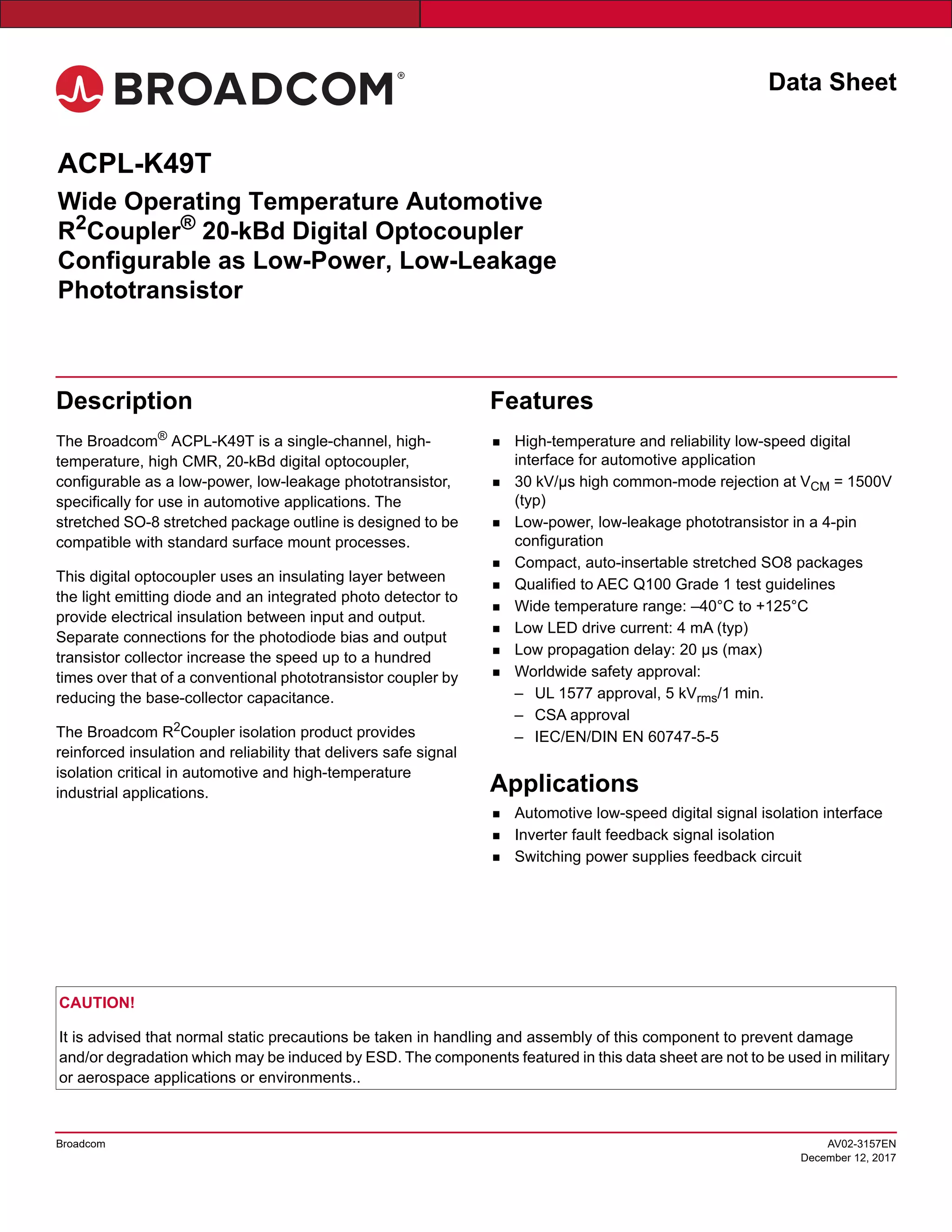
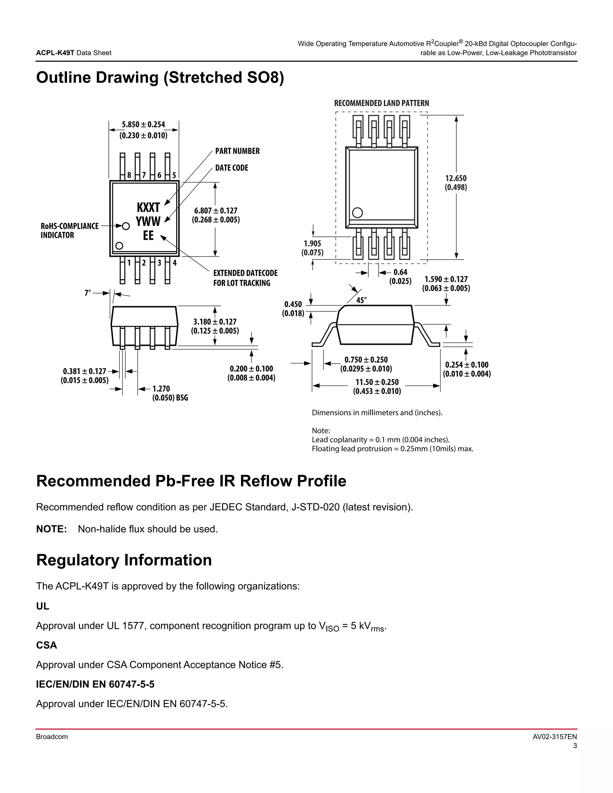
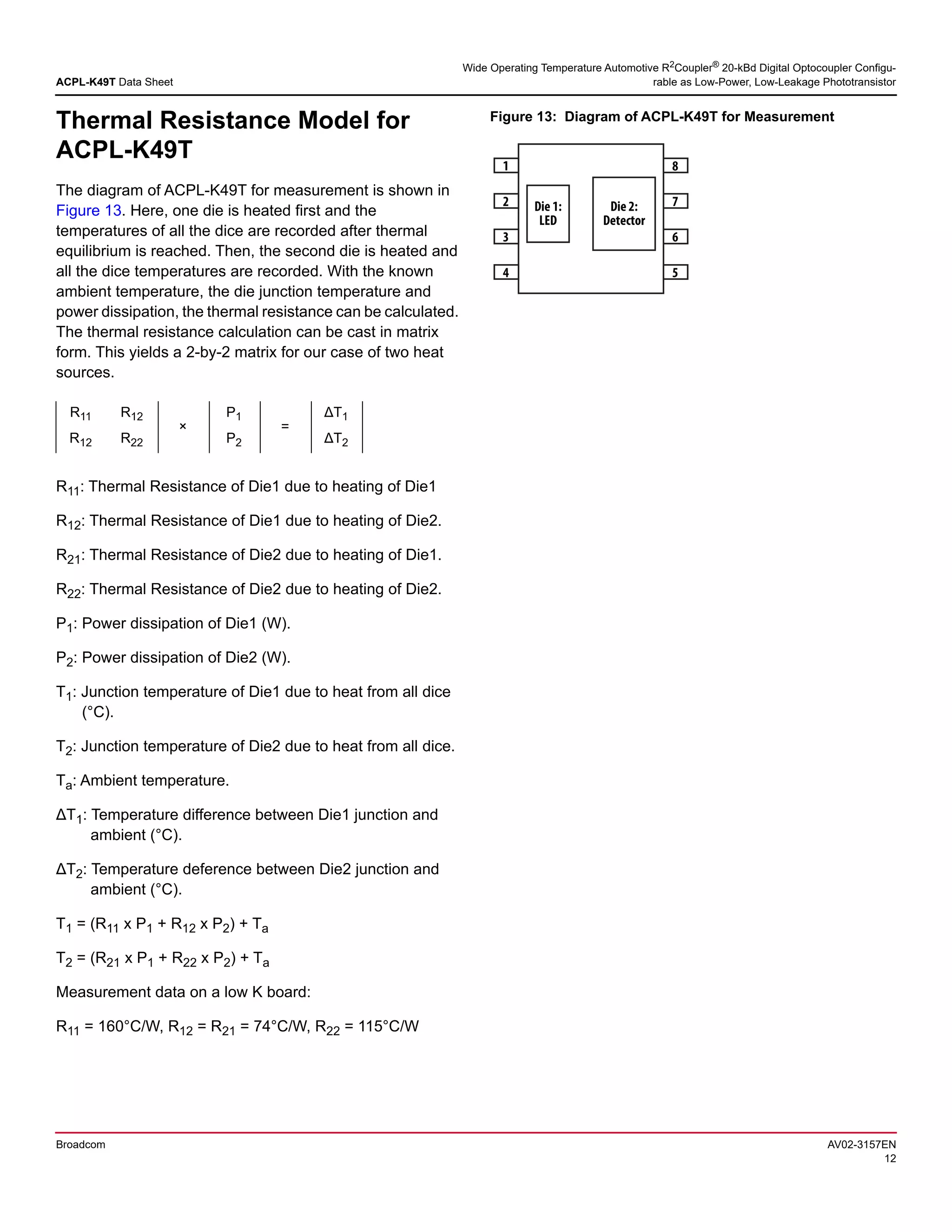
This data sheet provides specifications for the Broadcom ACPL-K49T 20-kBd digital optocoupler. It is designed for automotive applications with a wide operating temperature range of -40°C to +125°C. The optocoupler provides electrical insulation between input and output connections using an LED and integrated photodetector. It has high common-mode rejection up to 30 kV/μs and low propagation delays under 20 μs. The device is available in either a 4-pin or 5-pin configuration and packaged in a compact SO8 package.
Designing Great Products: The Power of Design and Leadership by Chief Designe...
ACPL-K49T - Datasheet - Broadcom Corporation
1. Data Sheet
Broadcom AV02-3157EN
December 12, 2017
Description
The Broadcom®
ACPL-K49T is a single-channel, high-
temperature, high CMR, 20-kBd digital optocoupler,
configurable as a low-power, low-leakage phototransistor,
specifically for use in automotive applications. The
stretched SO-8 stretched package outline is designed to be
compatible with standard surface mount processes.
This digital optocoupler uses an insulating layer between
the light emitting diode and an integrated photo detector to
provide electrical insulation between input and output.
Separate connections for the photodiode bias and output
transistor collector increase the speed up to a hundred
times over that of a conventional phototransistor coupler by
reducing the base-collector capacitance.
The Broadcom R2
Coupler isolation product provides
reinforced insulation and reliability that delivers safe signal
isolation critical in automotive and high-temperature
industrial applications.
Features
High-temperature and reliability low-speed digital
interface for automotive application
30 kV/μs high common-mode rejection at VCM = 1500V
(typ)
Low-power, low-leakage phototransistor in a 4-pin
configuration
Compact, auto-insertable stretched SO8 packages
Qualified to AEC Q100 Grade 1 test guidelines
Wide temperature range: –40°C to +125°C
Low LED drive current: 4 mA (typ)
Low propagation delay: 20 μs (max)
Worldwide safety approval:
– UL 1577 approval, 5 kVrms/1 min.
– CSA approval
– IEC/EN/DIN EN 60747-5-5
Applications
Automotive low-speed digital signal isolation interface
Inverter fault feedback signal isolation
Switching power supplies feedback circuit
CAUTION!
It is advised that normal static precautions be taken in handling and assembly of this component to prevent damage
and/or degradation which may be induced by ESD. The components featured in this data sheet are not to be used in military
or aerospace applications or environments..
ACPL-K49T
Wide Operating Temperature Automotive
R2
Coupler®
20-kBd Digital Optocoupler
Configurable as Low-Power, Low-Leakage
Phototransistor
2. Broadcom AV02-3157EN
2
ACPL-K49T Data Sheet
Wide Operating Temperature Automotive R2
Coupler®
20-kBd Digital Optocoupler Configu-
rable as Low-Power, Low-Leakage Phototransistor
Functional Diagram
NOTE: The connection of a 0.1-μF bypass capacitor between pins 5 and 8 is recommended for 5-pin configuration.
Pins 7 and 8 are externally shorted for 4-pin configuration.
Truth Table
Ordering Information
Specify part number followed by option number (if desired).
To order, choose a part number from the part number column and combine with the desired option from the option column
to form an order entry.
Example 1:
ACPL-K49T-560E to order product of SSO-8 Surface Mount package in Tape and Reel packaging with IEC/EN/DIN EN
60747-5-5 Safety Approval in RoHS compliant.
Option data sheets are available. Contact your Broadcom sales representative or authorized distributor for information.
LED VO
ON LOW
OFF HIGH
Part Number
Option (RoHS
Compliant) Package
Surface
Mount
Tape and
Reel
UL 5000 Vrms/
1 Minute Rating
IEC/EN/DIN EN
60747-5-5 Quantity
ACPL-K49T -000E Stretched
SO-8
X X 80 per tube
-060E X X X 80 per tube
-500E X X X 1000 per reel
-560E X X X X 1000 per reel
8
7
6
5
1
2
3
4
VCC
VO
GND
ANODE
NC
CATHODE
NC
NC
8
7
6
5
1
2
3
4
VO
GND
ANODE
NC
CATHODE
NC
NC
3. Broadcom AV02-3157EN
3
ACPL-K49T Data Sheet
Wide Operating Temperature Automotive R2
Coupler®
20-kBd Digital Optocoupler Configu-
rable as Low-Power, Low-Leakage Phototransistor
Outline Drawing (Stretched SO8)
Recommended Pb-Free IR Reflow Profile
Recommended reflow condition as per JEDEC Standard, J-STD-020 (latest revision).
NOTE: Non-halide flux should be used.
Regulatory Information
The ACPL-K49T is approved by the following organizations:
UL
Approval under UL 1577, component recognition program up to VISO = 5 kVrms.
CSA
Approval under CSA Component Acceptance Notice #5.
IEC/EN/DIN EN 60747-5-5
Approval under IEC/EN/DIN EN 60747-5-5.
5.850 ± 0.254
(0.230 ± 0.010)
5678
4321
Dimensions in millimeters and (inches).
Note:
Lead coplanarity = 0.1 mm (0.004 inches).
Floating lead protrusion = 0.25mm (10mils) max.
6.807 ± 0.127
(0.268 ± 0.005)
RECOMMENDED LAND PATTERN
12.650
(0.498)
1.905
(0.075)
3.180 ± 0.127
(0.125 ± 0.005)
0.381 ± 0.127
(0.015 ± 0.005)
1.270
(0.050) BSG
7°
0.254 ± 0.100
(0.010 ± 0.004)
0.750 ± 0.250
(0.0295 ± 0.010)
11.50 ± 0.250
(0.453 ± 0.010)
1.590 ± 0.127
(0.063 ± 0.005)
0.450
(0.018)
45°
RoHS-COMPLIANCE
INDICATOR
0.64
(0.025)
0.200 ± 0.100
(0.008 ± 0.004)
PART NUMBER
DATE CODE
KXXT
YWW
EE
EXTENDED DATECODE
FOR LOT TRACKING
4. Broadcom AV02-3157EN
4
ACPL-K49T Data Sheet
Wide Operating Temperature Automotive R2
Coupler®
20-kBd Digital Optocoupler Configu-
rable as Low-Power, Low-Leakage Phototransistor
Insulation and Safety Related Specifications
IEC/EN/DIN EN 60747-5-5 Insulation Related Characteristic (Option 060E
and 560E)
Parameter Symbol
ACPL-
K49T Unit Conditions
Minimum External Air Gap
(Clearance)
L(101) 8 mm Measured from input terminals to output terminals, shortest
distance through air.
Minimum External Tracking
(Creepage)
L(102) 8 mm Measured from input terminals to output terminals, shortest
distance path along body.
Minimum Internal Plastic Gap
(Internal Clearance)
0.08 mm Through insulation distance conductor to conductor, usually the
straight line distance thickness between the emitter and detector.
Tracking Resistance
(Comparative Tracking Index)
CTI 175 V DIN IEC 112/VDE 0303 Part 1.
Isolation Group (DIN VDE0109) IIIa Material Group (DIN VDE 0109).
Description Symbol Characteristic Unit
Installation classification per DIN VDE 0110/1.89, Table 1
For rated mains voltage ≤ 150 Vrms
For rated mains voltage ≤ 300 Vrms
For rated mains voltage ≤ 450 Vrms
For rated mains voltage ≤ 600 Vrms
For rated mains voltage ≤ 1000 Vrms
I-IV
I-IV
I-IV
I-IV
I-III
Climatic Classification 55/100/21
Pollution Degree (DIN VDE 0110/1.89) 2
Maximum Working Insulation Voltage VIORM 1140 VPEAK
Input to Output Test Voltage, Method b
VIORM x 1.875 = VPR, 100% Production Test with tm = 1 sec
Partial Discharge < 5 pC
VPR 2137 VPEAK
Input to Output Test Voltage, Method a
VIORM x 1.6 = VPR, Type and sample test, tm = 10 sec,
Partial Discharge < 5 pC
VPR 1824 VPEAK
Highest Allowable Overvoltage (Transient Overvoltage, tini = 60 sec) VIOTM 8000 VPEAK
Safety Limiting Values (Maximum values allowed in the event of a failure)
Case Temperature
Input Current
Output Power
TS
IS,INPUT
PS,OUTPUT
175
230
600
°C
mA
mW
Insulation Resistance at TS, VIO = 500V RS 109 Ω
5. Broadcom AV02-3157EN
5
ACPL-K49T Data Sheet
Wide Operating Temperature Automotive R2
Coupler®
20-kBd Digital Optocoupler Configu-
rable as Low-Power, Low-Leakage Phototransistor
Absolute Maximum Ratings
Recommended Operating Conditions
Parameter Symbol Min. Max. Unit
Storage Temperature TS –55 150 °C
Operating Temperature TA –40 125 °C
Lead Soldering Cycle Temperature — 260 °C
Time — 10 s
Average Forward Input Current IF(avg) — 20 mA
Peak Forward Input Current (50% duty cycle, 1-ms pulse width) IF(peak) — 40 mA
Peak Transient Input Current (≤1-μs pulse width, 300 ps) IF(trans) — 100 mA
Reversed Input Voltage VR — 5 V
Input Power Dissipation PIN — 30 mW
Output Power Dissipation PO — 100 mW
Average Output Current IO — 8 mA
Peak Output Current Io(pk) — 16 mA
Supply Voltage VCC –0.5 30 V
Output Voltage VO –0.5 20 V
Parameter Symbol Min. Max. Unit
Supply Voltage VCC — 20.0 V
Operating Temperature TA –40 125 °C
6. Broadcom AV02-3157EN
6
ACPL-K49T Data Sheet
Wide Operating Temperature Automotive R2
Coupler®
20-kBd Digital Optocoupler Configu-
rable as Low-Power, Low-Leakage Phototransistor
Electrical Specifications (DC) for 5-Pin Configuration
Over recommended operating TA = –40°C to 125°C, unless otherwise specified.
Switching Specifications (AC) for 5-Pin Configuration
Over recommended operating (TA = –40°C to 125°C), VCC = 5.0V unless otherwise specified.
Parameter Symbol Min. Typ. Max. Unit Conditions Fig. Note
Current Transfer Ratio CTR 32 65 100 % TA = 25° C VCC = 4.5V, VO = 0.5V, IF = 10 mA 1, 2, 4 a
a. Current Transfer Ratio in percent is defined as the ratio of output collector current, IO, to the forward LED input current, IF, times 100.
24 65 —
65 110 150 TA = 25° C VCC = 4.5V, VO= 0.5V, IF = 4 mA 1, 2, 4
50 110 —
Logic Low Output Voltage VOL — 0.1 0.5 V VCC = 4.5V, IF = 10 mA, Io = 2.4 mA 3
— 0.1 0.5 VCC = 4.5V, IF = 4 mA, Io = 2.0 mA
Logic High Output
Current
IOH — 2 x 10⁻⁴ 0.5 μA TA = 25° C VO = VCC= 5.5V IF = 0 mA 7
— 4 x 10⁻⁴ 5 VO = VCC= 20V
Logic Low Supply Current ICCL — 35 100 μA IF = 4 mA, VO = open, VCC = 20V
Logic High Supply
Current
ICCH — 0.02 1 μA TA = 25° C IF = 0 mA, VO = open, VCC = 20V
— — 2.5 μA
Input Forward Voltage VF 1.4 1.5 1.7 V TA = 25°C IF = 4 mA 6
1.2 1.5 1.8 V
Input Reversed
Breakdown Voltage
BVR 5 — — V IR = 10 μA
Temperature Coefficient
of Forward Voltage
ΔV/ΔTA — –1.5 — mV/°C IF = 10 mA
Input Capacitance CIN — 90 — pF F = 1 MHz, VF = 0V
Parameter Sym. Min. Typ. Max. Unit Conditions Fig. Note
Propagation Delay Time to
Logic Low at Output
tPHL — — 20 μs Pulse: f = 10 kHz, Duty cycle = 50%,
IF = 4 mA, VCC = 5.0V, RL = 8.2 kΩ,
CL = 15 pF, VTHHL = 1.5V
9
Propagation Delay Time to
Logic High at Output
tPLH — — 20 μs Pulse: f = 10 kHz, Duty cycle = 50%,
IF = 4 mA, VCC = 5.0V, RL = 8.2 kΩ,
CL = 15 pF, VTHLH = 2.0V
9
Common Mode Transient
Immunity at Logic High Output
|CMH| 15 30 — kV/μs IF = 0 mA VCM = 1500 Vp-p, TA = 25°C
RL = 1.9 kΩ
10 a
a. Common transient immunity in a Logic High level is the maximum tolerable (positive) dVCM/dt on the rising edge of the common mode pulse,
VCM, to assure that the output will remain in a Logic High state (i.e., VO > 2.0V). Common mode transient immunity in a Logic Low level is the
maximum tolerable (negative) dVCM/dt on the falling edge of the common mode pulse signal, VCM, to assure that the output will remain in a
Logic Low state (i.e., VO < 0.8V).
Common Mode Transient
Immunity at Logic Low Output
|CML| 15 30 — kV/μs IF = 10 mA
Common Mode Transient
Immunity at Logic Low Output
|CML| — 15 — kV/μs IF = 4 mA VCM = 1500 Vp-p, TA = 25°C
RL = 8.2 kΩ
7. Broadcom AV02-3157EN
7
ACPL-K49T Data Sheet
Wide Operating Temperature Automotive R2
Coupler®
20-kBd Digital Optocoupler Configu-
rable as Low-Power, Low-Leakage Phototransistor
Electrical Specifications (DC) for 4-Pin Configuration
Over recommended operating TA = –40°C to 125°C, unless otherwise specified.
Switching Specifications (AC) for 4-Pin Configuration
Over recommended operating (TA = –40°C to 125°C), VCC = 5.0V unless otherwise specified.
Parameter Sym. Min. Typ. Max. Unit Conditions Fig. Note
Current Transfer Ratio CTR 70 130 210 % TA = 25°C, VCC = VO = 5V, IF = 4 mA 4 a
a. Current Transfer Ratio in percent is defined as the ratio of output collector current, IO, to the forward LED input current, IF, times 100.
Current Transfer Ratio CTR
(Sat)
24 60 — IF = 10 mA VCC = VO = 0.5V 5
35 110 — IF = 4 mA
Logic Low Output Voltage VOL — 0.1 0.5 V IF = 10 mA IO = 2.4 mA 5
— 0.1 0.5 IF = 4 mA IO = 1.4 mA
Off-State Current I(CEO) — 4 x 10⁻⁴ 5 μA VO = VCC = 20V, IF = 0 mA 8
Input Forward Voltage VF 1.4 1.5 1.7 V TA = 25°C IF = 4 mA 6
1.2 1.5 1.8 V
Input Reversed Breakdown
Voltage
BVR 5 — — V IR = 10 μA
Temperature Coefficient of
Forward Voltage
ΔV/ΔTA — –1.5 — mV/°C IF = 10 mA
Input Capacitance CIN — 90 — pF F = 1 MHz, VF = 0V
Output Capacitance CCE — 35 — pF F = 1 MHz, VF = 0V, VO = VCC = 0V
Parameter Sym. Min. Typ. Max. Unit Conditions Fig. Note
Propagation Delay Time to
Logic Low at Output
tPHL — 2 100 μs Pulse: f = 1 kHz, Duty cycle = 50%, IF = 4 mA,
VCC = 5.0V, RL = 8.2 kΩ, CL = 15 pF,
VTHHL = 1.5V
10
Propagation Delay Time to
Logic High at Output
tPLH — 19 100 μs Pulse: f = 1 kHz, Duty cycle = 50%, IF = 4 mA,
VCC = 5.0V, RL = 8.2 kΩ CL = 15 pF,
VTHLH = 2.0V
10
Common Mode Transient
Immunity at Logic Low Output
|CML| 15 30 — kV/μs IF = 0 mA VCM = 1500 Vp-p, TA = 25°C
RL = 8.2 kΩ
12 a
a. Common transient immunity in a Logic High level is the maximum tolerable (positive) dVCM/dt on the rising edge of the common mode pulse,
VCM, to assure that the output will remain in a Logic High state (i.e., VO > 2.0V). Common mode transient immunity in a Logic Low level is the
maximum tolerable (negative) dVCM/dt on the falling edge of the common mode pulse signal, VCM, to assure that the output will remain in a
Logic Low state (i.e., VO < 0.8V).
Common Mode Transient
Immunity at Logic Low Output
|CML| 15 30 — kV/μs IF = 4 mA VCM = 1500 Vp-p, TA = 25°C
RL = 8.2 kΩ
8. Broadcom AV02-3157EN
8
ACPL-K49T Data Sheet
Wide Operating Temperature Automotive R2
Coupler®
20-kBd Digital Optocoupler Configu-
rable as Low-Power, Low-Leakage Phototransistor
Package Characteristics
Parameter Symbol Min. Typ. Max. Unit Test Conditions Fig. Note
Input-Output Momentary
Withstand Voltagea
a. The Input-Output Momentary Withstand Voltage is a dielectric voltage rating that should not be interpreted as an input-output continuous
voltage rating.
VISO 5000 — — Vrms RH ≤ 50%, t = 1 min;
TA = 25°C
b, c
b. Device considered a two-terminal device: pins 1, 2, 3 and 4 shorted together, and pins 5, 6, 7 and 8 shorted together.
c. In accordance with UL 1577, each optocoupler is proof tested by applying an insulation test voltage >6000 Vrms for 1 second.
Input-Output Resistance RI-O — 1014 — Ω VI-O = 500 Vdc b
Input-Output Capacitance CI-O — 0.6 — pF f = 1 MHz; VI-O = 0 Vdc b
9. Broadcom AV02-3157EN
9
ACPL-K49T Data Sheet
Wide Operating Temperature Automotive R2
Coupler®
20-kBd Digital Optocoupler Configu-
rable as Low-Power, Low-Leakage Phototransistor
Figure 1: Current Transfer Ratio vs. Input Current Figure 2: Normalized Current Transfer Ratio vs. Temperature
0.0
0.2
0.4
0.6
0.8
1.0
1.2
1.4
1.6
1.8
0.1 1 10 100
NORMALIZEDCURRENTTRANSFERRATIO
IF - INPUT CURRENT (mA)
TA = 25° C
VCC = 5 V
VO = 0.4 V
TA - TEMPERATURE - °C
0.6
0.7
0.8
0.9
1
1.1
-50 -25 0 25 50 75 100 125
NORMALIZEDCURRENTTRANSFERRATIO
IF = 10 mA
IF = 4 mA
VCC = 5 V
VO = 0.5 V
Figure 3: Typical Low-Level Output Current vs Output Voltage Figure 4: Output Current vs Output Voltage (4-Pin
Configuration)
VOL - LOW LEVEL OUTPUT VOLTAGE - V
IOL-LOWLEVELOUTPUTCURRENT-mA
0
2
4
6
8
10
12
14
0.0 0.2 0.4 0.6 0.8 1.0
VCC = 5 V, TA = 25° C IF = 20 mA
IF = 10 mA
IF = 4 mA
IF = 1 mA
0
5
10
15
20
25
0 5 10 15
IO-OUTPUTCURRENT-mA
VO - OUTPUT VOLTAGE - V
IF = 20 mA
IF = 10 mA
IF = 15 mA
IF = 4 mA
TA = 25° C
VCC = VO
Figure 5: Typical Low-Level Output Current vs Output Voltage
(4-Pin Configuration)
Figure 6: Typical Input Current vs Forward Voltage
0
2
4
6
8
10
12
14
0.0 0.2 0.4 0.6 0.8 1.0
VOL - LOW LEVEL OUTPUT VOLTAGE - V
IOL-LOWLEVELOUTPUTCURRENT-mA
IF = 20 mA
IF = 10 mA
IF = 4 mA
IF = 1 mA
VCC = VO, TA = 25° C
1.0
10.0
1.20 1.30 1.40 1.50 1.60 1.70 1.80 1.90
VF - FORWARD VOLTAGE - V
IF-FORWARDCURRENT-mA
TA = 125° C
TA = 25° C
TA = -40° C
10. Broadcom AV02-3157EN
10
ACPL-K49T Data Sheet
Wide Operating Temperature Automotive R2
Coupler®
20-kBd Digital Optocoupler Configu-
rable as Low-Power, Low-Leakage Phototransistor
Figure 7: Typical High-Level Output Current vs Temperature Figure 8: Typical Off-State Current vs Temperature (4-Pin
Configuration)
0.0001
0.001
0.01
0.1
1
25 50 75 100 125
IOH-LOGICHIGHOUTPUTCURRENT-A
TA - TEMPERATURE - °C
VCC = VO = 15 V
0.00001
0.0001
0.001
0.01
0.1
1
25 50 75 100 125
ICEO-OFF-STATECURRENT-A
TA - TEMPERATURE - °C
15 V
12 V
5 V
3.3 V
Figure 9: Switching Test Circuit (5-Pin Configuration)
Figure 10: Switching Test Circuit (4-Pin Configuration)
8
7
6
5
1
2
3
4
Pulse
Generator
ZO = 50 Ω
tr = 5 ns
10% Duty Cycle
1/f < 100 s
IF Monitor
+5 V
RL
VO
0.1 F
CL = 15 pF
5 V
IF
VO
1.5 V 2.0 V
tPHL tPLH
VOL
100
8
7
6
5
1
2
3
4
Pulse
Generator
ZO = 50 Ω
tr = 5 ns
10% Duty Cycle
1/f < 100 s
IF Monitor
+5 V
RL
VO
CL = 15 pF
5 V
IF
VO
1.5 V 2.0 V
tPHL tPLH
VOL
100
11. Broadcom AV02-3157EN
11
ACPL-K49T Data Sheet
Wide Operating Temperature Automotive R2
Coupler®
20-kBd Digital Optocoupler Configu-
rable as Low-Power, Low-Leakage Phototransistor
Figure 11: Test Circuit for Transient Immunity and Typical Waveforms (5-Pin Configuration)
Figure 12: Test Circuit for Transient Immunity and Typical Waveforms (4-Pin Configuration)
8
7
6
5
1
2
3
4
IF
VCC
RL
VO
0.1 F
VFF
+ –
VCM Pulse Gen.
5 V
VCM
VO
tr tf
VOL
10%
90%
10%
90%
Tr = tf = 80 ns
Switch at IF = 0 mA
VO
Switch at IF = 4 mA
1500 V
8
7
6
5
1
2
3
4
IF
VCC
RL
VO
CL = 15 pF
VFF
+ –
VCM Pulse Gen.
5 V
VCM
VO
tr tf
VOL
10%
90%
10%
90%
Tr = tf = 80 ns
Switch at IF = 0 mA
VO
Switch at IF = 4 mA
1500 V
12. ACPL-K49T Data Sheet
Wide Operating Temperature Automotive R2
Coupler®
20-kBd Digital Optocoupler Configu-
rable as Low-Power, Low-Leakage Phototransistor
Broadcom AV02-3157EN
12
Thermal Resistance Model for
ACPL-K49T
The diagram of ACPL-K49T for measurement is shown in
Figure 13. Here, one die is heated first and the
temperatures of all the dice are recorded after thermal
equilibrium is reached. Then, the second die is heated and
all the dice temperatures are recorded. With the known
ambient temperature, the die junction temperature and
power dissipation, the thermal resistance can be calculated.
The thermal resistance calculation can be cast in matrix
form. This yields a 2-by-2 matrix for our case of two heat
sources.
R11: Thermal Resistance of Die1 due to heating of Die1
R12: Thermal Resistance of Die1 due to heating of Die2.
R21: Thermal Resistance of Die2 due to heating of Die1.
R22: Thermal Resistance of Die2 due to heating of Die2.
P1: Power dissipation of Die1 (W).
P2: Power dissipation of Die2 (W).
T1: Junction temperature of Die1 due to heat from all dice
(°C).
T2: Junction temperature of Die2 due to heat from all dice.
Ta: Ambient temperature.
ΔT1: Temperature difference between Die1 junction and
ambient (°C).
ΔT2: Temperature deference between Die2 junction and
ambient (°C).
T1 = (R11 x P1 + R12 x P2) + Ta
T2 = (R21 x P1 + R22 x P2) + Ta
Measurement data on a low K board:
R11 = 160°C/W, R12 = R21 = 74°C/W, R22 = 115°C/W
Figure 13: Diagram of ACPL-K49T for Measurement
R11 R12
×
P1
=
ΔT1
R12 R22 P2 ΔT2
1
2
3
4
8
7
6
5
Die 1:
LED
Die 2:
Detector