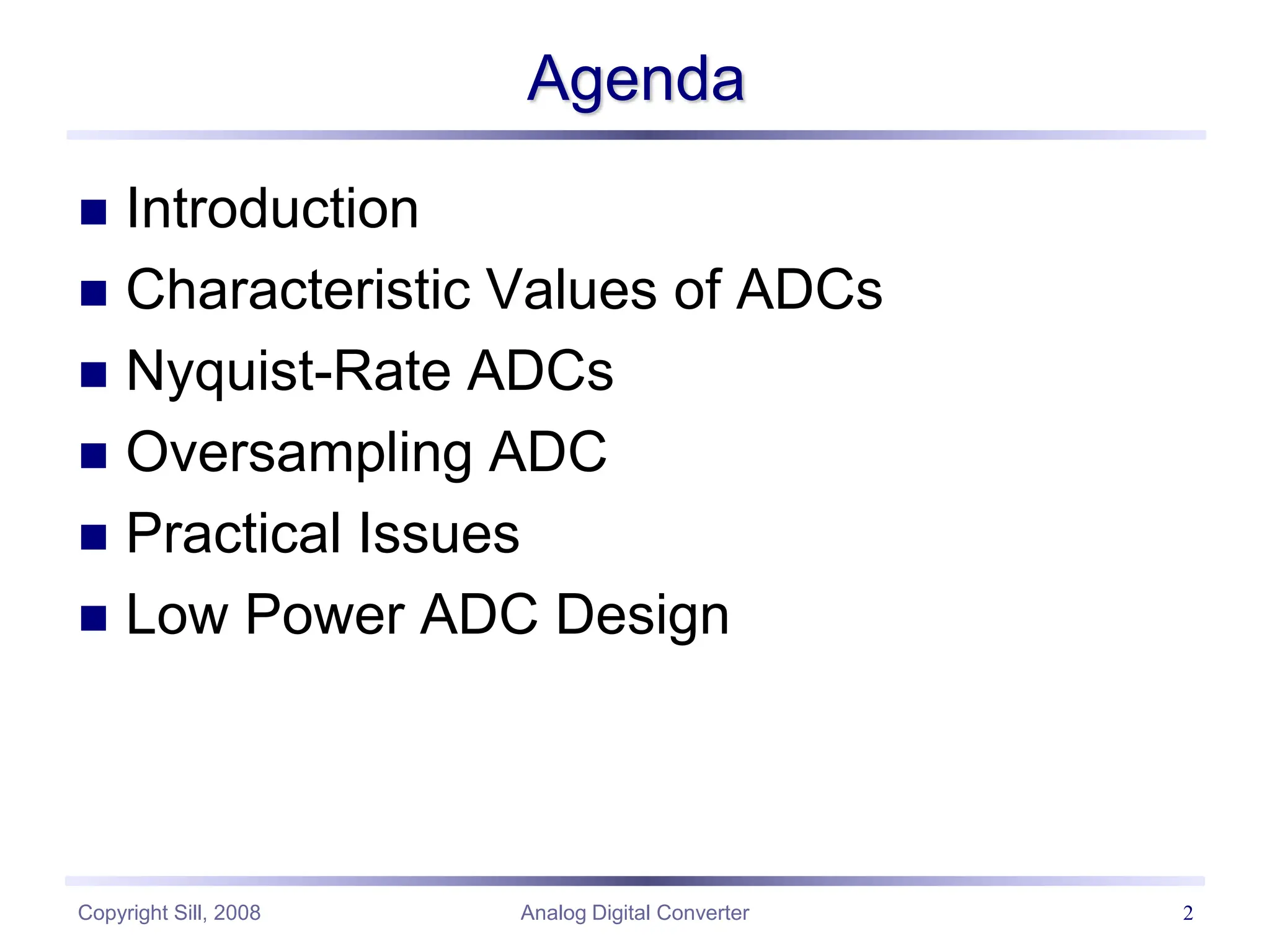
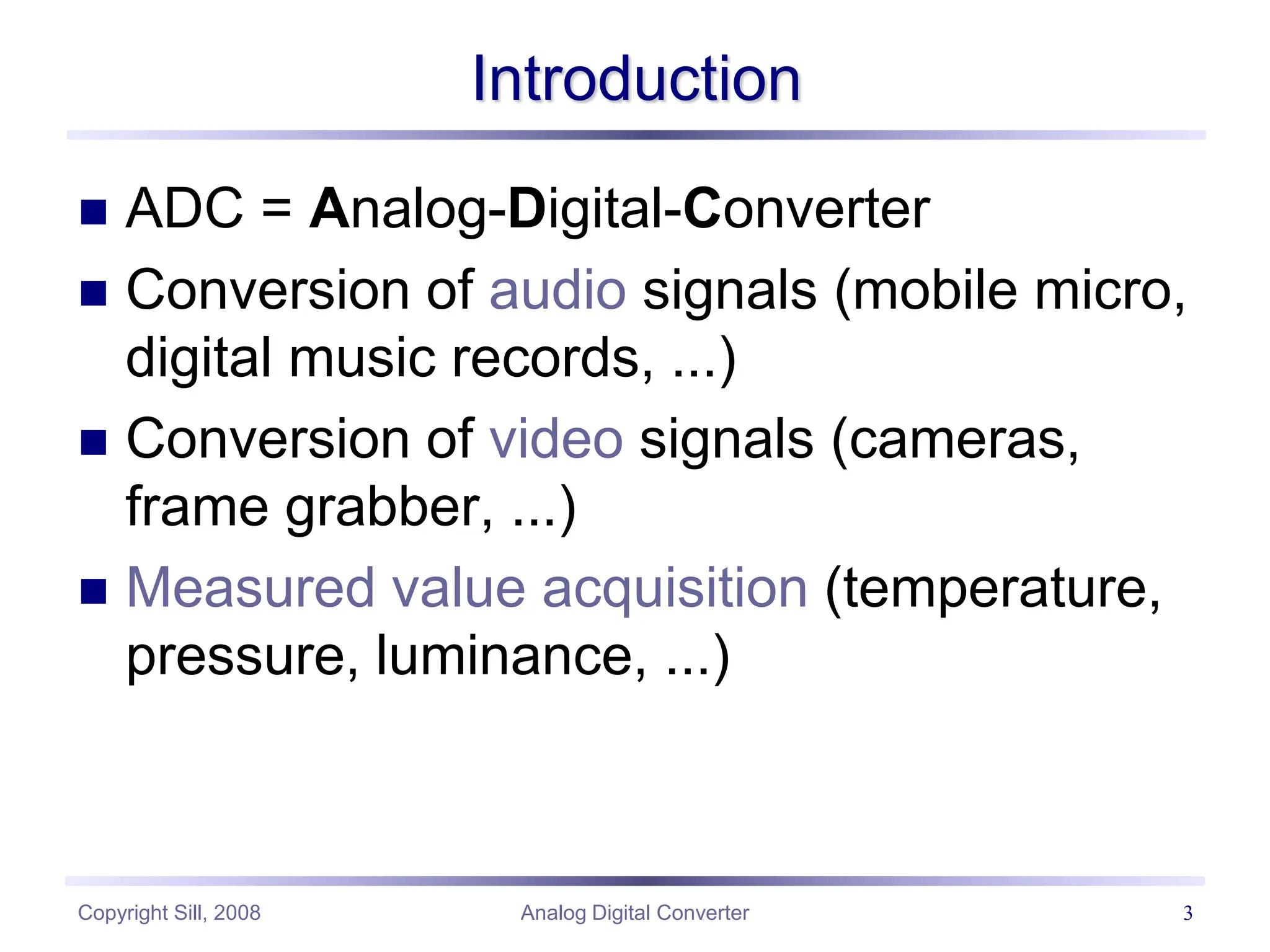
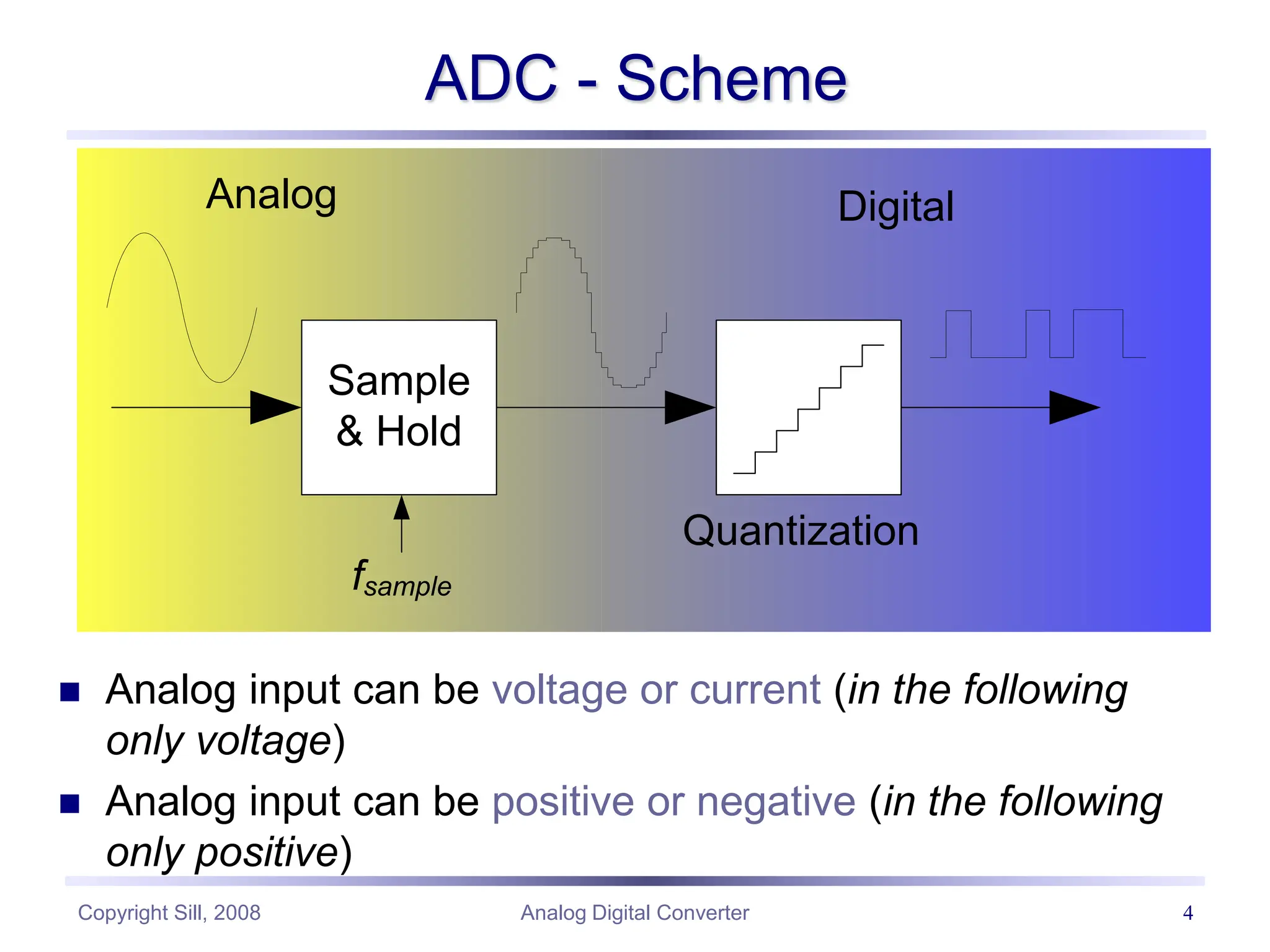
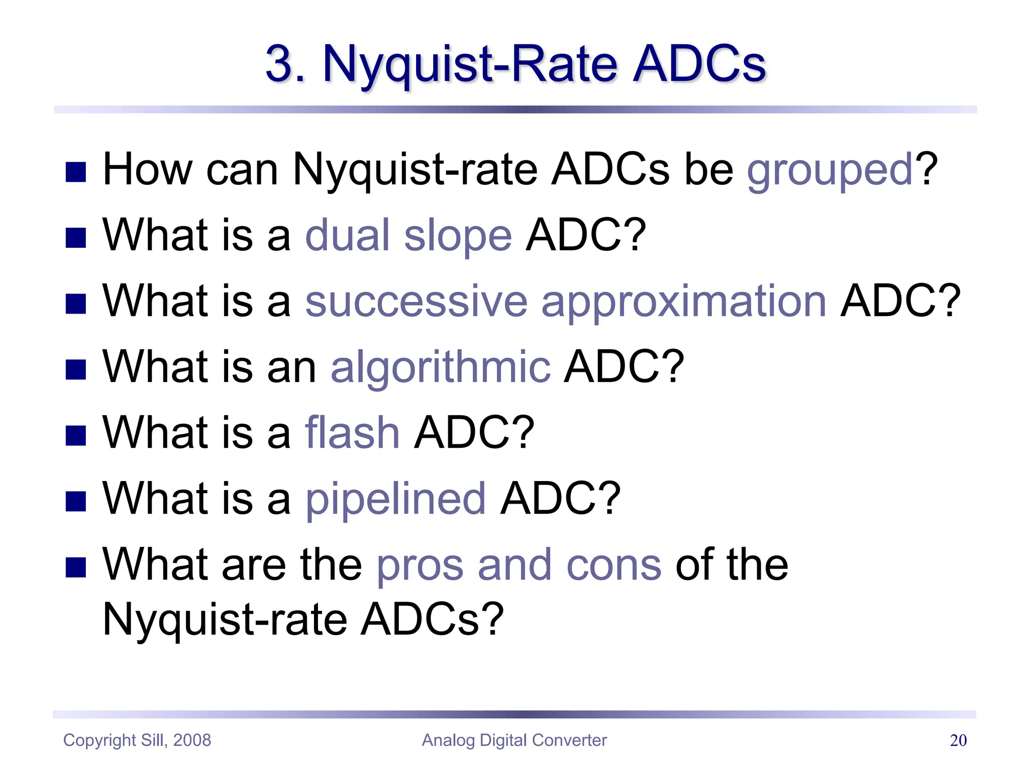
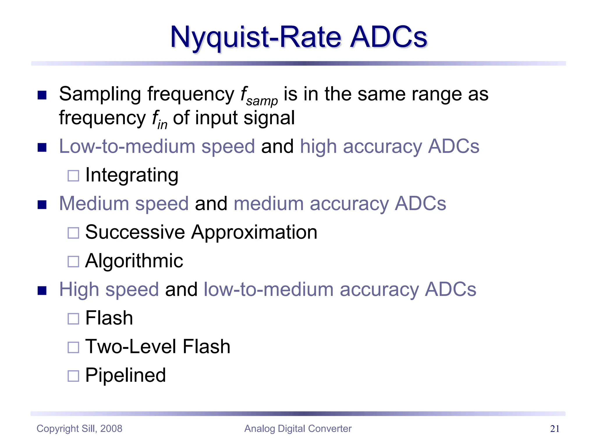
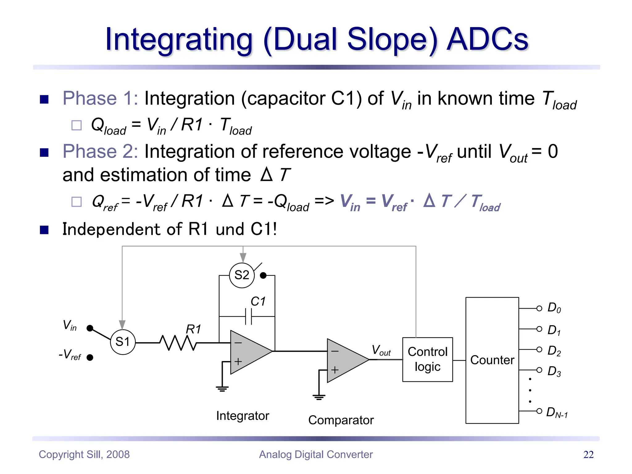
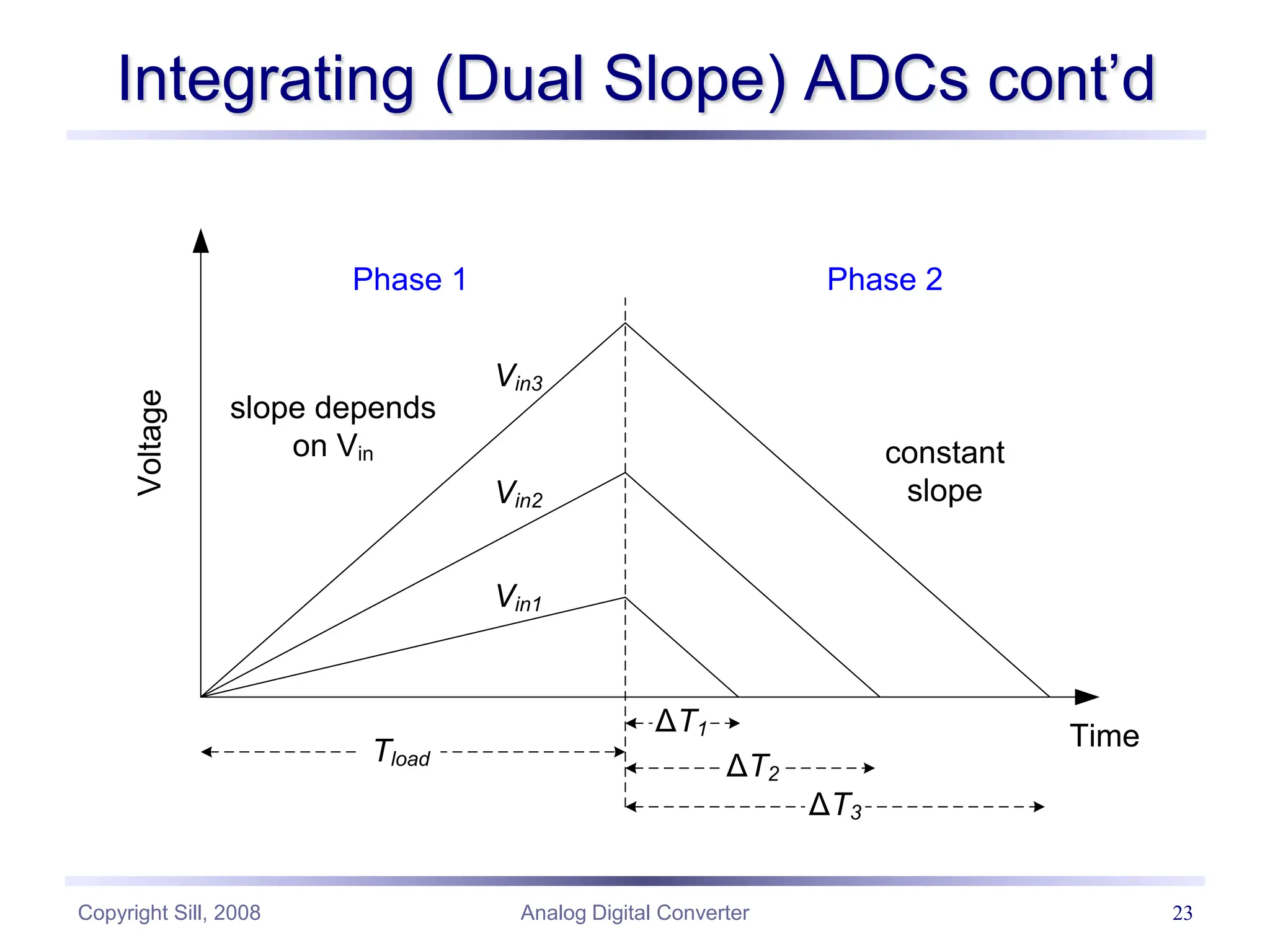
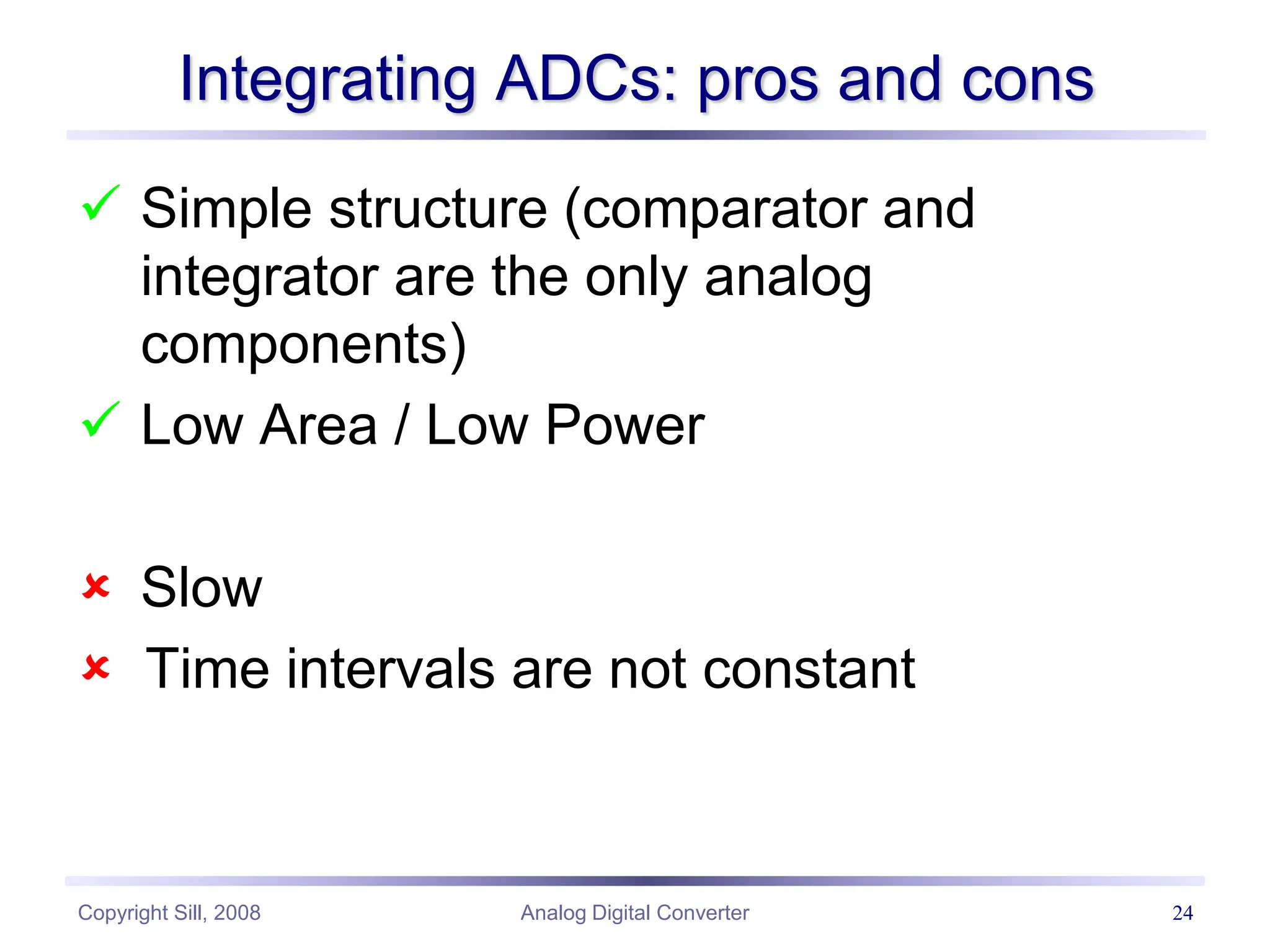
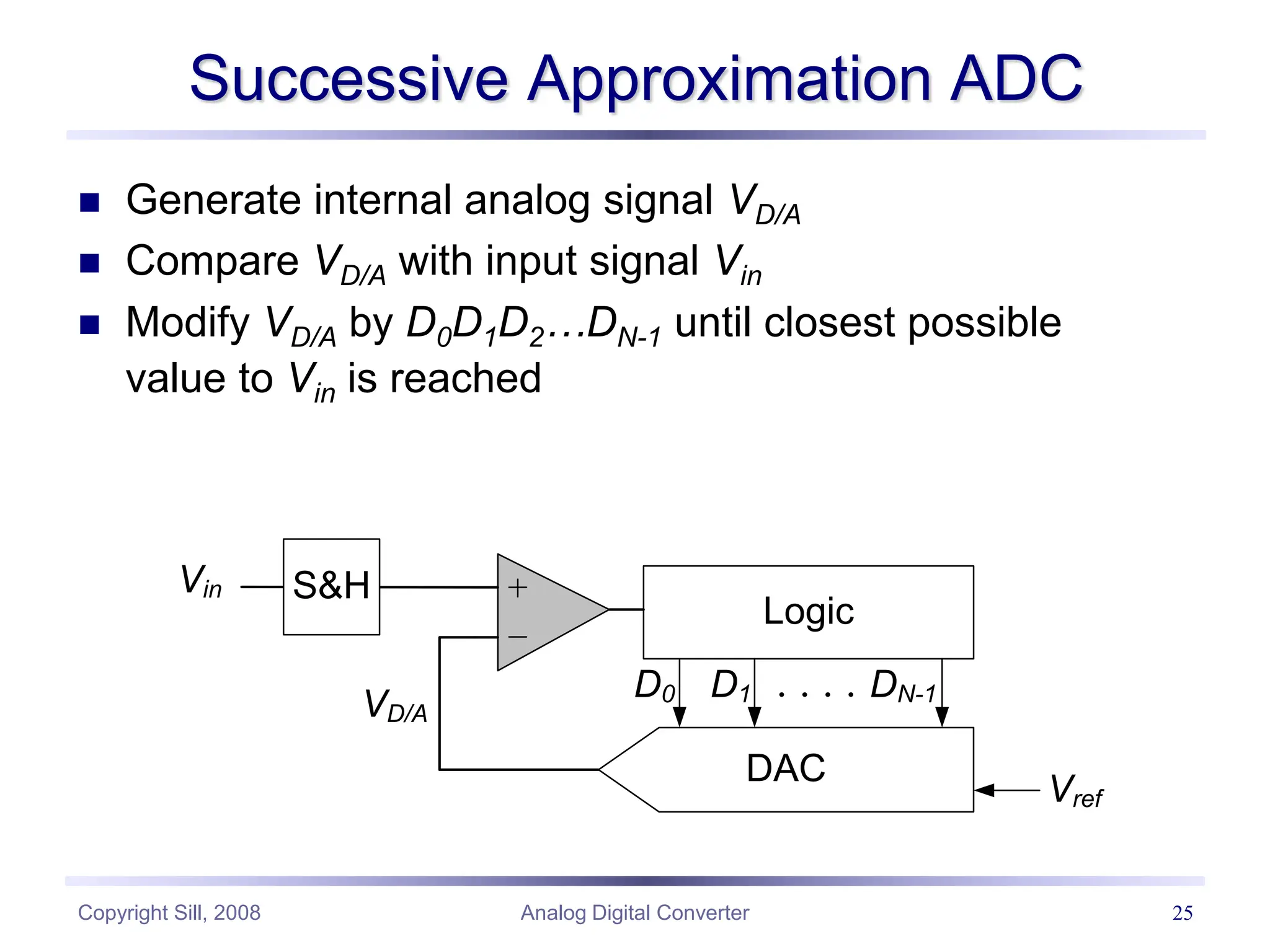
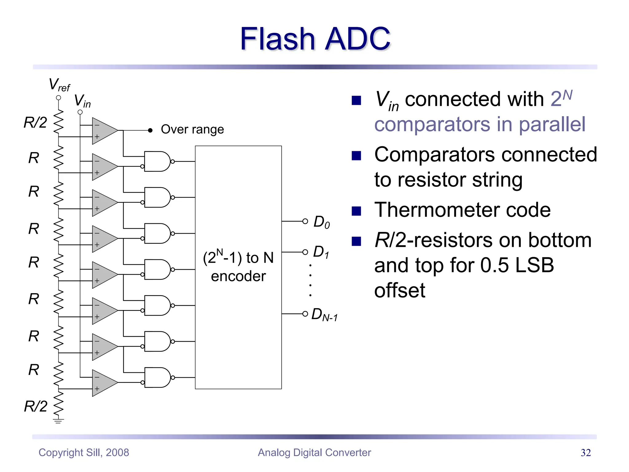
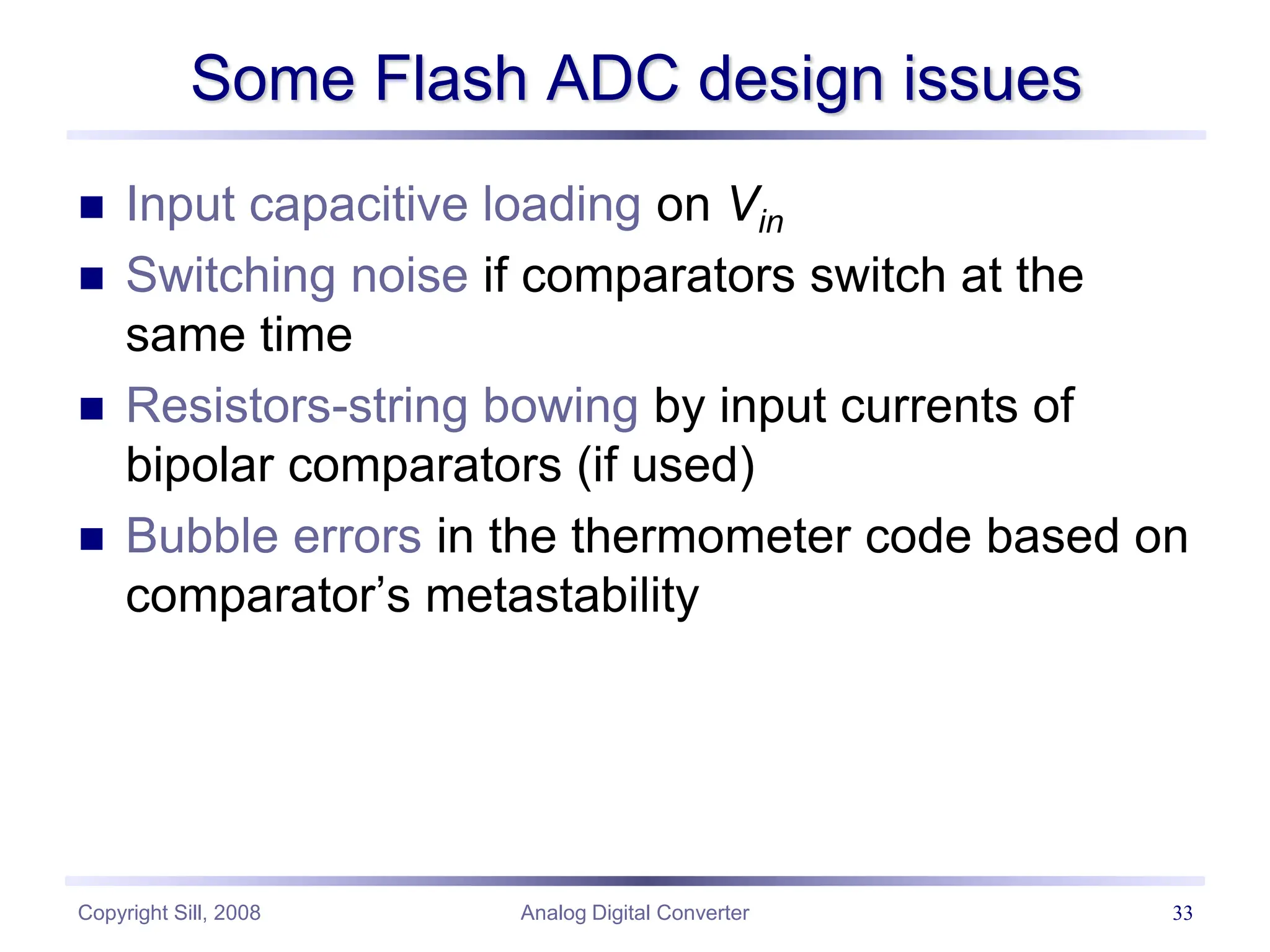
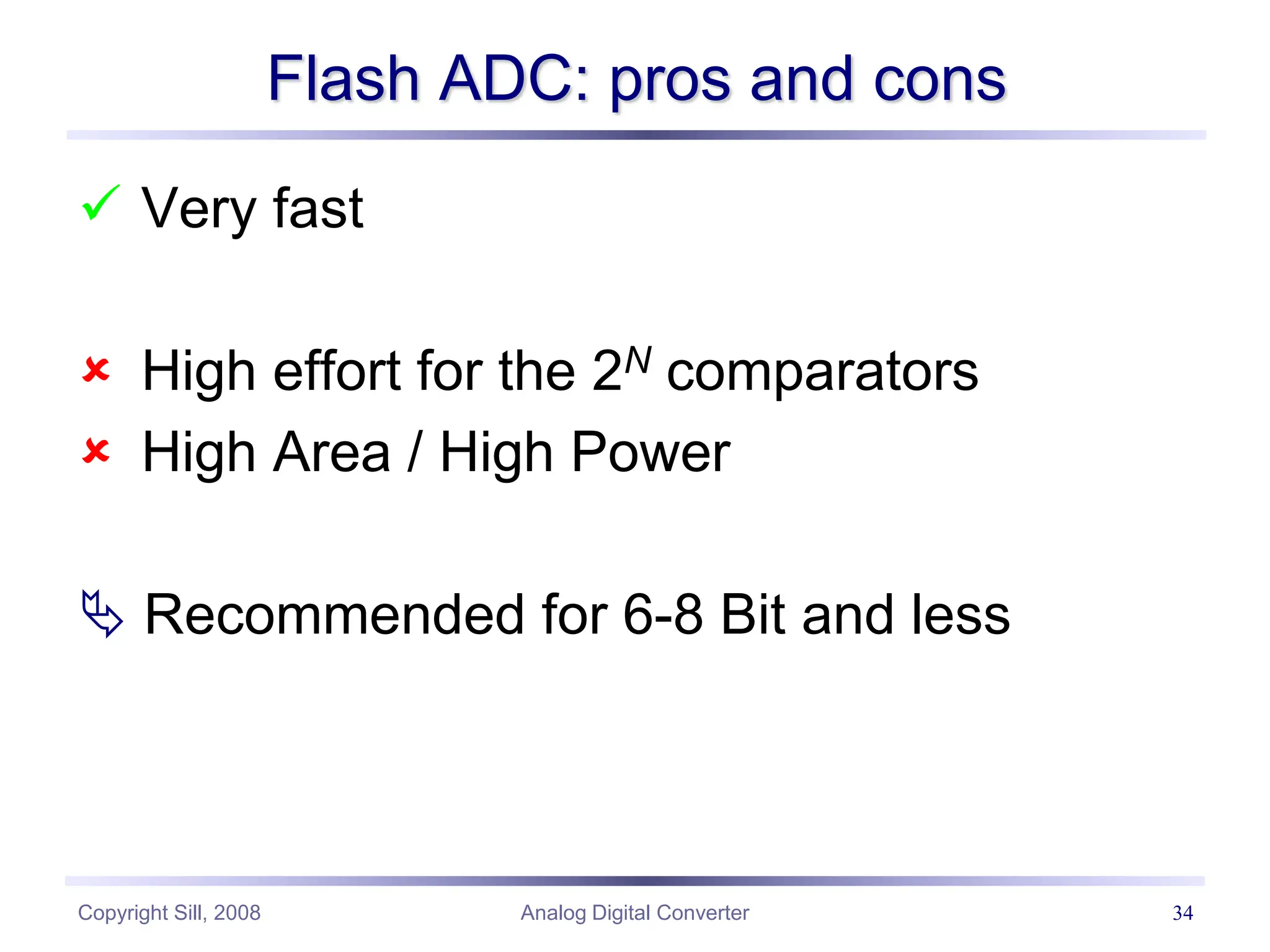
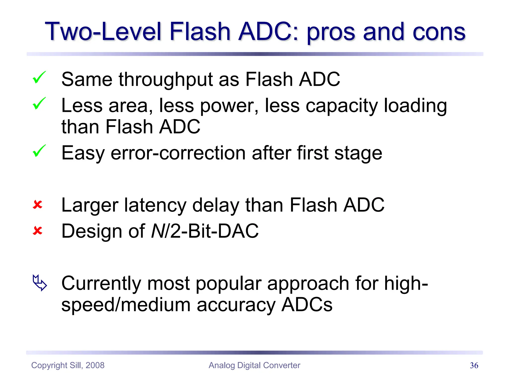
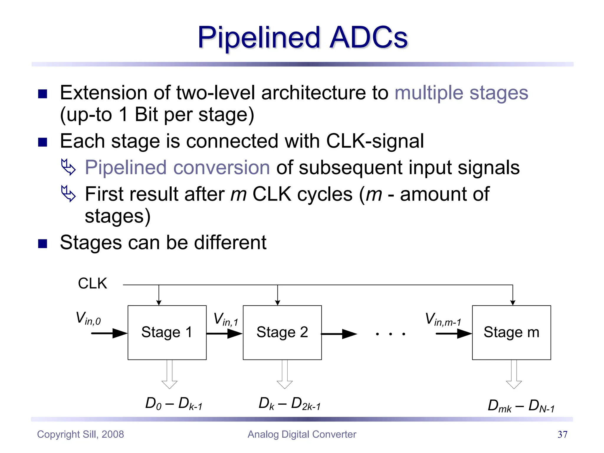
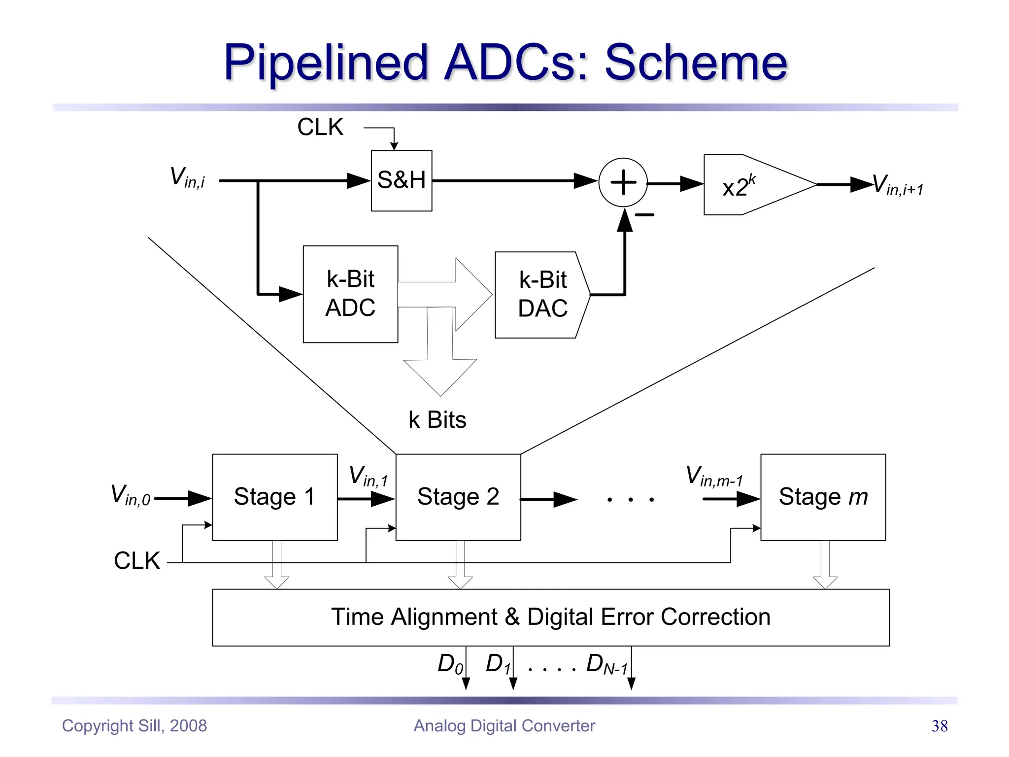
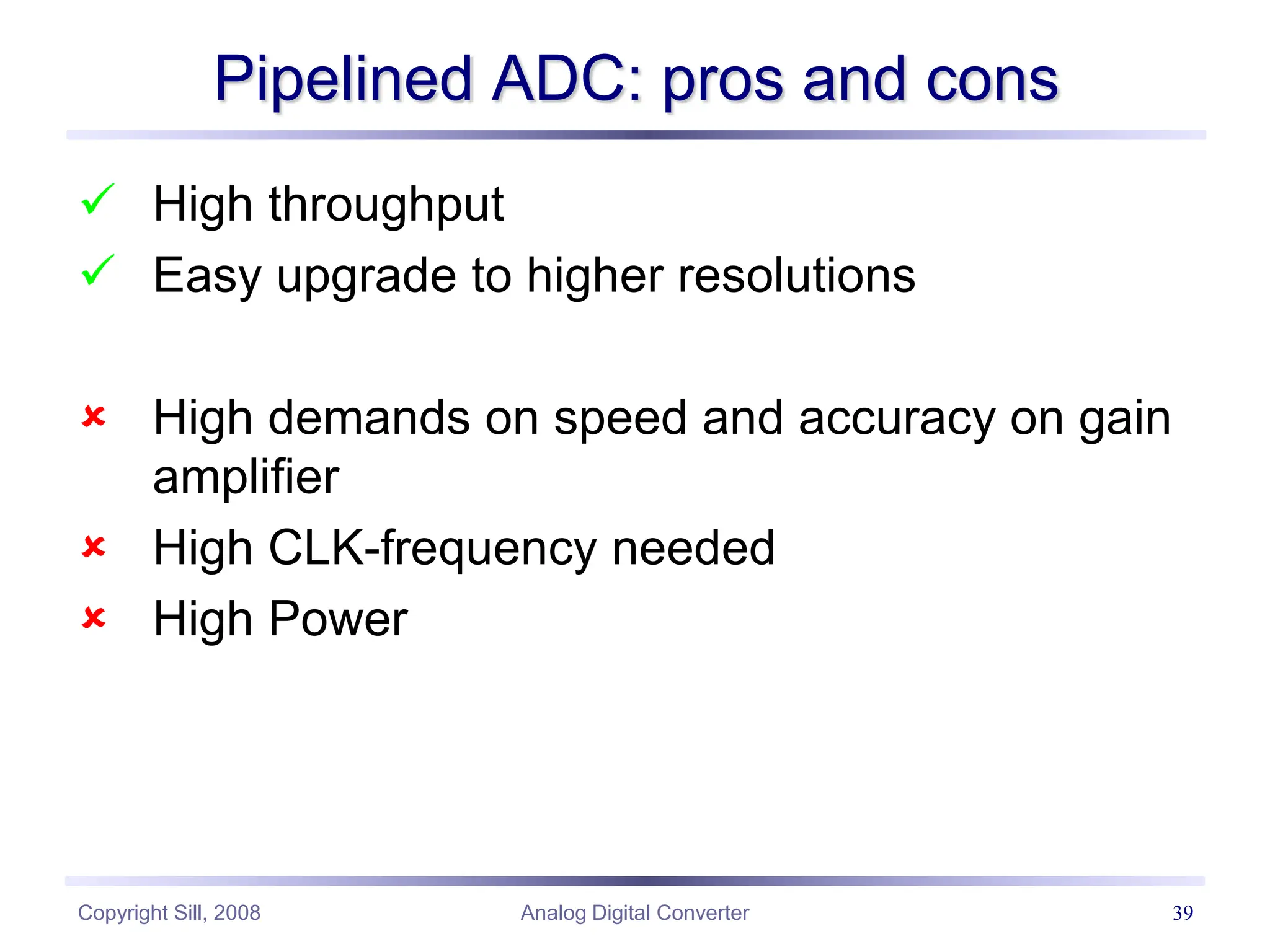
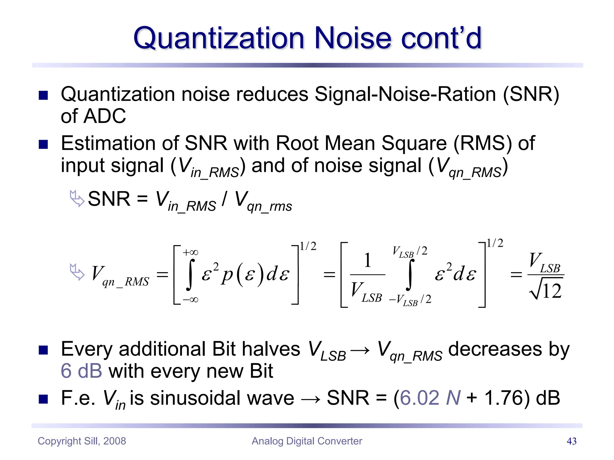
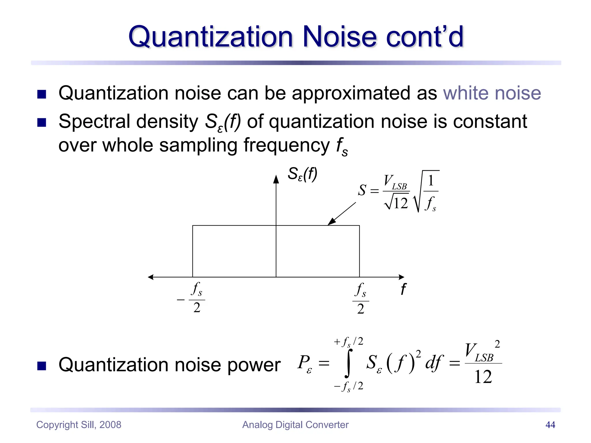
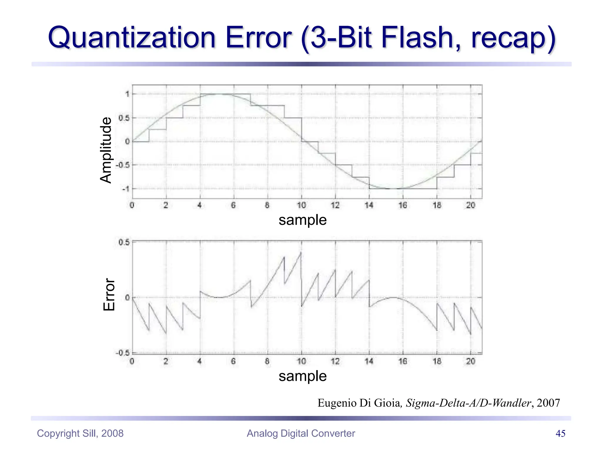
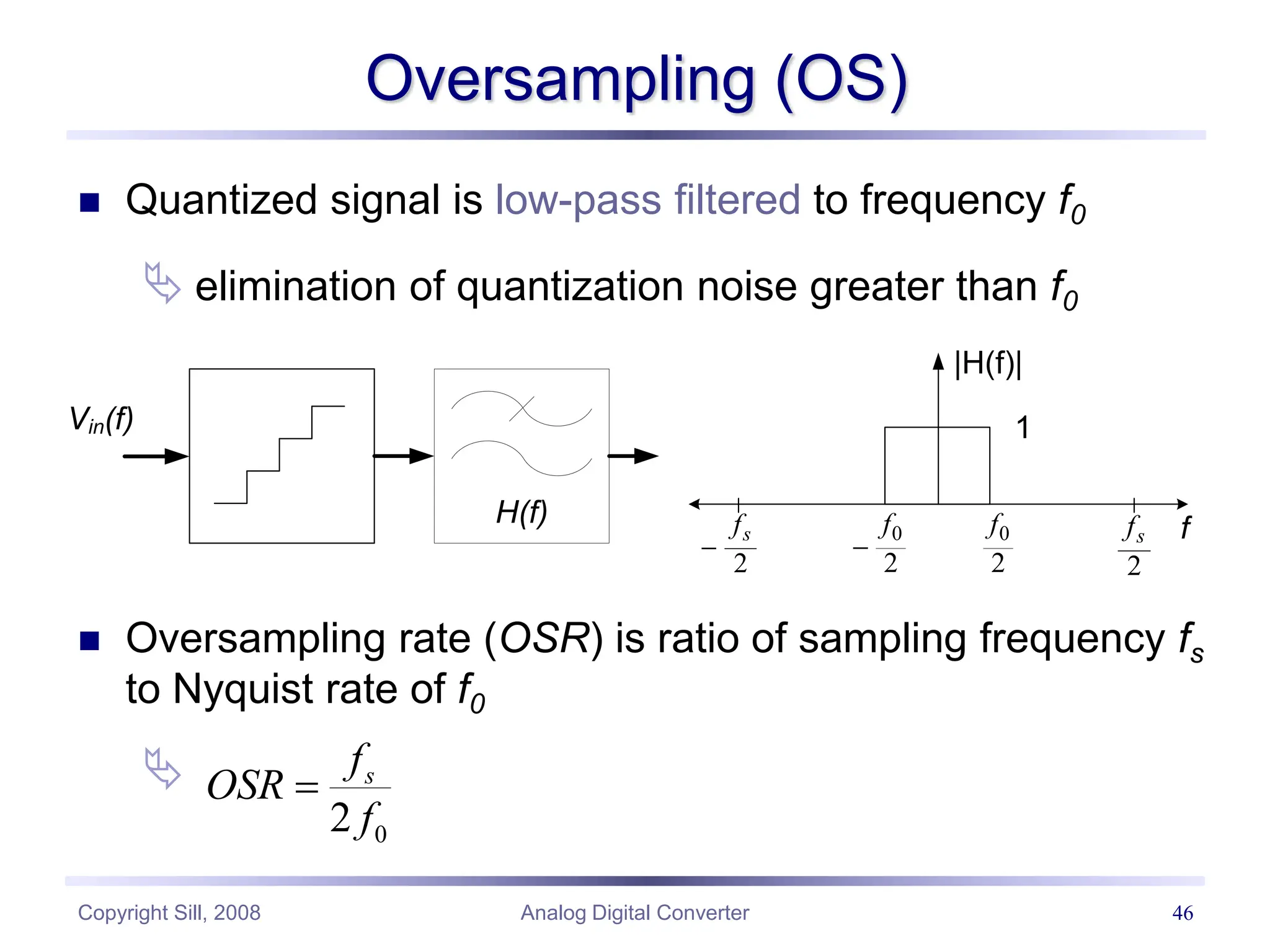
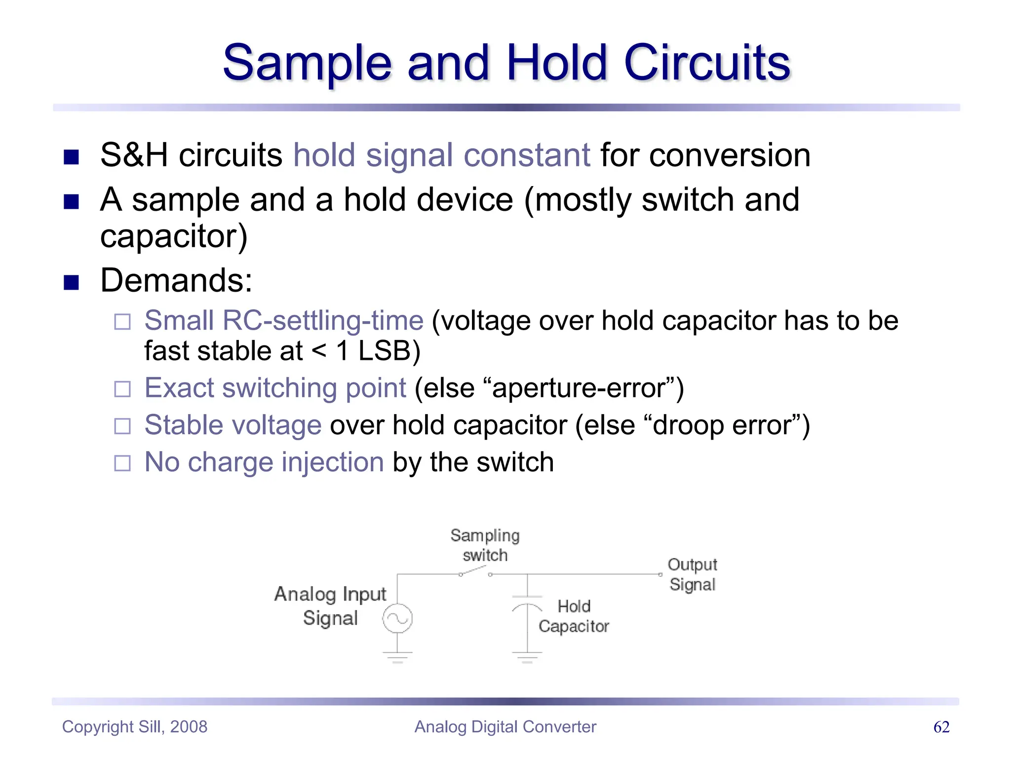
This document provides an introduction and overview of analog-to-digital converters (ADCs). It discusses key ADC characteristics and values such as resolution, reference voltage, least significant bit, full scale range, and errors. It also describes several common types of Nyquist-rate ADCs, including dual-slope integrating ADCs, successive approximation ADCs, algorithmic ADCs, flash ADCs, and pipelined ADCs. For each ADC type, it highlights pros and cons in terms of speed, accuracy, power, and area requirements.

![Copyright Sill, 2008 Analog Digital Converter 48
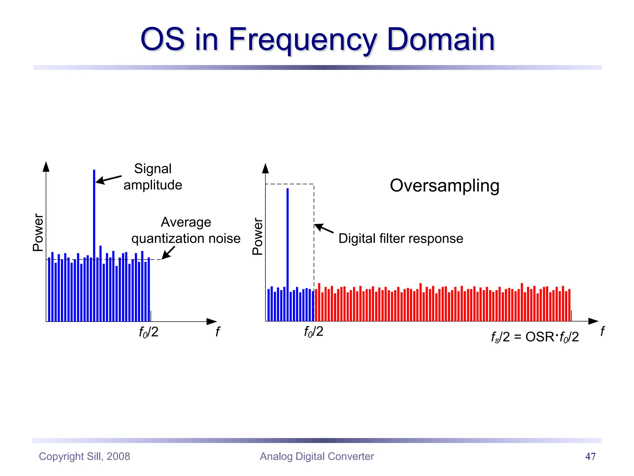
Oversampling cont’d
Quantization noise power Pε results to:
Doubling of fs increases SNR by 3 dB
Equivalently to a increase of resolution by 0.5 Bits
F.e. Vin is sinusoidal wave
SNR = (6.02 N + 1.76 + 10log [OSR]) dB
0
0
/2 /2 2
2
2 2
/2 /2
1
( ) ( )
12
s
s
f f
LS
f
B
f
V
P S f H f df S df
OSR
](https://image.slidesharecdn.com/analog-digital-converter-240413085535-6c259fd9/75/Analog-Digital-Converter-for-nyquiest-model-ppt-48-2048.jpg)
![Copyright Sill, 2008 Analog Digital Converter 49
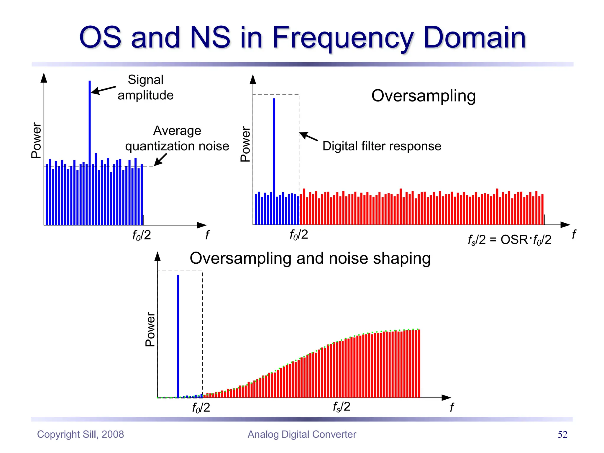
OS signal reconstruction
Signal results from relation of “0”s and “1”s
n
Nyquist -ADC
Oversampling - ADC
1V
0.66 V
0.33 V
Nyquist - ADC
Oversampling 00000011111111110000000
0.33 0.33
x[n]
2 2
_
0.33 0.33
2
RMS Nyquist
V
2 2 2 2
_
5 1 7 0 5 1 7 0
24
RMS Oversampling
V
](https://image.slidesharecdn.com/analog-digital-converter-240413085535-6c259fd9/75/Analog-Digital-Converter-for-nyquiest-model-ppt-49-2048.jpg)
![Copyright Sill, 2008 Analog Digital Converter 51
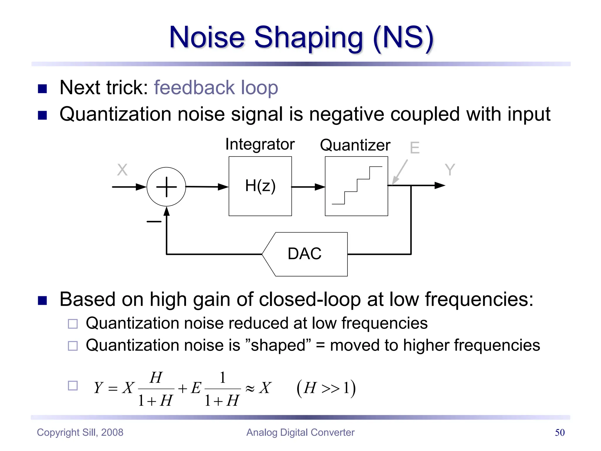
Noise Shaping cont’d
Oversampling and noise shaping:
Doubling of fs increases SNR by 9 dB
Equivalently to a increase of resolution by 1.5 Bits
F.e. Vin is sinusoidal wave
SNR = (6.02 N + 1.76 – 5.17 + 30log [OSR]) dB
up to fin = 100 kHz (and more)
1-Bit Quantizer (Comperator)
1-Bit DAC](https://image.slidesharecdn.com/analog-digital-converter-240413085535-6c259fd9/75/Analog-Digital-Converter-for-nyquiest-model-ppt-51-2048.jpg)
![Copyright Sill, 2008 Analog Digital Converter 74
Basic ADC Literature
[All02] P. E. Allen, D. R. Holberg, “CMOS Analog Circuit Design”,
Oxford University Press, 2002
[Azi96] P.M. Aziz, H. V. Sorensen, J. Van der Spiegel, "An
Overview of Sigma-Delta Converters" IEEE Signal
Processing Magazine, 1996
[Eu07] E. D. Gioia, “Sigma-Delta-A/D-Wandler”, 2007
[Fi05] P. Fischer, “VLSI-Design 0405 - ADC und DAC”, Uni
Mannheim, 2005
[Man02] Mancini, “Opamps for everyone”, Texas Instr., 2002
[Joh97] D. A. Johns, K. Martin, “Analog Integrated Circuit design”,
John Wiley & Sons, 1997
[Tan00] S. Tanner, “Low-power architectures for single-chip digital
image sensors”, dissertation, University of Neuchatel,
Switzerland, 2000.](https://image.slidesharecdn.com/analog-digital-converter-240413085535-6c259fd9/75/Analog-Digital-Converter-for-nyquiest-model-ppt-74-2048.jpg)

![Copyright Sill, 2008 Analog Digital Converter 76
Signal Reconstruction
Continuous time (input signal):
Discrete (reconstructed by ADC):
/ 2 2
_
/ 2
( )
T
RMS ct
T
v t
V dt
T
v(t)
time
2
0
_
[ ]
n
i
RMS discrete
x n
V
n
x[n]
n
RMS: root mean square](https://image.slidesharecdn.com/analog-digital-converter-240413085535-6c259fd9/75/Analog-Digital-Converter-for-nyquiest-model-ppt-76-2048.jpg)
![Copyright Sill, 2008 Analog Digital Converter 77
Voltage supply reduction [Tan00]
For analog design, it is
shown that a voltage
supply reduction does not
always lead to a power
consumption reduction for
several reasons:
Threshold of MOS
transistors.
Loss of maximal amplitudes
(SNR degradation).
Limits of conduction in
analog switches.
Low speed of MOS
transistors.
Limited stack of transistors.
0
0.5
1
1.5
2
2.5
3
0 1 2 3 4 5 6
Supply Voltage [V]
Power
Dissipation
[mW/MS/s]
Power consumption of 10-bit S-C
1.5 bit/stage pipelined ADCs in
function of the voltage supply.
[Tan00] S. Tanner, Low-power architectures for
single-chip digital image sensors, dissertation,
University of Neuchatel, Switzerland, 2000.](https://image.slidesharecdn.com/analog-digital-converter-240413085535-6c259fd9/75/Analog-Digital-Converter-for-nyquiest-model-ppt-77-2048.jpg)