Download as PPSX, PPTX

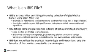
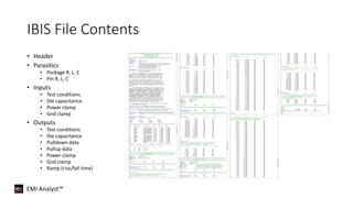
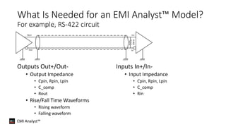
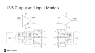
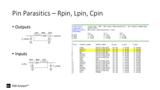
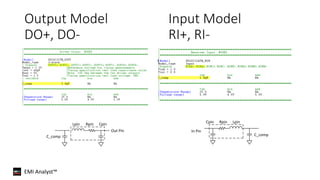
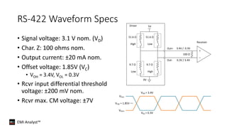
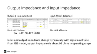
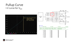
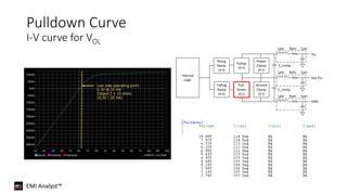
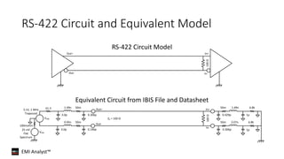
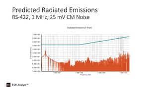
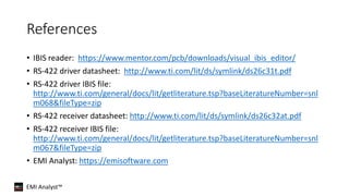

The document provides detailed information about the EMI Analyst™ software and the IBIS (Input/Output Buffer Information Specification) file format, which describes the analog behavior of digital device buffers. It outlines the required components and parameters for modeling RS-422 circuits, including output and input impedance, waveform specifications, and various electrical characteristics. Additionally, it includes references to relevant datasheets and online resources for further information.