Download as PDF, PPTX


![Estimated IIP3
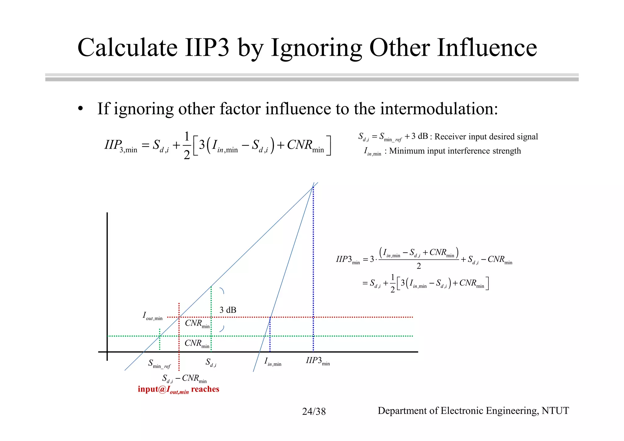
• If ignoring other factor influence to the intermodulation:
( )3,min , ,min , min
1
3
2
d i in d iIIP S I S CNR = + − +
[ ]3,min
1
99 3 49 8 21.5 dBm
2GSM
IIP = − + × + = −
[ ]3,min
1
107 3 62 9 9.5 dBm
2TDMA
IIP = − + × + = −
[ ]3,min
1
113 3 65 3 14 dBm for close-spaced
2AMPS
IIP = − + × + = −
[ ]3,min
1
113 3 70 3 6.5 dBm for wide-spaced
2AMPS
IIP = − + × + = −
Spec. GSM/GPRS TDMA AMPS
Desired signal −99 dBm −107 dBm −113 dBm
Spurious Response
Attenuation
49 dBc 62 dBc
close wide
65 dBc 70 dBc
CNRmin 8 dB 9 dB 3 dB 3 dB
Required IIP3 −21.5 dBm −9.5 dBm −14 dBm −6.5 dBm
Department of Electronic Engineering, NTUT25/38](https://image.slidesharecdn.com/ch7-150613070936-lva1-app6892/75/Multiband-Transceivers-Chapter-7-Multi-mode-Multi-band-GSM-GPRS-TDMA-AMPS-System-Analysis-25-2048.jpg)


This document presents an analysis of a multiband/multi-mode RF transceiver system for GSM, GPRS, TDMA, and AMPS mobile systems, detailing its architecture, specifications, and performance evaluation. Key topics include calculations for noise figure, linearity requirements, selectivity, blocking performance, and a comprehensive frequency plan. The analysis aims to ensure reliable and efficient operation across various operating modes while considering impairment factors and required performance metrics.

![Multiband Transceivers - [Chapter 2] Noises and Linearities](https://cdn.slidesharecdn.com/ss_thumbnails/ch2-150613070933-lva1-app6892-thumbnail.jpg?width=640&height=640&fit=bounds)
![RF Module Design - [Chapter 4] Transceiver Architecture](https://cdn.slidesharecdn.com/ss_thumbnails/rfch4-150613070346-lva1-app6891-thumbnail.jpg?width=640&height=640&fit=bounds)
![Multiband Transceivers - [Chapter 1]](https://cdn.slidesharecdn.com/ss_thumbnails/ch1-150613070932-lva1-app6891-thumbnail.jpg?width=640&height=640&fit=bounds)

![RF Module Design - [Chapter 1] From Basics to RF Transceivers](https://cdn.slidesharecdn.com/ss_thumbnails/rfch1-150613070344-lva1-app6892-thumbnail.jpg?width=640&height=640&fit=bounds)


![Multiband Transceivers - [Chapter 5] Software-Defined Radios](https://cdn.slidesharecdn.com/ss_thumbnails/ch5-150613070934-lva1-app6892-thumbnail.jpg?width=640&height=640&fit=bounds)
![Multiband Transceivers - [Chapter 4] Design Parameters of Wireless Radios](https://cdn.slidesharecdn.com/ss_thumbnails/ch4-150613070934-lva1-app6892-thumbnail.jpg?width=640&height=640&fit=bounds)
![Multiband Transceivers - [Chapter 6] Multi-mode and Multi-band Transceivers](https://cdn.slidesharecdn.com/ss_thumbnails/ch6-150613070935-lva1-app6891-thumbnail.jpg?width=640&height=640&fit=bounds)


![RF Module Design - [Chapter 7] Voltage-Controlled Oscillator](https://cdn.slidesharecdn.com/ss_thumbnails/rfch7-150613070347-lva1-app6892-thumbnail.jpg?width=640&height=640&fit=bounds)


![RF Module Design - [Chapter 6] Power Amplifier](https://cdn.slidesharecdn.com/ss_thumbnails/rfch6-150613070347-lva1-app6891-thumbnail.jpg?width=640&height=640&fit=bounds)

![RF Circuit Design - [Ch4-2] LNA, PA, and Broadband Amplifier](https://cdn.slidesharecdn.com/ss_thumbnails/ch4-2-150613064410-lva1-app6891-thumbnail.jpg?width=640&height=640&fit=bounds)


![Multiband Transceivers - [Chapter 3] Basic Concept of Comm. Systems](https://cdn.slidesharecdn.com/ss_thumbnails/ch3-150613070933-lva1-app6892-thumbnail.jpg?width=640&height=640&fit=bounds)
![RF Module Design - [Chapter 5] Low Noise Amplifier](https://cdn.slidesharecdn.com/ss_thumbnails/rfch5-150613070346-lva1-app6891-thumbnail.jpg?width=640&height=640&fit=bounds)
![Multiband Transceivers - [Chapter 7] Spec. Table](https://cdn.slidesharecdn.com/ss_thumbnails/ch7table-150613070936-lva1-app6892-thumbnail.jpg?width=640&height=640&fit=bounds)
![RF Module Design - [Chapter 2] Noises](https://cdn.slidesharecdn.com/ss_thumbnails/rfch2-150613070344-lva1-app6892-thumbnail.jpg?width=640&height=640&fit=bounds)

![RF Module Design - [Chapter 3] Linearity](https://cdn.slidesharecdn.com/ss_thumbnails/rfch3-150613070345-lva1-app6891-thumbnail.jpg?width=640&height=640&fit=bounds)

![RF Module Design - [Chapter 8] Phase-Locked Loops](https://cdn.slidesharecdn.com/ss_thumbnails/rfch8-150613070348-lva1-app6892-thumbnail.jpg?width=640&height=640&fit=bounds)

![Agilent ADS 模擬手冊 [實習1] 基本操作與射頻放大器設計](https://cdn.slidesharecdn.com/ss_thumbnails/1adsbasics-150613072812-lva1-app6891-thumbnail.jpg?width=640&height=640&fit=bounds)
![射頻電子實驗手冊 [實驗6] 阻抗匹配模擬](https://cdn.slidesharecdn.com/ss_thumbnails/simlab6-150613072411-lva1-app6892-thumbnail.jpg?width=640&height=640&fit=bounds)


![[嵌入式系統] MCS-51 實驗 - 使用 IAR (2)](https://cdn.slidesharecdn.com/ss_thumbnails/mcs51iarpart2-150613071717-lva1-app6891-thumbnail.jpg?width=640&height=640&fit=bounds)
![[嵌入式系統] 嵌入式系統進階](https://cdn.slidesharecdn.com/ss_thumbnails/advembedded-150613071653-lva1-app6892-thumbnail.jpg?width=640&height=640&fit=bounds)
![[ZigBee 嵌入式系統] ZigBee 應用實作 - 使用 TI Z-Stack Firmware](https://cdn.slidesharecdn.com/ss_thumbnails/zigbeeappimplementation-150613072040-lva1-app6891-thumbnail.jpg?width=640&height=640&fit=bounds)
![[嵌入式系統] MCS-51 實驗 - 使用 IAR (1)](https://cdn.slidesharecdn.com/ss_thumbnails/mcs51iarpart1-150613071712-lva1-app6892-thumbnail.jpg?width=640&height=640&fit=bounds)
![[嵌入式系統] MCS-51 實驗 - 使用 IAR (3)](https://cdn.slidesharecdn.com/ss_thumbnails/mcs51iarpart3-150613071723-lva1-app6892-thumbnail.jpg?width=640&height=640&fit=bounds)


![射頻電子實驗手冊 [實驗1 ~ 5] ADS入門, 傳輸線模擬, 直流模擬, 暫態模擬, 交流模擬](https://cdn.slidesharecdn.com/ss_thumbnails/simlab15-150613072411-lva1-app6892-thumbnail.jpg?width=640&height=640&fit=bounds)
![射頻電子實驗手冊 - [實驗7] 射頻放大器模擬](https://cdn.slidesharecdn.com/ss_thumbnails/simlab7-150613072420-lva1-app6892-thumbnail.jpg?width=640&height=640&fit=bounds)
![射頻電子實驗手冊 - [實驗8] 低雜訊放大器模擬](https://cdn.slidesharecdn.com/ss_thumbnails/simlab8-150613072425-lva1-app6891-thumbnail.jpg?width=640&height=640&fit=bounds)
![Agilent ADS 模擬手冊 [實習2] 放大器設計](https://cdn.slidesharecdn.com/ss_thumbnails/2adsamp-150613072818-lva1-app6892-thumbnail.jpg?width=640&height=640&fit=bounds)
![Agilent ADS 模擬手冊 [實習3] 壓控振盪器模擬](https://cdn.slidesharecdn.com/ss_thumbnails/3adsosc-150613072819-lva1-app6892-thumbnail.jpg?width=640&height=640&fit=bounds)
![[ZigBee 嵌入式系統] ZigBee Architecture 與 TI Z-Stack Firmware](https://cdn.slidesharecdn.com/ss_thumbnails/zigbeearchitecture-150613072045-lva1-app6892-thumbnail.jpg?width=640&height=640&fit=bounds)


