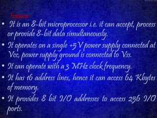
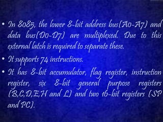
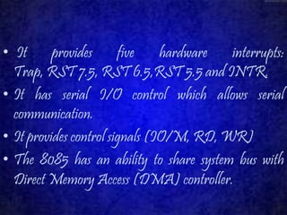
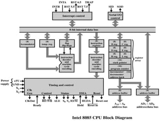
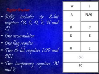
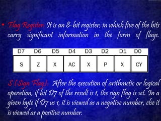
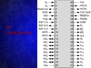
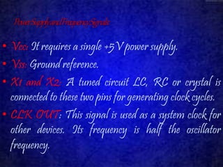
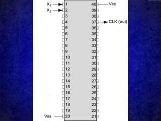
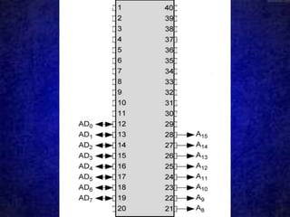
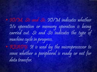
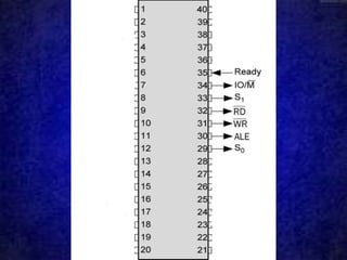
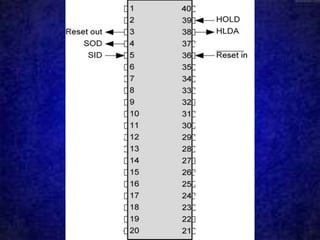
Features:- 
• It is an 8-bit microprocessor i.e. it can accept, process 
or provide 8-bit data simultaneously. 
• It operates on a single +5V power supply connected at 
Vcc, power supply ground is connected to Vss. 
• It can operate with a 3 MHz clock frequency. 
• It has 16 address lines, hence it can access 64 Kbytes 
of memory. 
• It provides 8 bit I/O addresses to access 256 I/O 
ports.
• In 8085, the lower 8-bit address bus(A0-A7) and 
data bus(D0-D7) are multiplexed. Due to this 
external latch is required to separate these. 
• It supports 74 instructions. 
• It has 8-bit accumulator, flag register, instruction 
register, six 8-bit general purpose registers 
(B,C,D,E,H and L) and two 16-bit registers (SP 
and PC).
• It provides five hardware interrupts: 
Trap, RST 7.5, RST 6.5,RST 5.5 and INTR. 
• It has serial I/O control which allows serial 
communication. 
• It provides control signals (IO/M, RD, WR) 
• The 8085 has an ability to share system bus with 
Direct Memory Access (DMA) controller.
Architecture of 8085 
It consists of various functional blocks as listed below: 
• Registers 
• ALU 
• Instruction decoder and machine cycle encoder 
• Address buffer and Data Buffer 
• Interrupt control 
• Serial I/O control 
• Timing and control circuitry
Register Structure 
• 8085 includes six 8-bit 
registers (B, C, D, E, H and 
L) 
• One accumulator 
• One flag register 
• Two 16-bit registers (SP and 
PC) 
• Two temporary registers W 
and Z
• General Purpose Register: B, C, D, E, H and L are 
8-bit general purpose register can be as a separate 8- 
bit registers or as 16-bit register pairs, BC, DE and 
HL. 
• Temporary Register: The ALU has two inputs, one 
input is supplied by the accumulator and other from 
temporary data register. These are internally used for 
execution of most of the arithmetic and logical 
instructions.
• Special Purpose Register:- 
Accumulator: It is an 8-bit register. It is 
extensively used in arithmetic, logic, load and store 
operations, as well as in input/output operations. 
Most of the times the result of arithmetic and 
logical operations is stored in the accumulator.
• Flag Register: It is an 8-bit register, in which five of the bits 
carry significant information in the form of flags. 
S (Sign Flag): After the execution of arithmetic or logical 
operation, if bit D7 of the result is 1, the sign flag is set. In a 
given byte if D7 us 1, it is viewed as a negative number, else it 
is viewed as a positive number.
Z (Zero Flag): The zero flag is set if the result of 
operation in ALU is zero and flag resets if result is 
non zero. 
AC (Auxiliary Carry Flag): This flag is set if 
there is an overflow out of bit 3, i.e. carry from 
lower nibble to higher nibble(D3 to D4). This flag 
is used for BCD operations.
P(Parity Flag): Parity is defined by the number 
of ones present in the accumulator. After an 
operation if the result has an even number of ones, 
the flag is set, if the number is odd, flag is reset. 
CY(Carry Flag): This flag is set if there is an 
overflow out of bit 7. The carry flag also serves as a 
borrow flag for subtraction.
• Instruction Register: The CPU stores the opcode in a 
register called the instruction register. 
• Program Counter: It stores the address of the next 
instruction to be fetched. 
• Stack Pointer: It is the reserved area in the RAM 
where temporary information may be stored. It is 
used to store the address of the most recent stack entry.
Arithmetic Logic Unit 
The 8085’s ALU performs arithmetic and logical 
functions on eight variables. The arithmetic unit 
performs bitwise fundamental arithmetic operations 
such as addition and subtraction. The logic unit 
performs logical operations such as complement, 
AND, OR, EX-OR, rotate and clear. The ALU 
also looks after the branching decisions.
PIN 
CONFIGURATION:-
The signals of 8085 can be classified into seven groups 
according to there functions:- 
• Power Supply and Frequency signals 
• Data bus and address bus 
• Control bus 
• Interrupt signals 
• Serial I/O signals 
• DMAsignals 
• Reset Signals
Power Supply and Frequency Signals: 
• Vcc: It requires a single +5V power supply. 
• Vss: Ground reference. 
• X1 and X2: A tuned circuit LC, RC or crystal is 
connected to these two pins for generating clock cycles. 
• CLK OUT: This signal is used as a system clock for 
other devices. Its frequency is half the oscillator 
frequency.
Data Bus and Address Bus:- 
• AD0 to AD7: The 8-bit data bus(D0–D7) is 
multiplexed with the lower half of the 16 bit 
address bus(A0-A7). 
• A8 to A15: The upper half of the 16-bit address 
bus appears on the address lines A8 to A15. 
These lines are most significant 8 bits of the 16- 
bit address lines.
Control and Status Signals:- 
• ALE(Address Latch enable): The latching of lower half 
of an address bus is done using an external latch and ALE 
signals. 
• RD and WR: These signals are basically used to control 
the direction of the data flow between processor and 
memory or I/O devices. A low on RD indicates that the 
data must be read from the selected memory location or 
I/O port via data bus. A low on WR indicates that the 
data must be written into the selected memory location or 
I/O port via data bus.
• IO/M, S0 and S1: IO/M indicates whether 
I/o operation or memory operation is being 
carried out. S1 and S0 indicates the type of 
machine cycle in progress. 
• READY: It is used by the microprocessor to 
sense whether a peripheral is ready or not for 
data transfer.
Interrupt Signals:- 
The 8085 has five hardware interrupt signals: RST 
5.5, RST 6.6, RST 7.5, TRAP and INTR. The 
microprocessor recognizes request on these lines at the 
end of the current instruction execution. 
The INTA(interrupt acknowledge) signal is used to 
indicate that the processor has acknowledged an 
INTR interrupt.
Serial I/O Signals 
• SID (Serial I/P Data): This input signal is 
used to accept serial data bit by bit from the 
external device. 
• SOD (Serial O/P Data): This is an output 
signal which enables the transmission of serial 
data bit to the external device.
DMA Signal 
• HOLD: This signal indicates that another 
master is requesting for the use of address bus, 
data bus and control bus. 
• HLDA: This activate high signal is used to 
acknowledge HOLD request.
Reset Signals 
• RESET IN: A low on the pin, Sets the PC to zero 
and Resets the interrupt enable and HLDA flip-flops. 
• RESET OUT: This active high signal indicates 
that processor is being reset. This signal is 
synchronized to the processor clock and it can be used 
to reset other devices connected to the system.
•

8085 microprocessor

  • 2.
    Features:- • Itis an 8-bit microprocessor i.e. it can accept, process or provide 8-bit data simultaneously. • It operates on a single +5V power supply connected at Vcc, power supply ground is connected to Vss. • It can operate with a 3 MHz clock frequency. • It has 16 address lines, hence it can access 64 Kbytes of memory. • It provides 8 bit I/O addresses to access 256 I/O ports.
  • 3.
    • In 8085,the lower 8-bit address bus(A0-A7) and data bus(D0-D7) are multiplexed. Due to this external latch is required to separate these. • It supports 74 instructions. • It has 8-bit accumulator, flag register, instruction register, six 8-bit general purpose registers (B,C,D,E,H and L) and two 16-bit registers (SP and PC).
  • 4.
    • It providesfive hardware interrupts: Trap, RST 7.5, RST 6.5,RST 5.5 and INTR. • It has serial I/O control which allows serial communication. • It provides control signals (IO/M, RD, WR) • The 8085 has an ability to share system bus with Direct Memory Access (DMA) controller.
  • 5.
    Architecture of 8085 It consists of various functional blocks as listed below: • Registers • ALU • Instruction decoder and machine cycle encoder • Address buffer and Data Buffer • Interrupt control • Serial I/O control • Timing and control circuitry
  • 7.
    Register Structure •8085 includes six 8-bit registers (B, C, D, E, H and L) • One accumulator • One flag register • Two 16-bit registers (SP and PC) • Two temporary registers W and Z
  • 8.
    • General PurposeRegister: B, C, D, E, H and L are 8-bit general purpose register can be as a separate 8- bit registers or as 16-bit register pairs, BC, DE and HL. • Temporary Register: The ALU has two inputs, one input is supplied by the accumulator and other from temporary data register. These are internally used for execution of most of the arithmetic and logical instructions.
  • 9.
    • Special PurposeRegister:- Accumulator: It is an 8-bit register. It is extensively used in arithmetic, logic, load and store operations, as well as in input/output operations. Most of the times the result of arithmetic and logical operations is stored in the accumulator.
  • 10.
    • Flag Register:It is an 8-bit register, in which five of the bits carry significant information in the form of flags. S (Sign Flag): After the execution of arithmetic or logical operation, if bit D7 of the result is 1, the sign flag is set. In a given byte if D7 us 1, it is viewed as a negative number, else it is viewed as a positive number.
  • 11.
    Z (Zero Flag):The zero flag is set if the result of operation in ALU is zero and flag resets if result is non zero. AC (Auxiliary Carry Flag): This flag is set if there is an overflow out of bit 3, i.e. carry from lower nibble to higher nibble(D3 to D4). This flag is used for BCD operations.
  • 12.
    P(Parity Flag): Parityis defined by the number of ones present in the accumulator. After an operation if the result has an even number of ones, the flag is set, if the number is odd, flag is reset. CY(Carry Flag): This flag is set if there is an overflow out of bit 7. The carry flag also serves as a borrow flag for subtraction.
  • 13.
    • Instruction Register:The CPU stores the opcode in a register called the instruction register. • Program Counter: It stores the address of the next instruction to be fetched. • Stack Pointer: It is the reserved area in the RAM where temporary information may be stored. It is used to store the address of the most recent stack entry.
  • 14.
    Arithmetic Logic Unit The 8085’s ALU performs arithmetic and logical functions on eight variables. The arithmetic unit performs bitwise fundamental arithmetic operations such as addition and subtraction. The logic unit performs logical operations such as complement, AND, OR, EX-OR, rotate and clear. The ALU also looks after the branching decisions.
  • 15.
  • 16.
    The signals of8085 can be classified into seven groups according to there functions:- • Power Supply and Frequency signals • Data bus and address bus • Control bus • Interrupt signals • Serial I/O signals • DMAsignals • Reset Signals
  • 17.
    Power Supply andFrequency Signals: • Vcc: It requires a single +5V power supply. • Vss: Ground reference. • X1 and X2: A tuned circuit LC, RC or crystal is connected to these two pins for generating clock cycles. • CLK OUT: This signal is used as a system clock for other devices. Its frequency is half the oscillator frequency.
  • 19.
    Data Bus andAddress Bus:- • AD0 to AD7: The 8-bit data bus(D0–D7) is multiplexed with the lower half of the 16 bit address bus(A0-A7). • A8 to A15: The upper half of the 16-bit address bus appears on the address lines A8 to A15. These lines are most significant 8 bits of the 16- bit address lines.
  • 21.
    Control and StatusSignals:- • ALE(Address Latch enable): The latching of lower half of an address bus is done using an external latch and ALE signals. • RD and WR: These signals are basically used to control the direction of the data flow between processor and memory or I/O devices. A low on RD indicates that the data must be read from the selected memory location or I/O port via data bus. A low on WR indicates that the data must be written into the selected memory location or I/O port via data bus.
  • 22.
    • IO/M, S0and S1: IO/M indicates whether I/o operation or memory operation is being carried out. S1 and S0 indicates the type of machine cycle in progress. • READY: It is used by the microprocessor to sense whether a peripheral is ready or not for data transfer.
  • 24.
    Interrupt Signals:- The8085 has five hardware interrupt signals: RST 5.5, RST 6.6, RST 7.5, TRAP and INTR. The microprocessor recognizes request on these lines at the end of the current instruction execution. The INTA(interrupt acknowledge) signal is used to indicate that the processor has acknowledged an INTR interrupt.
  • 26.
    Serial I/O Signals • SID (Serial I/P Data): This input signal is used to accept serial data bit by bit from the external device. • SOD (Serial O/P Data): This is an output signal which enables the transmission of serial data bit to the external device.
  • 27.
    DMA Signal •HOLD: This signal indicates that another master is requesting for the use of address bus, data bus and control bus. • HLDA: This activate high signal is used to acknowledge HOLD request.
  • 28.
    Reset Signals •RESET IN: A low on the pin, Sets the PC to zero and Resets the interrupt enable and HLDA flip-flops. • RESET OUT: This active high signal indicates that processor is being reset. This signal is synchronized to the processor clock and it can be used to reset other devices connected to the system.
  • 30.