Dr. A KamalaKumari
Department of Instrument Technology
Andhra University
2.
Unit-4 Syllabus
Semi-custom Integratedcircuit Design:
Design approach of semi-custom and Full-
custom ASICS, Standard Cell design,
Programmable Logic Array, Programmable
Array Logic, programmable gate arrays-
CPLDs, FPGAs - etc.
3.
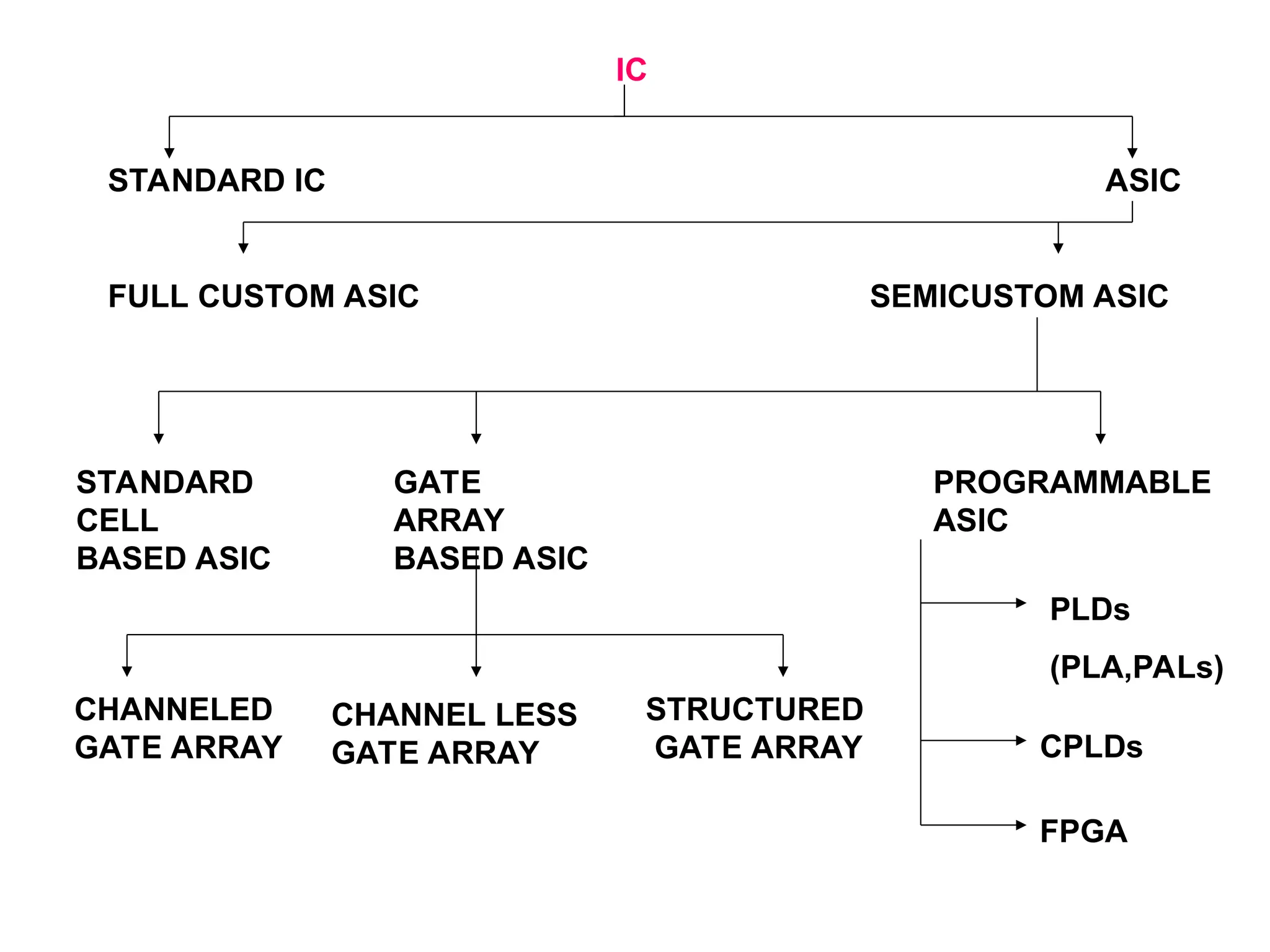
STANDARD IC ASIC
FULLCUSTOM ASIC SEMICUSTOM ASIC
STANDARD
CELL
BASED ASIC
GATE
ARRAY
BASED ASIC
PROGRAMMABLE
ASIC
PLDs
(PLA,PALs)
CPLDs
FPGA
CHANNELED
GATE ARRAY
CHANNEL LESS
GATE ARRAY
STRUCTURED
GATE ARRAY
IC
4.
ASIC vs StandardIC
ASIC vs Standard IC
Standard ICs – ICs sold as Standard Parts
SSI/LSI/ MSI IC such as MUX, Encoder, Memory Chips, or
Microprocessor IC
Application Specific Integrated Circuits (ASIC) –
A Chip for Toy Bear, Auto-Mobile Control Chip, Different
Communication Chips [ GRoT: ICs not Found in Data Book]
Concept Started in 1980s
An IC Customized to a Particular System or Application –
Custom ICs
Digital Designs Became a Matter of Placing of Fewer CICs
or ASICs plus Some Glue Logic
Reduced Cost and Improved Reliability
Application Specific Standard Parts (ASSP) –
Controller Chip for PC or a Modem
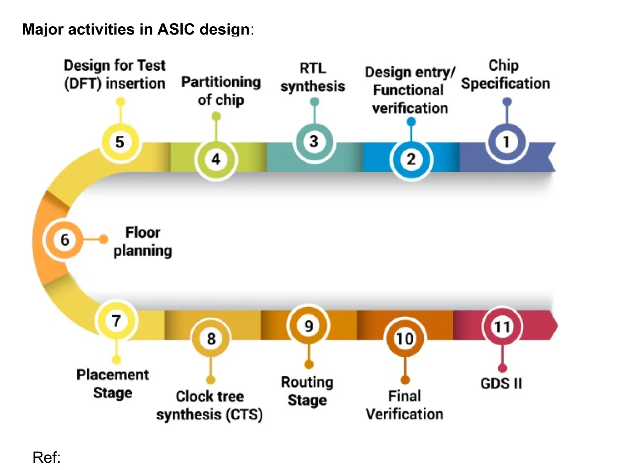
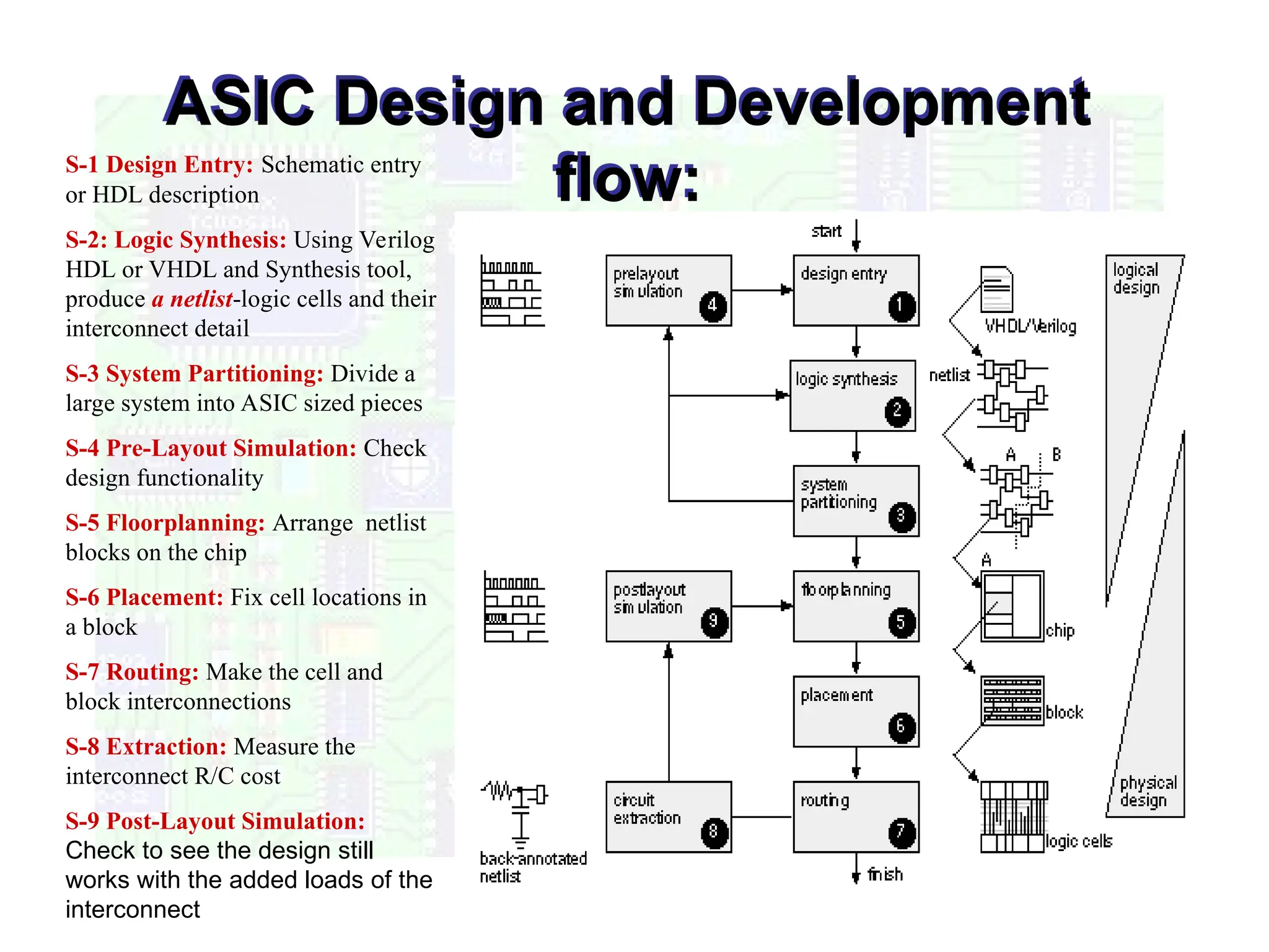
ASIC Design andDevelopment
flow:
S-1 Design Entry: Schematic entry
or HDL description
S-2: Logic Synthesis: Using Verilog
HDL or VHDL and Synthesis tool,
produce a netlist-logic cells and their
interconnect detail
S-3 System Partitioning: Divide a
large system into ASIC sized pieces
S-4 Pre-Layout Simulation: Check
design functionality
S-5 Floorplanning: Arrange netlist
blocks on the chip
S-6 Placement: Fix cell locations in
a block
S-7 Routing: Make the cell and
block interconnections
S-8 Extraction: Measure the
interconnect R/C cost
S-9 Post-Layout Simulation:
Check to see the design still
works with the added loads of the
interconnect
7.
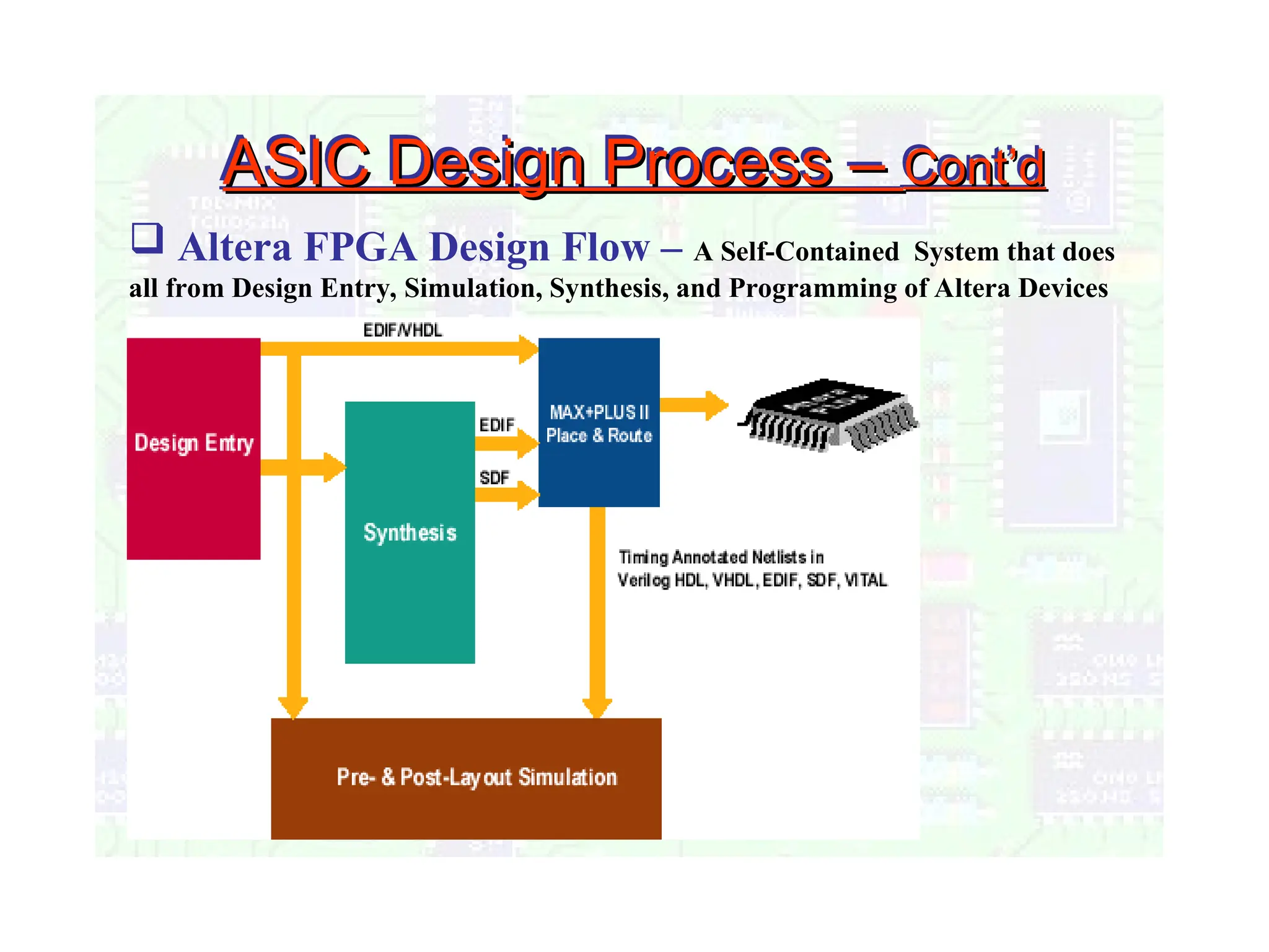
ASIC Design Process–
ASIC Design Process – Cont’d
Cont’d
Altera FPGA Design Flow – A Self-Contained System that does
all from Design Entry, Simulation, Synthesis, and Programming of Altera Devices
8.
ASIC : FULLCUSTOM :Every mask is defined by the designer
SEMICUSTOM: Few masks are defined by designer
Initial manufacturing process is the most complex , time consuming and
expensive part of total manufacturing
an ASIC vendor can usually do this in a couple of weeks ( turn around time)
better performance
More secured design and more compact form
Applicable for both analog and digital
it cannot be replaced if damage occurs
cost is more due to custom design and less productivity
FEATURES OF ASIC
9.
FULL CUSTOM ASIC
Thetime it takes to complete the IC is typically 8 weeks even not includes design
time.
An engineer designs all logic cells, circuits or layouts for one ASIC
Bipolar technology has historically been used for precision analog functions
CMOS also used because it is easier to design Analog and Digital chips with
better performance
The entire mask design is done a new without use of any library. However
development cost of such design style is becoming prohibitively high.
Bipolar : In all integrated circuits the matching of component characteristics
between chips is very poor, while the matching of characteristics between
components on the same chip is excellent.
For many analog designs the close matching of transistors is crucial to circuit
operation. For these circuit designs pairs of transistors are used , located adjacent
to each other. Device physics dictates the pair of bipolar transistors will always
match more precisely than CMOS transistors of comparable size.
10.
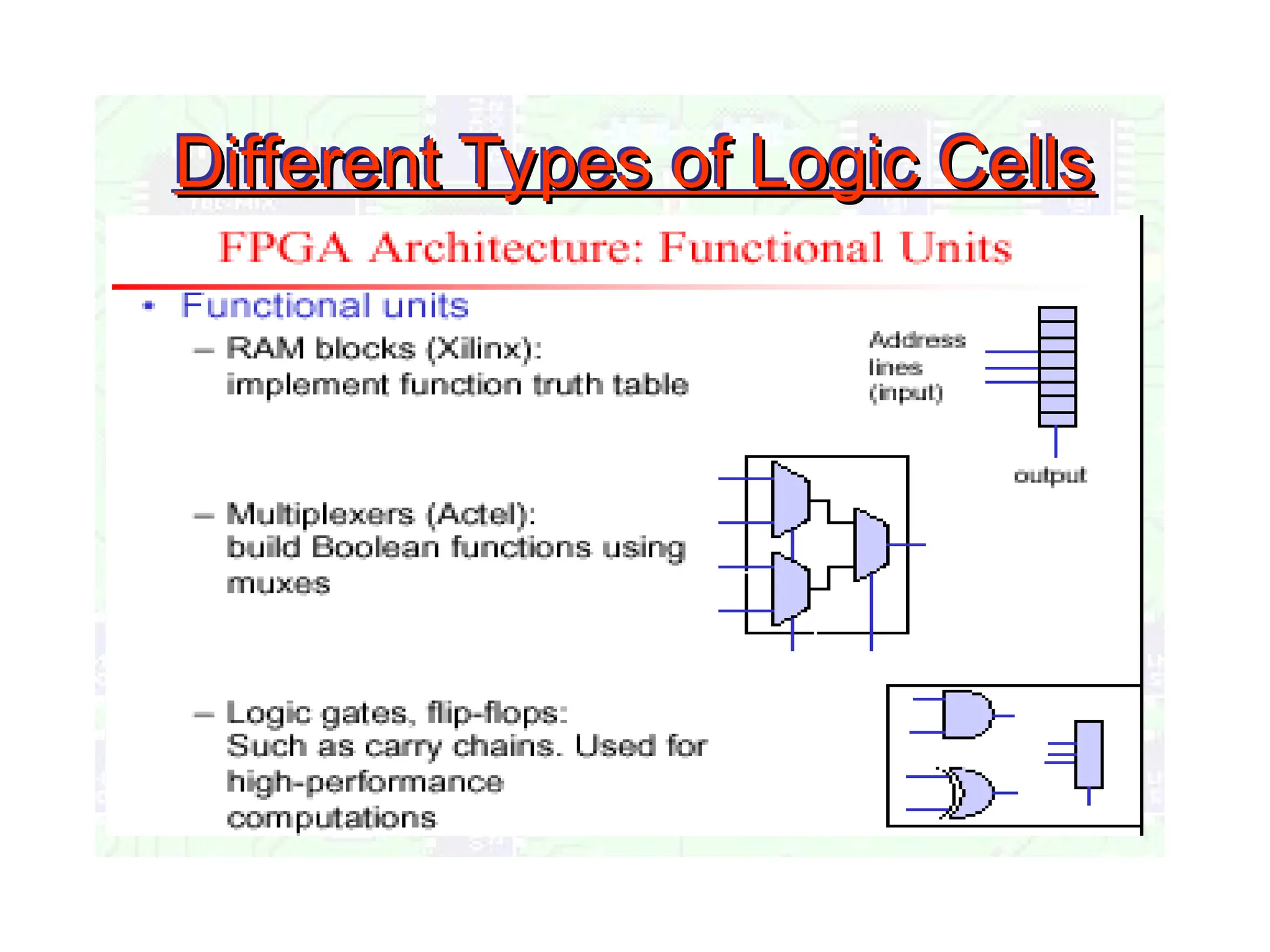
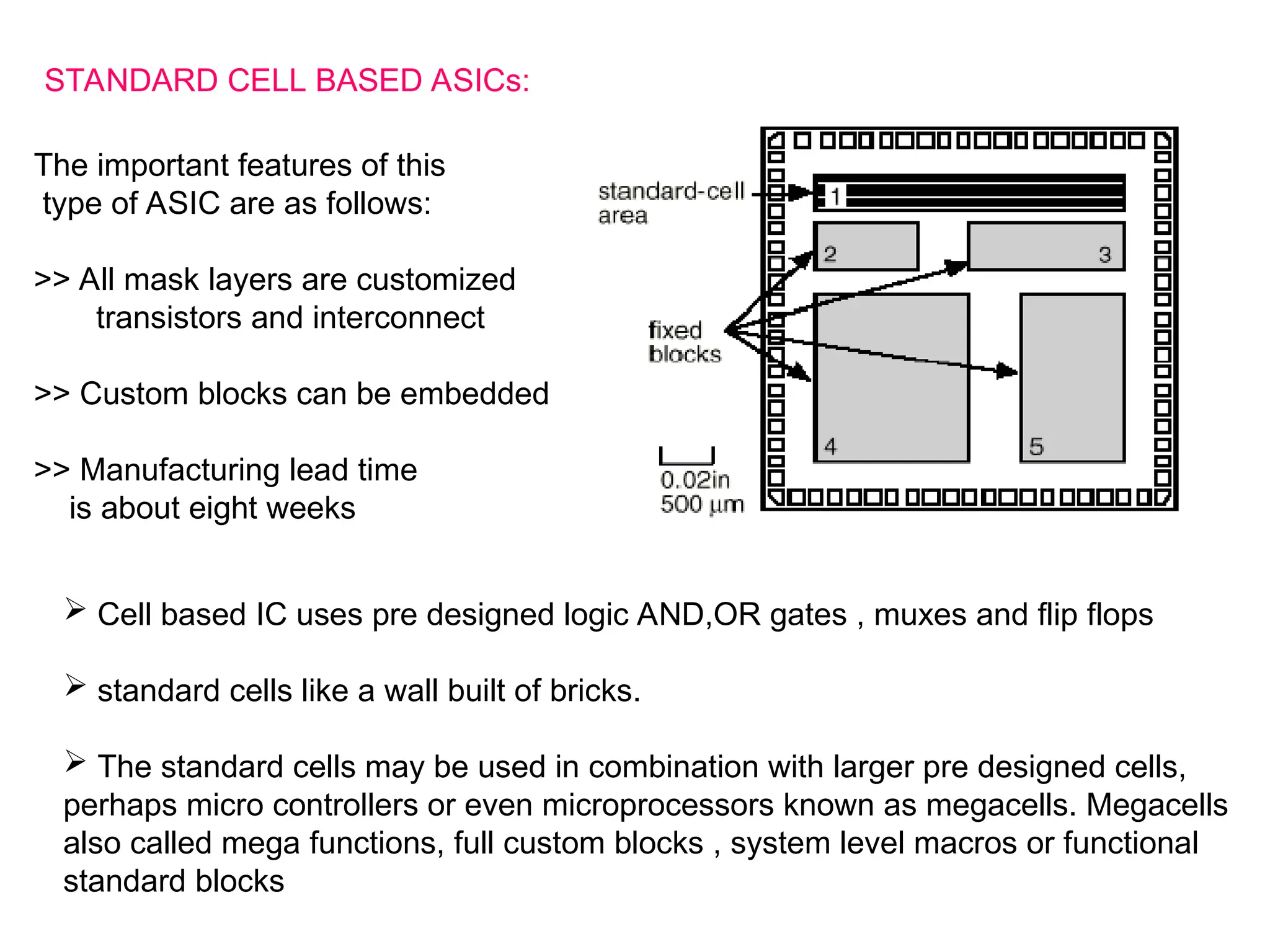
STANDARD CELL BASEDASICs:
The important features of this
type of ASIC are as follows:
>> All mask layers are customized
transistors and interconnect
>> Custom blocks can be embedded
>> Manufacturing lead time
is about eight weeks
Cell based IC uses pre designed logic AND,OR gates , muxes and flip flops
standard cells like a wall built of bricks.
The standard cells may be used in combination with larger pre designed cells,
perhaps micro controllers or even microprocessors known as megacells. Megacells
also called mega functions, full custom blocks , system level macros or functional
standard blocks
11.
However, thestandard cells can be placed anywhere on the silicon;this means
that all the mask layers of a CBIC are customized and are unique to a particular
customer.
The advantage of CBICs is that designers save time, money, and reduce risk
by using a pre designed, pre tested and pre characterized standard library .
The disadvantages are the time or expense of designing or buying the standard
cell library and the time needed to fabricate all layers of the ASIC for each new
design
power and ground lines run parallel to the upper and lower boundaries of the
cell, thus, neighboring cells share a common power and ground bus.
in many VLSI chips , such as microprocessors and DSP chips , standard cell
based design used to implement complex control logic modules.
characterization of each cell based on 1.Delay Vs CL
2. Circuit simulation model
3. timing and fault simulations
4. cell data for place and route
12.
GATE ARRAY BASEDASIC:
Both cell based and gate array ASICs use predefined cells, but there is a
difference- we can change the transistor sizes in a standard cell to optimize speed
and performance, but the device sizes in a gate array are fixed.
Standard cells and gate array libraries may contain both combinational and
sequential logic cells with different combinations of reset, preset and clocking
options. The ASIC library company provides designers with a data book or
electronic form with all functional descriptions and timing information for each
library element.
If PLAs are used, such logic functions would require more area and delay time.
Also design time with gate arrays is shorter than standard cell design.
In a gate-array-based ASIC the transistors are predefined on the silicon wafer.
The predefined pattern of transistors on a gate array is the base array, and the
smallest element that is replicated to make the base array is the base cell
(sometimes called a primitive cell).
13.
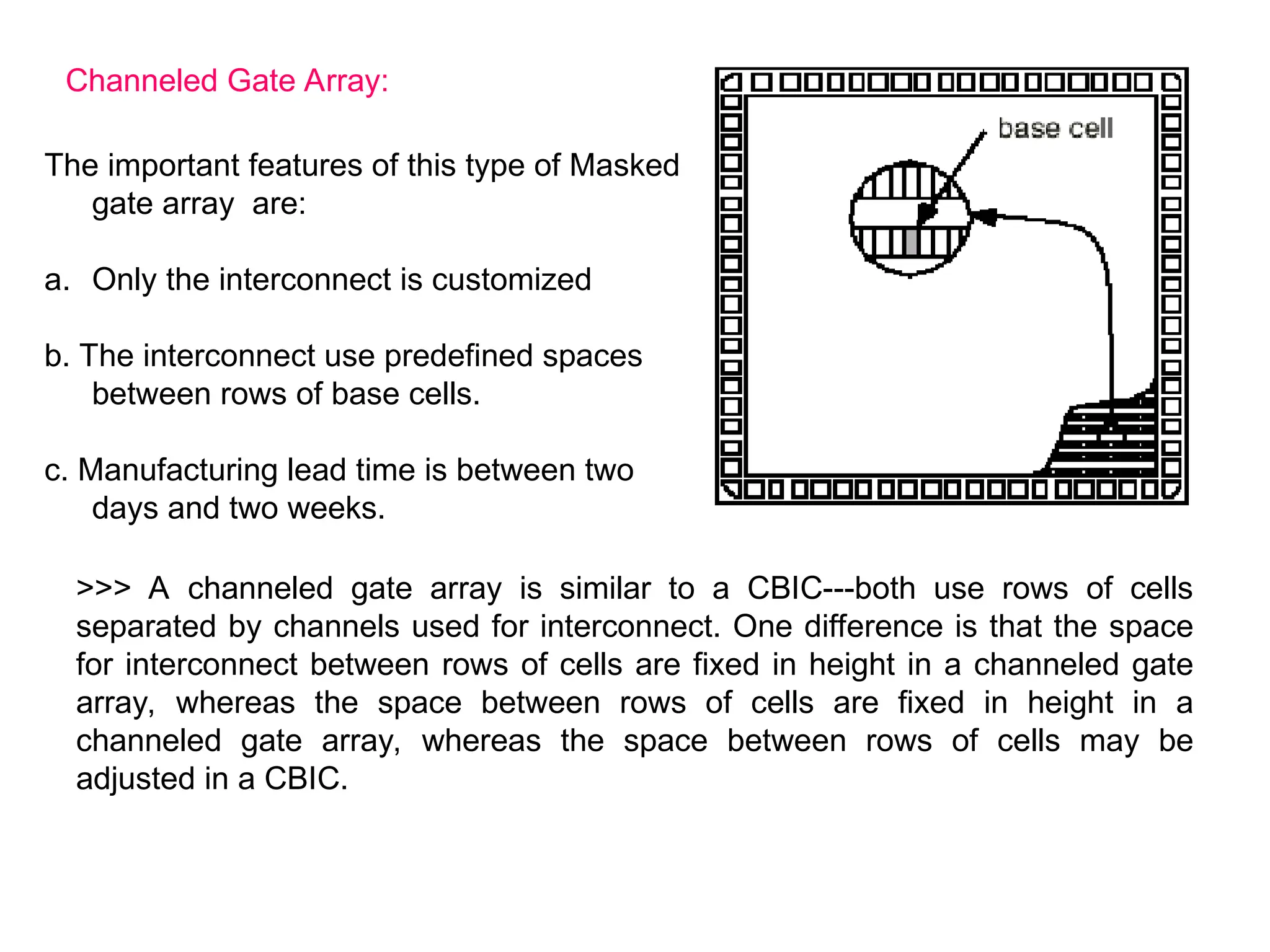
Channeled Gate Array:
Theimportant features of this type of Masked
gate array are:
a. Only the interconnect is customized
b. The interconnect use predefined spaces
between rows of base cells.
c. Manufacturing lead time is between two
days and two weeks.
>>> A channeled gate array is similar to a CBIC---both use rows of cells
separated by channels used for interconnect. One difference is that the space
for interconnect between rows of cells are fixed in height in a channeled gate
array, whereas the space between rows of cells are fixed in height in a
channeled gate array, whereas the space between rows of cells may be
adjusted in a CBIC.
14.
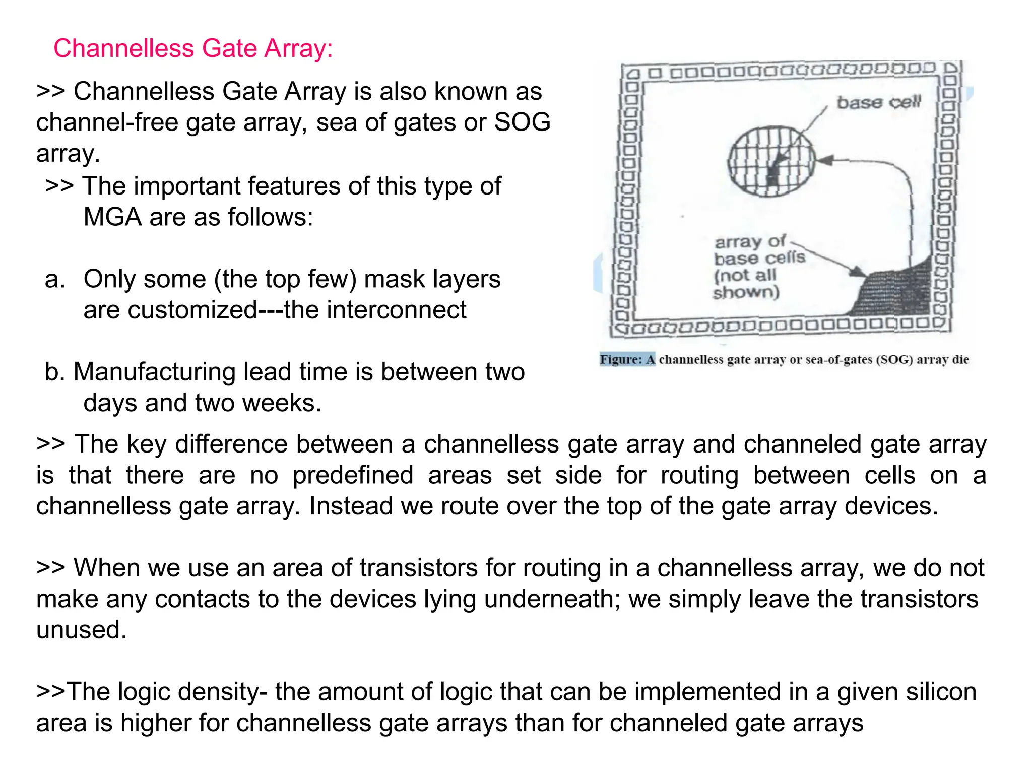
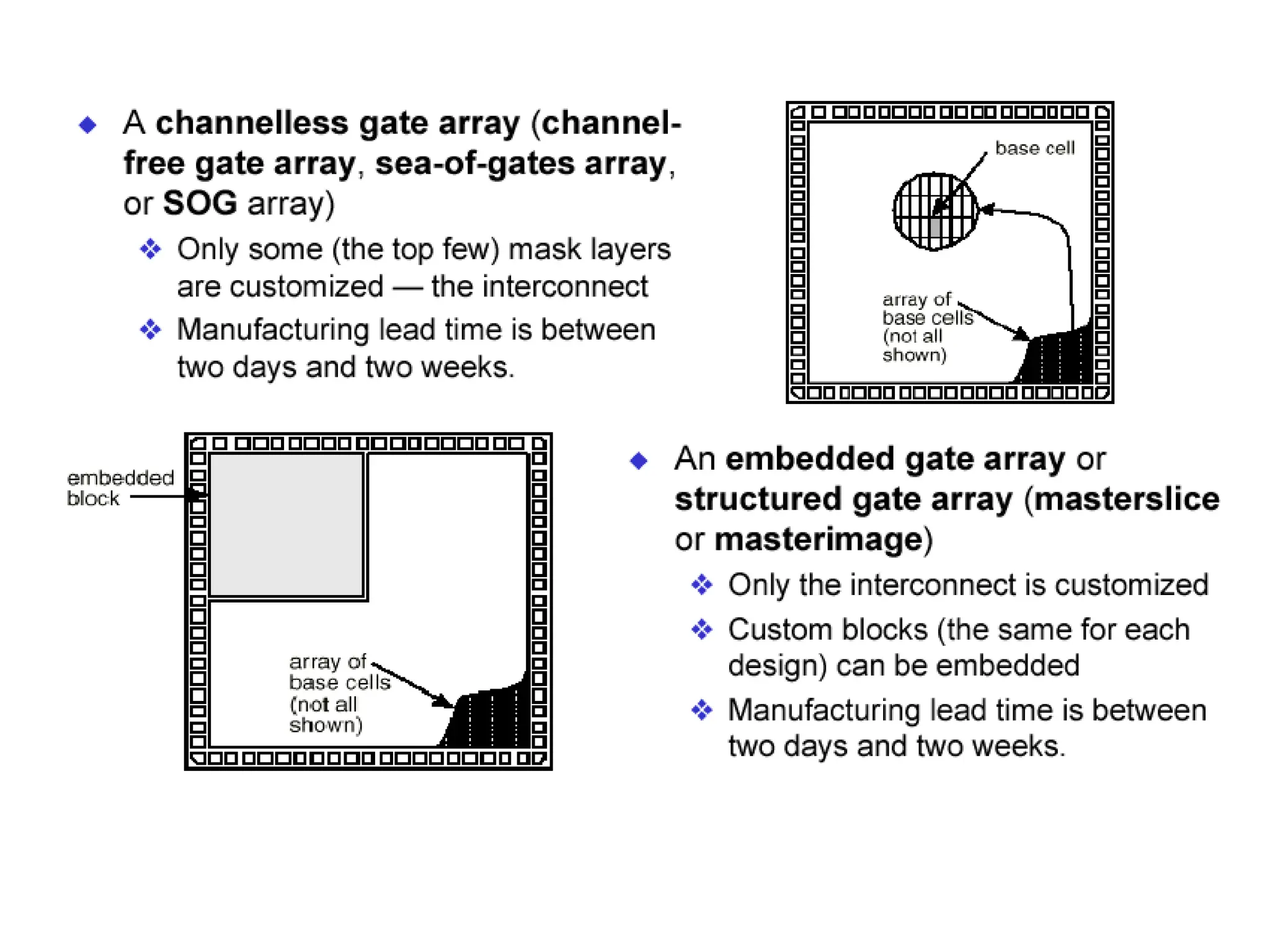
Channelless Gate Array:
>>Channelless Gate Array is also known as
channel-free gate array, sea of gates or SOG
array.
>> The important features of this type of
MGA are as follows:
a. Only some (the top few) mask layers
are customized---the interconnect
b. Manufacturing lead time is between two
days and two weeks.
>> The key difference between a channelless gate array and channeled gate array
is that there are no predefined areas set side for routing between cells on a
channelless gate array. Instead we route over the top of the gate array devices.
>> When we use an area of transistors for routing in a channelless array, we do not
make any contacts to the devices lying underneath; we simply leave the transistors
unused.
>>The logic density- the amount of logic that can be implemented in a given silicon
area is higher for channelless gate arrays than for channeled gate arrays
15.
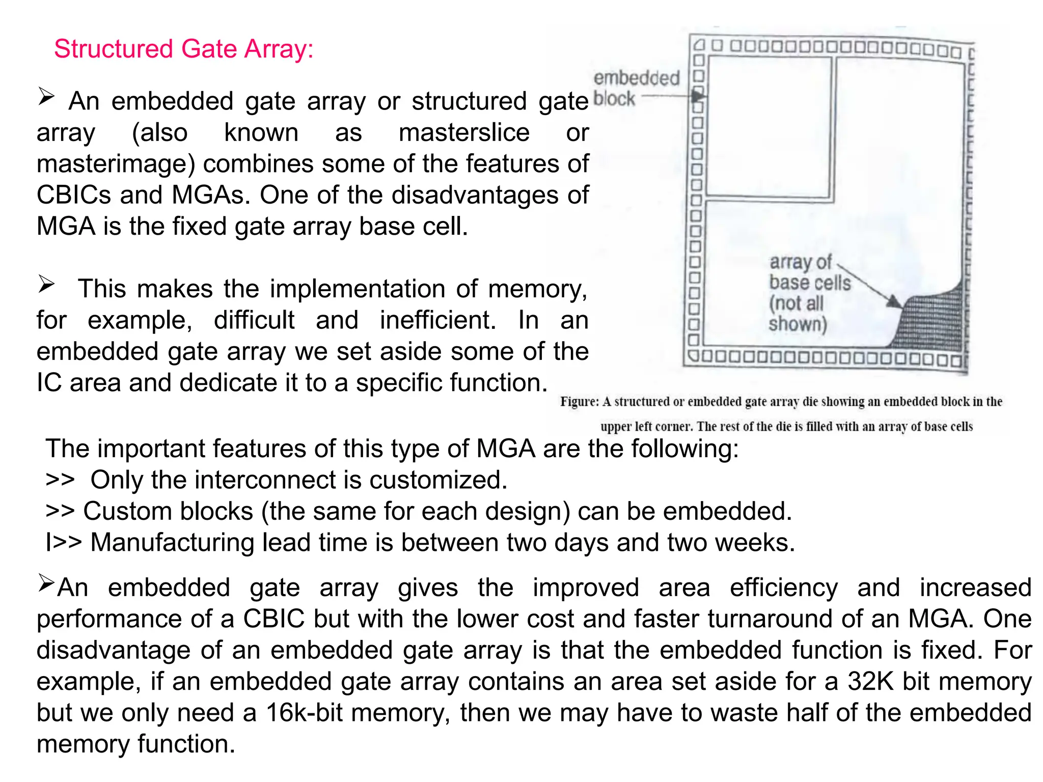
Structured Gate Array:
An embedded gate array or structured gate
array (also known as masterslice or
masterimage) combines some of the features of
CBICs and MGAs. One of the disadvantages of
MGA is the fixed gate array base cell.
This makes the implementation of memory,
for example, difficult and inefficient. In an
embedded gate array we set aside some of the
IC area and dedicate it to a specific function.
The important features of this type of MGA are the following:
>> Only the interconnect is customized.
>> Custom blocks (the same for each design) can be embedded.
I>> Manufacturing lead time is between two days and two weeks.
An embedded gate array gives the improved area efficiency and increased
performance of a CBIC but with the lower cost and faster turnaround of an MGA. One
disadvantage of an embedded gate array is that the embedded function is fixed. For
example, if an embedded gate array contains an area set aside for a 32K bit memory
but we only need a 16k-bit memory, then we may have to waste half of the embedded
memory function.
17.
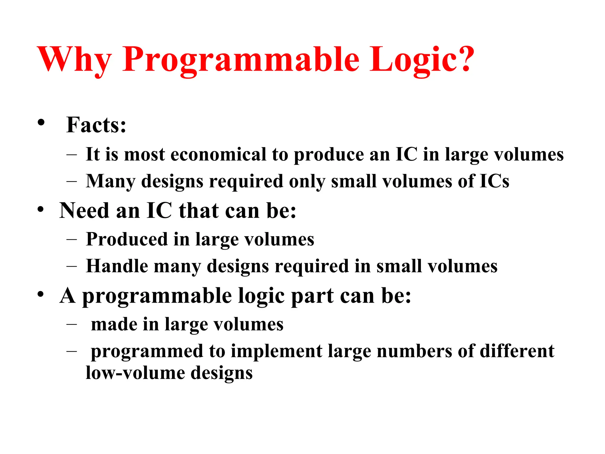
Why Programmable Logic?
•Facts:
– It is most economical to produce an IC in large volumes
– Many designs required only small volumes of ICs
• Need an IC that can be:
– Produced in large volumes
– Handle many designs required in small volumes
• A programmable logic part can be:
– made in large volumes
– programmed to implement large numbers of different
low-volume designs
18.
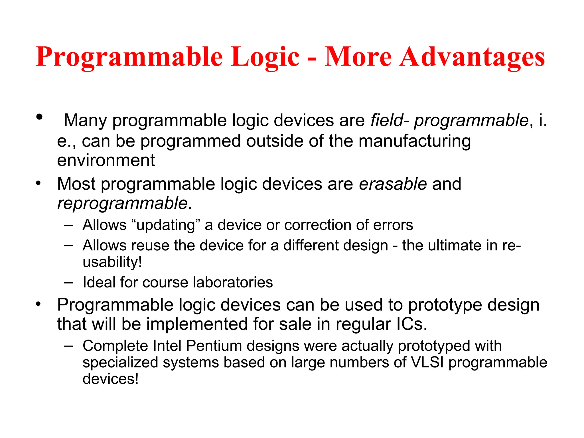
Programmable Logic -More Advantages
• Many programmable logic devices are field- programmable, i.
e., can be programmed outside of the manufacturing
environment
• Most programmable logic devices are erasable and
reprogrammable.
– Allows “updating” a device or correction of errors
– Allows reuse the device for a different design - the ultimate in re-
usability!
– Ideal for course laboratories
• Programmable logic devices can be used to prototype design
that will be implemented for sale in regular ICs.
– Complete Intel Pentium designs were actually prototyped with
specialized systems based on large numbers of VLSI programmable
devices!
19.
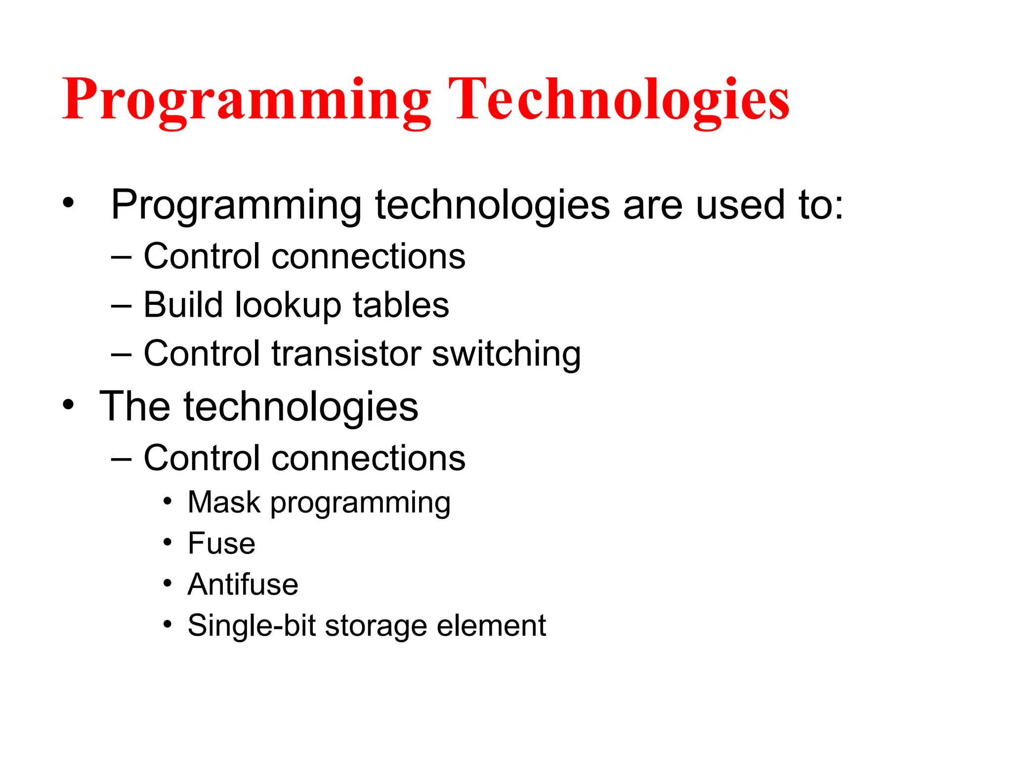
Programming Technologies
• Programmingtechnologies are used to:
– Control connections
– Build lookup tables
– Control transistor switching
• The technologies
– Control connections
• Mask programming
• Fuse
• Antifuse
• Single-bit storage element
20.
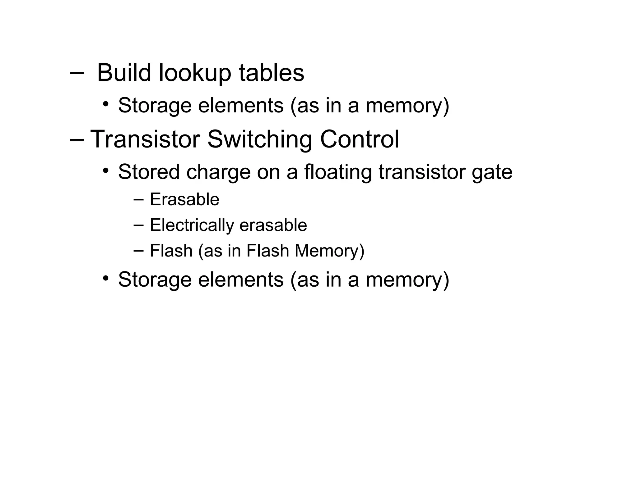
– Build lookuptables
• Storage elements (as in a memory)
– Transistor Switching Control
• Stored charge on a floating transistor gate
– Erasable
– Electrically erasable
– Flash (as in Flash Memory)
• Storage elements (as in a memory)
21.
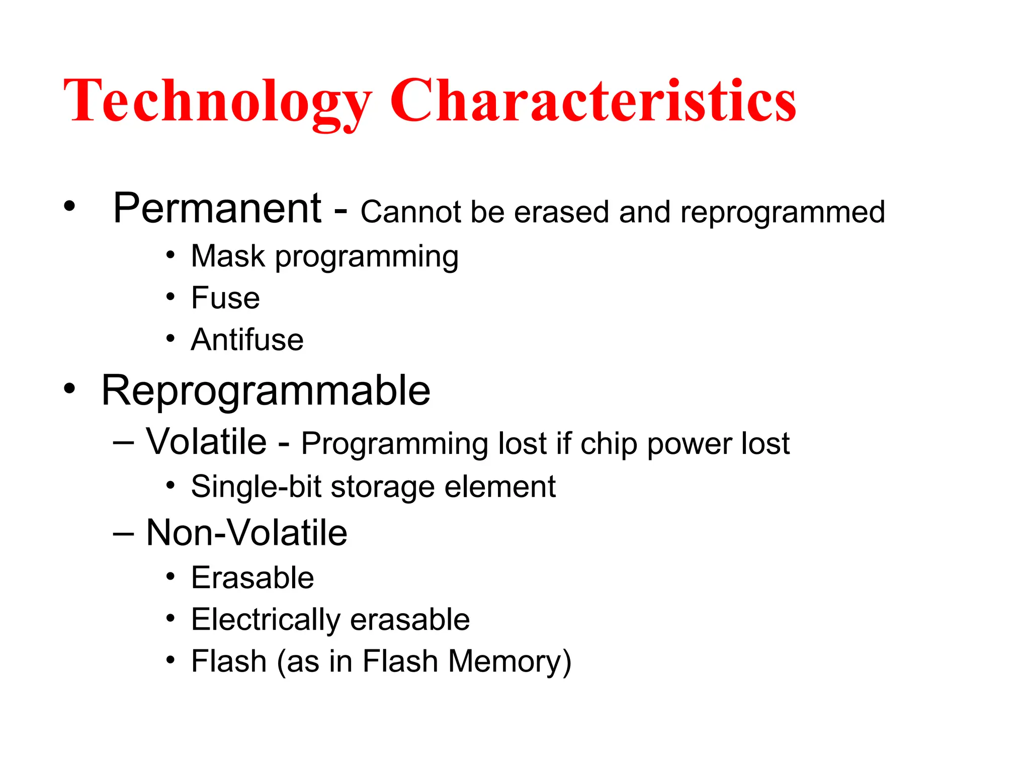
Technology Characteristics
• Permanent- Cannot be erased and reprogrammed
• Mask programming
• Fuse
• Antifuse
• Reprogrammable
– Volatile - Programming lost if chip power lost
• Single-bit storage element
– Non-Volatile
• Erasable
• Electrically erasable
• Flash (as in Flash Memory)
22.
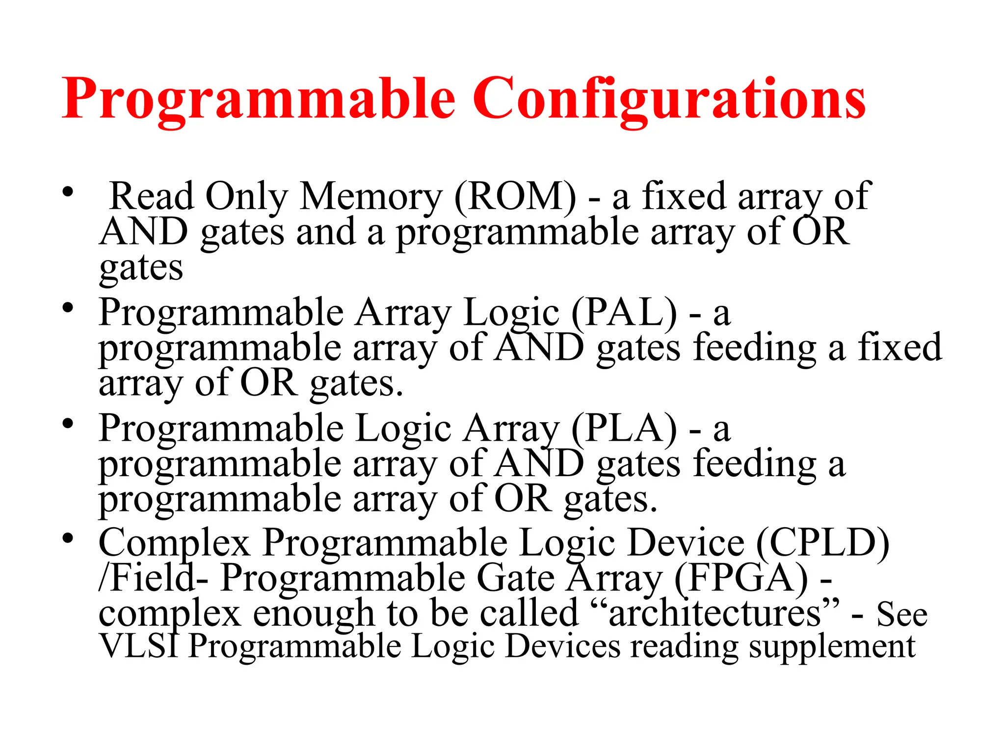
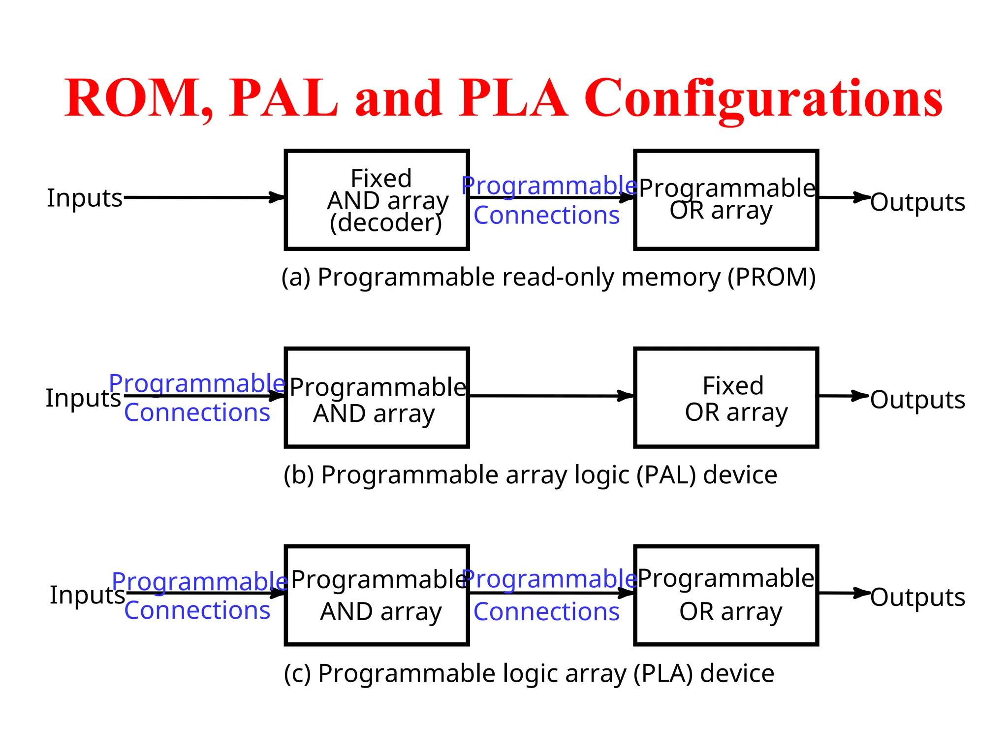
Programmable Configurations
• ReadOnly Memory (ROM) - a fixed array of
AND gates and a programmable array of OR
gates
• Programmable Array Logic (PAL) - a
programmable array of AND gates feeding a fixed
array of OR gates.
• Programmable Logic Array (PLA) - a
programmable array of AND gates feeding a
programmable array of OR gates.
• Complex Programmable Logic Device (CPLD)
/Field- Programmable Gate Array (FPGA) -
complex enough to be called “architectures” - See
VLSI Programmable Logic Devices reading supplement
23.
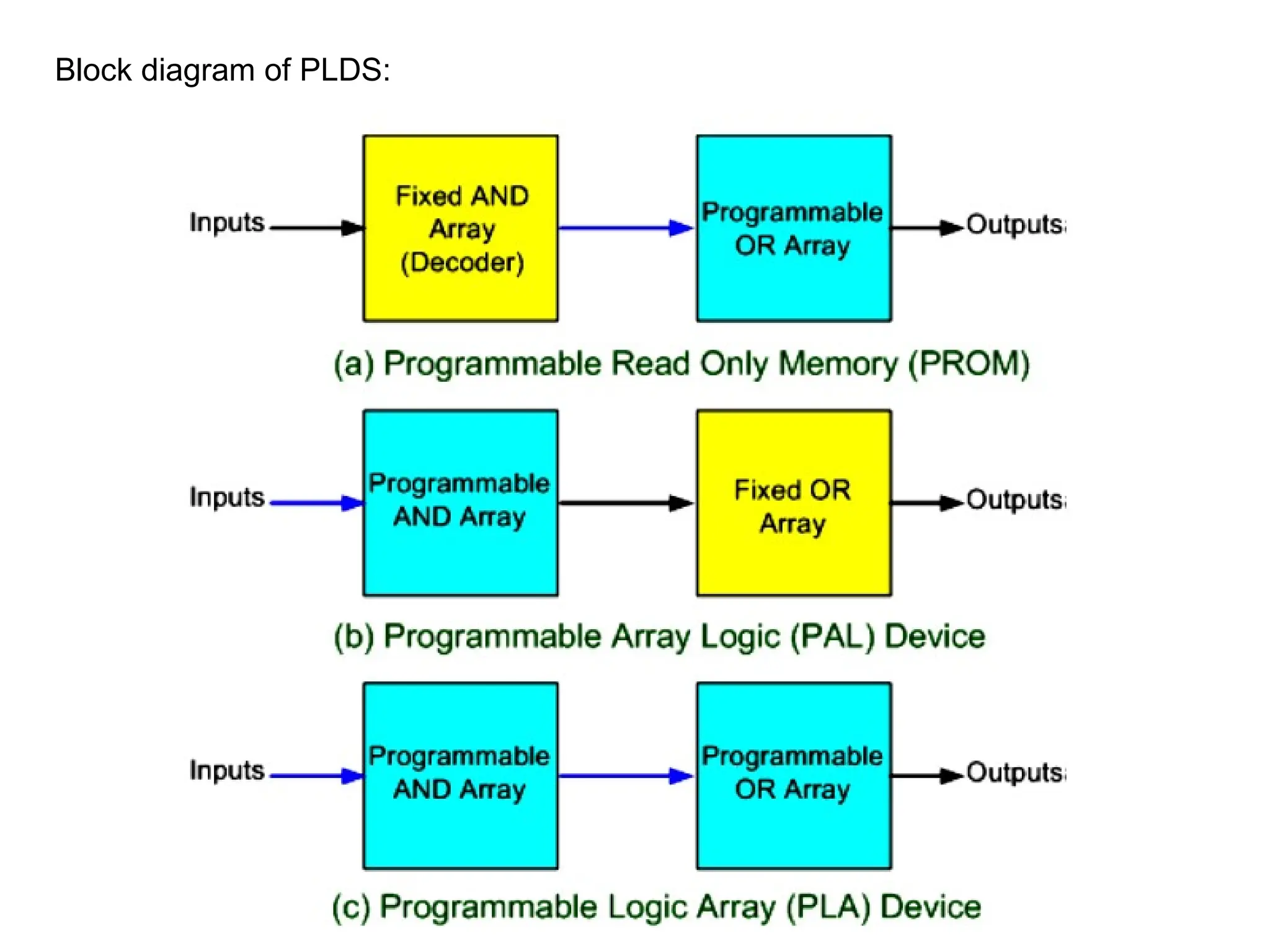
ROM, PAL andPLA Configurations
(a) Programmable read-only memory (PROM)
Inputs
Fixed
AND array
(decoder)
Programmable
OR array Outputs
Programmable
Connections
(b) Programmable array logic (PAL) device
Inputs Programmable
AND array
Fixed
OR array Outputs
Programmable
Connections
(c) Programmable logic array (PLA) device
Inputs
Programmable
OR array
Outputs
Programmable
Connections
Programmable
Connections
Programmable
AND array
24.
24
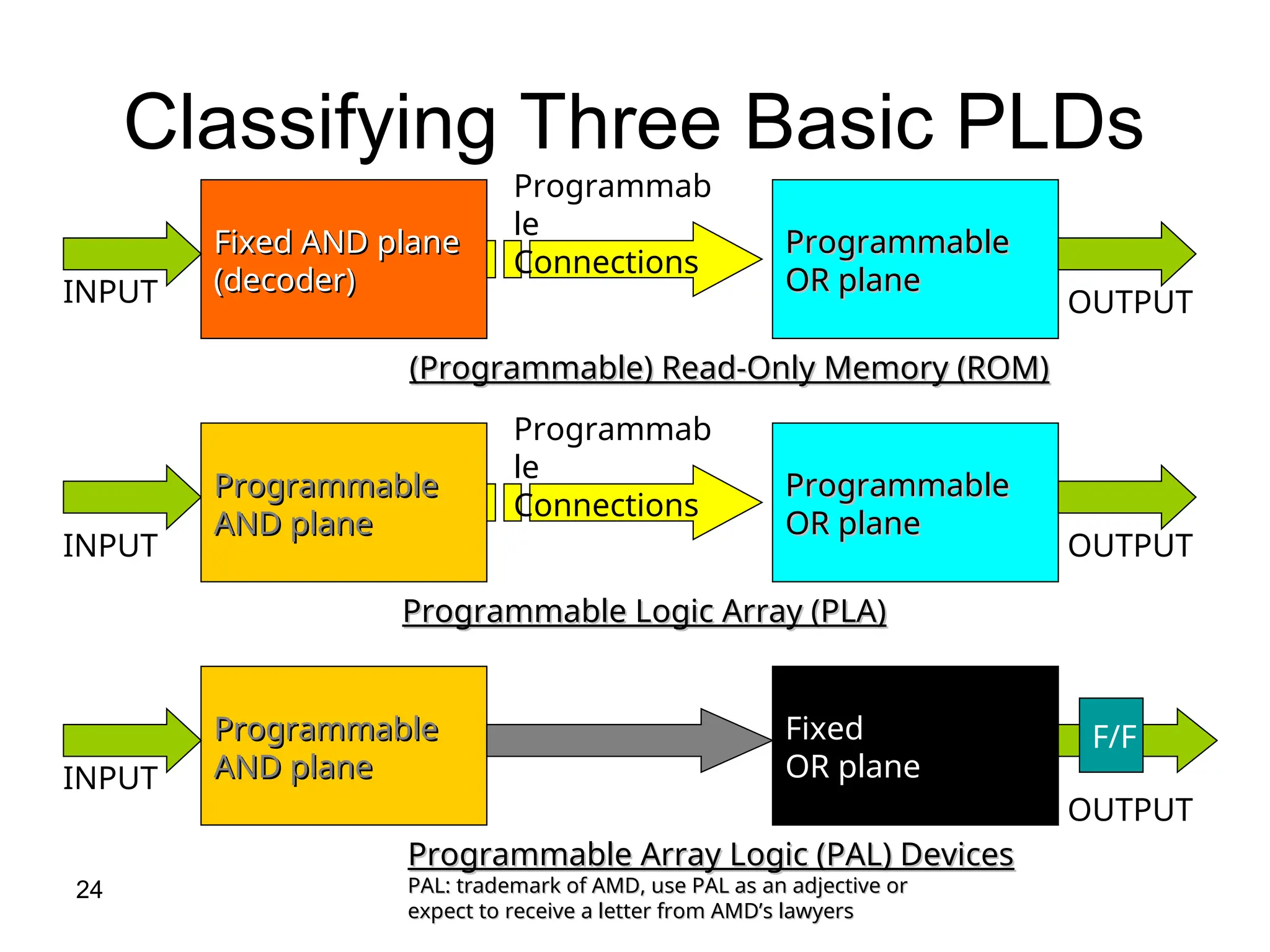
Classifying Three BasicPLDs
Fixed AND plane
Fixed AND plane
(decoder)
(decoder)
Programmable
Programmable
OR plane
OR plane
Programmab
le
Connections
(Programmable) Read-Only Memory (ROM)
(Programmable) Read-Only Memory (ROM)
INPUT OUTPUT
Programmable
Programmable
OR plane
OR plane
Programmab
le
Connections
Programmable Logic Array (PLA)
Programmable Logic Array (PLA)
Programmable
Programmable
AND plane
AND plane
INPUT OUTPUT
Programmable
Programmable
AND plane
AND plane
Fixed
Fixed
OR plane
OR plane
Programmable Array Logic (PAL) Devices
Programmable Array Logic (PAL) Devices
PAL: trademark of AMD, use PAL as an adjective or
PAL: trademark of AMD, use PAL as an adjective or
expect to receive a letter from AMD’s lawyers
expect to receive a letter from AMD’s lawyers
INPUT
OUTPUT
F/F
25.
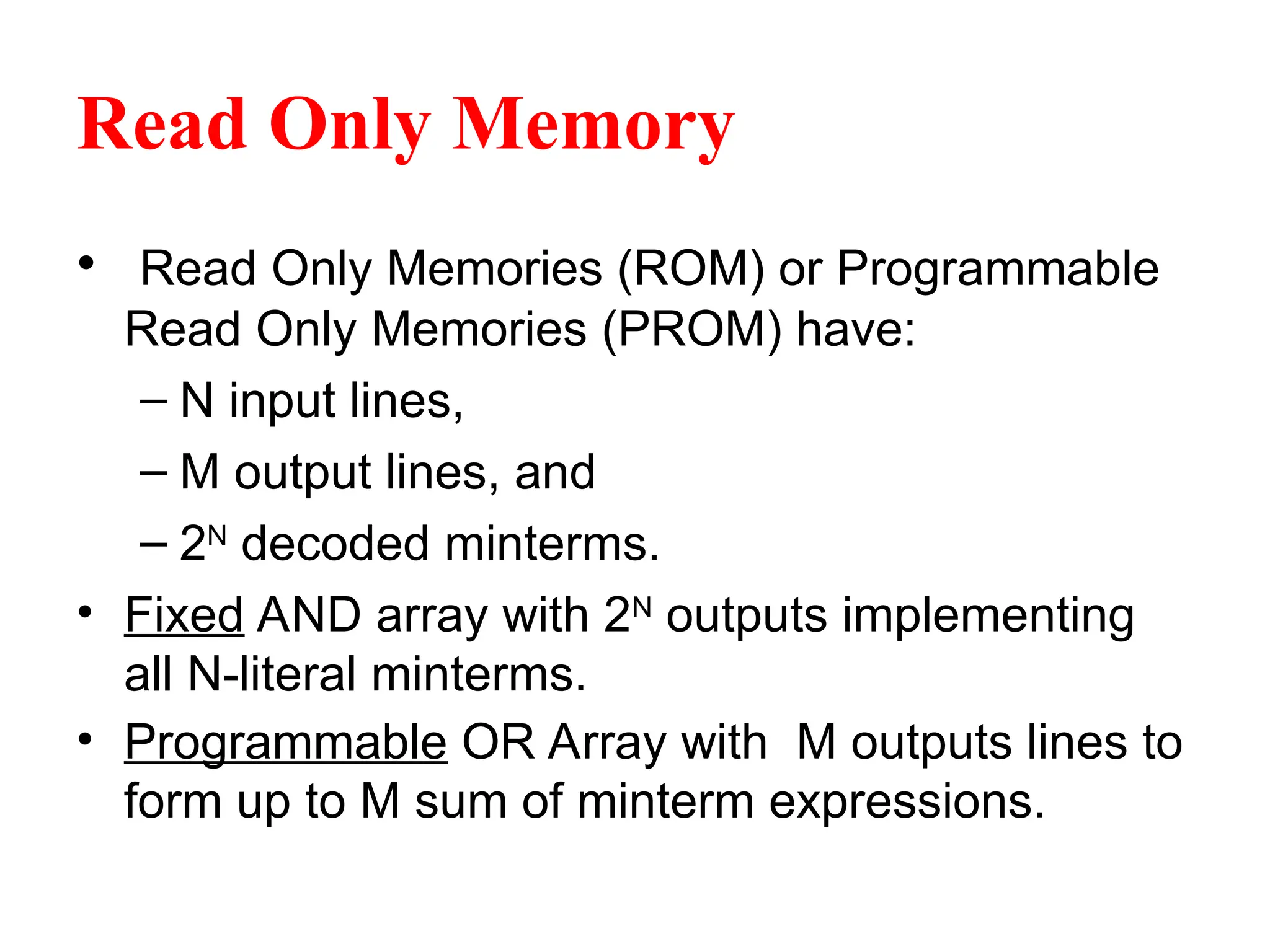
Read Only Memory
•Read Only Memories (ROM) or Programmable
Read Only Memories (PROM) have:
– N input lines,
– M output lines, and
– 2N
decoded minterms.
• Fixed AND array with 2N
outputs implementing
all N-literal minterms.
• Programmable OR Array with M outputs lines to
form up to M sum of minterm expressions.
26.
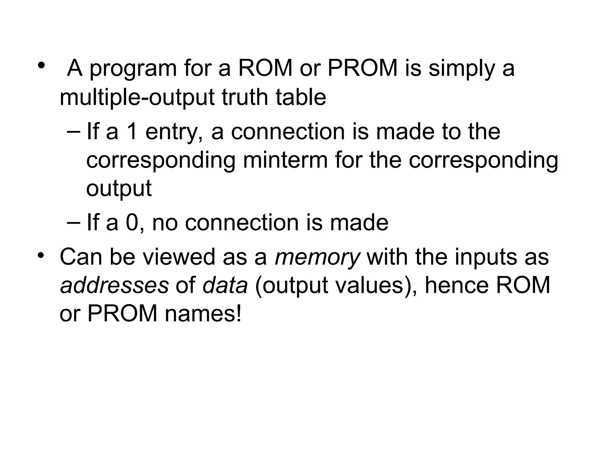
• A programfor a ROM or PROM is simply a
multiple-output truth table
– If a 1 entry, a connection is made to the
corresponding minterm for the corresponding
output
– If a 0, no connection is made
• Can be viewed as a memory with the inputs as
addresses of data (output values), hence ROM
or PROM names!
27.
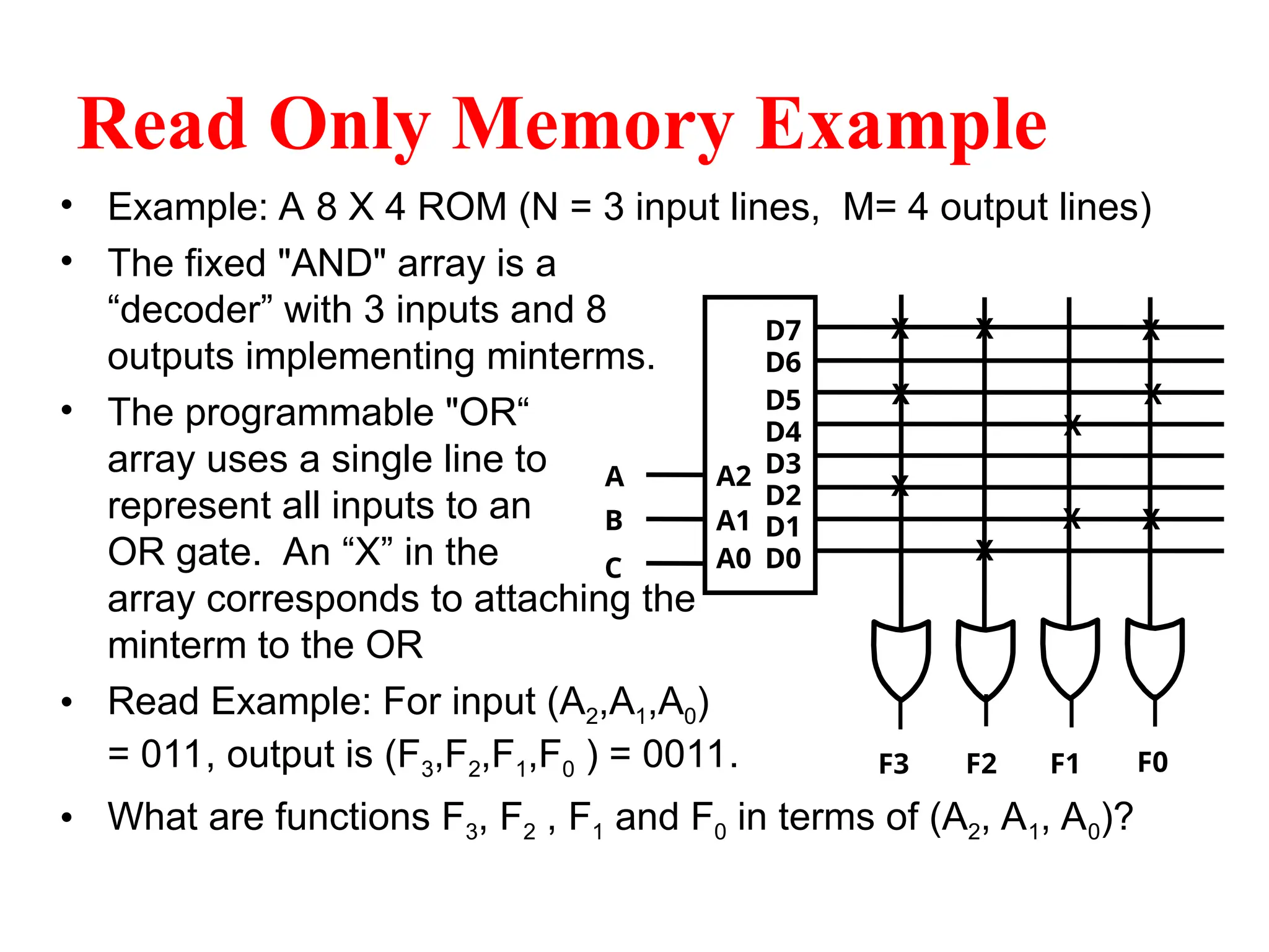
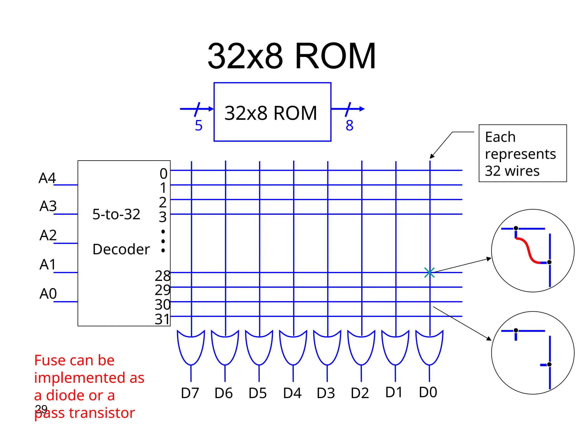
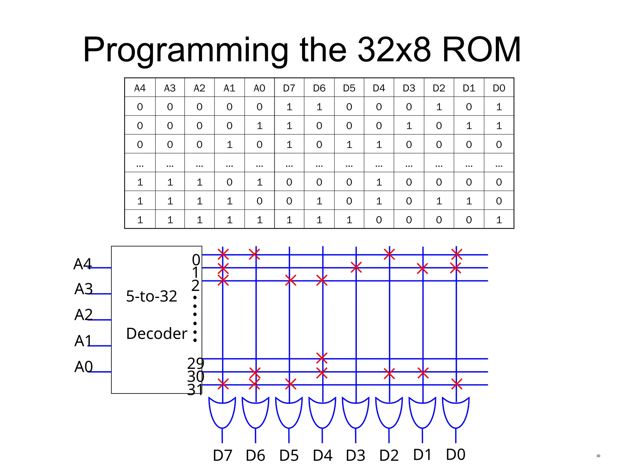
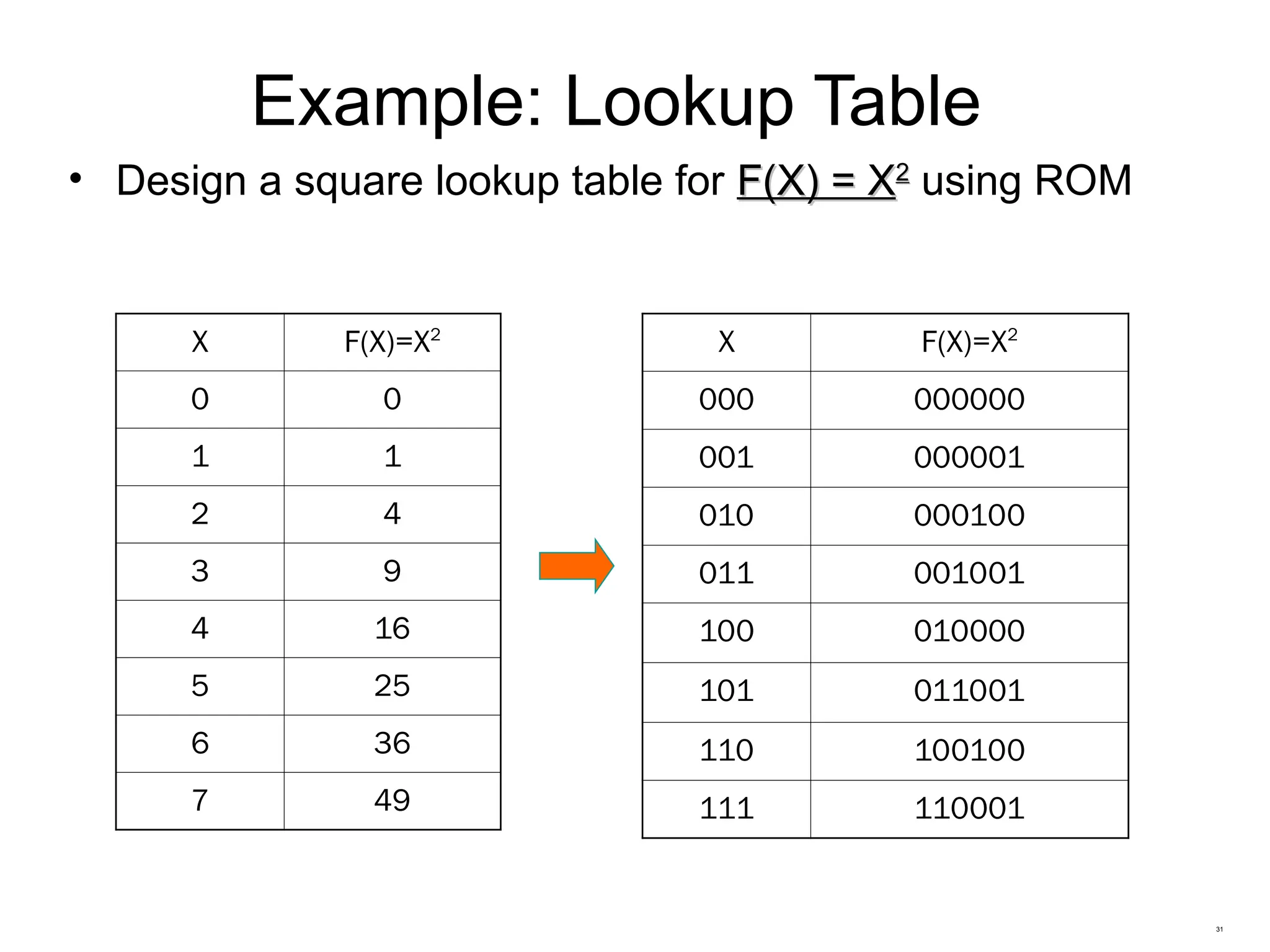
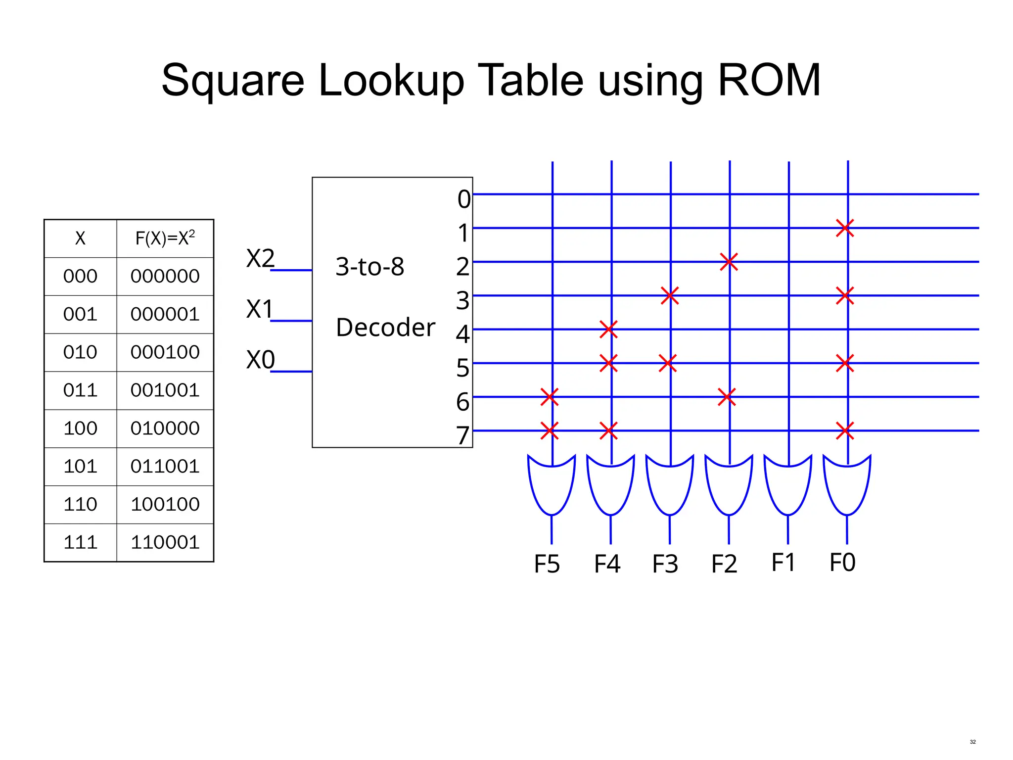
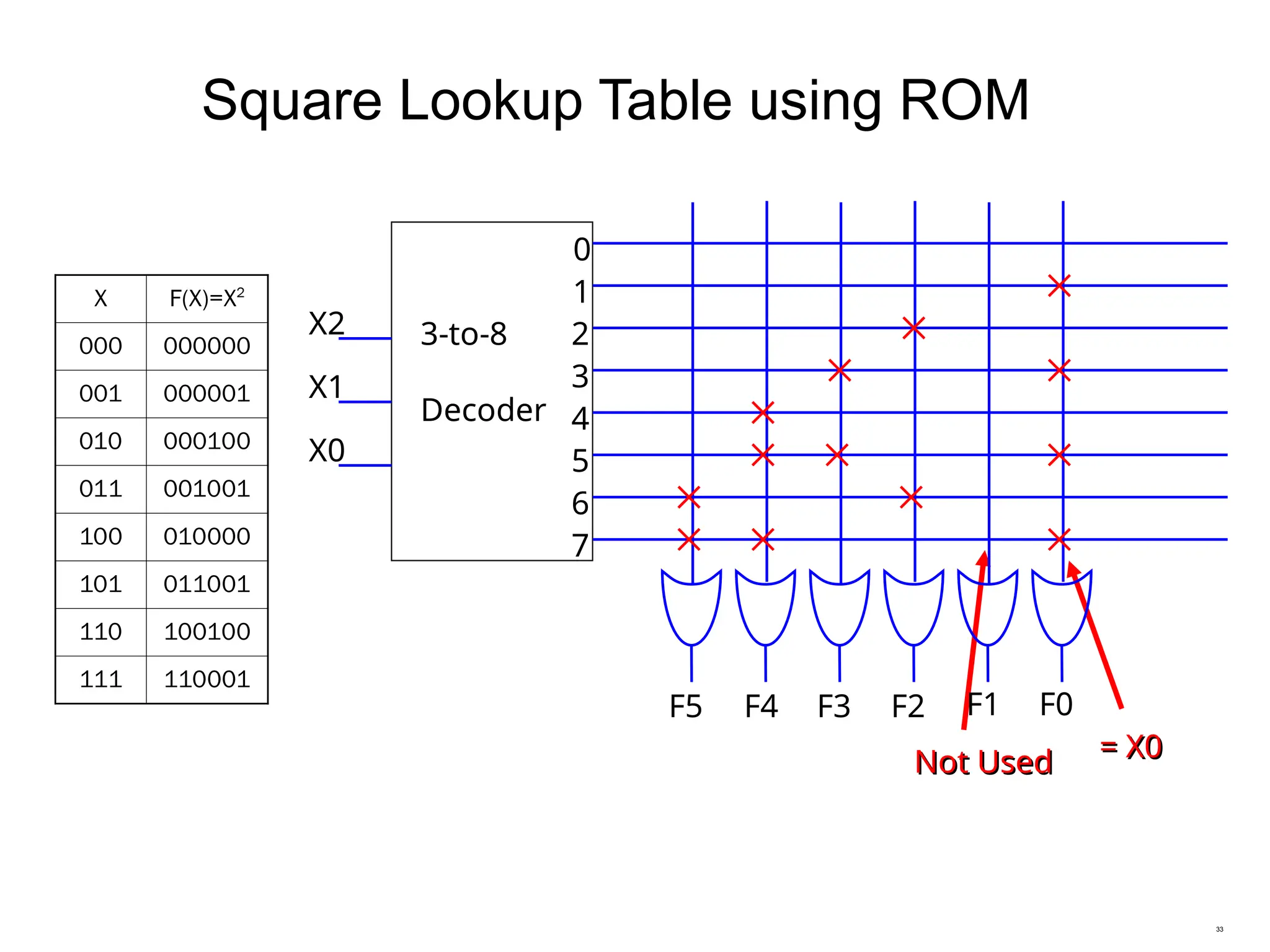
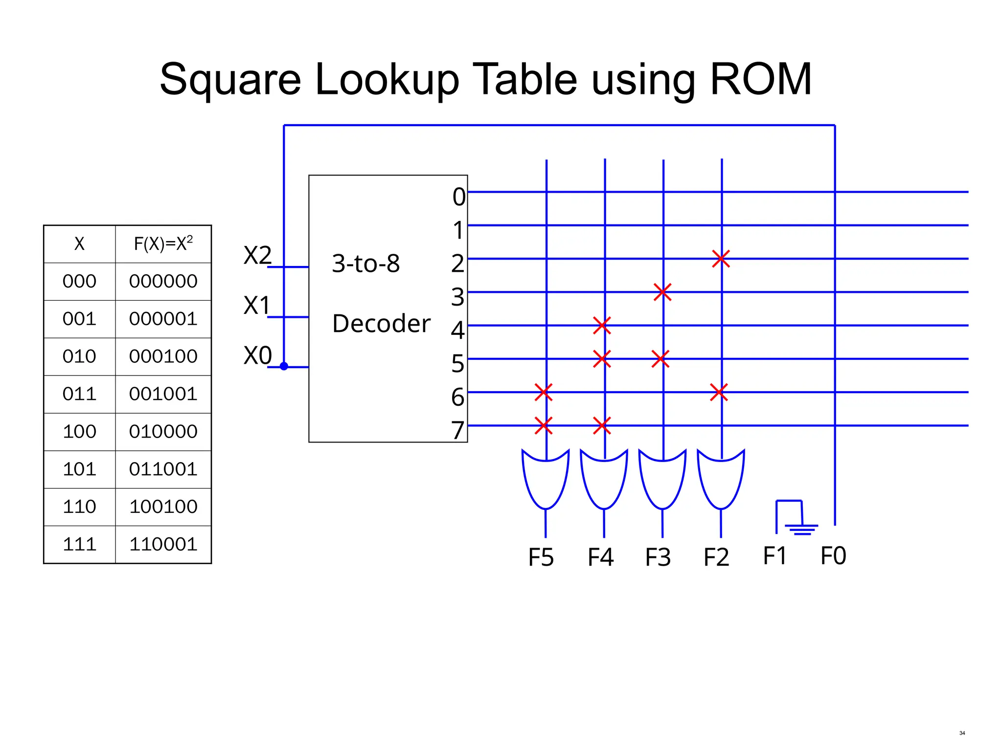
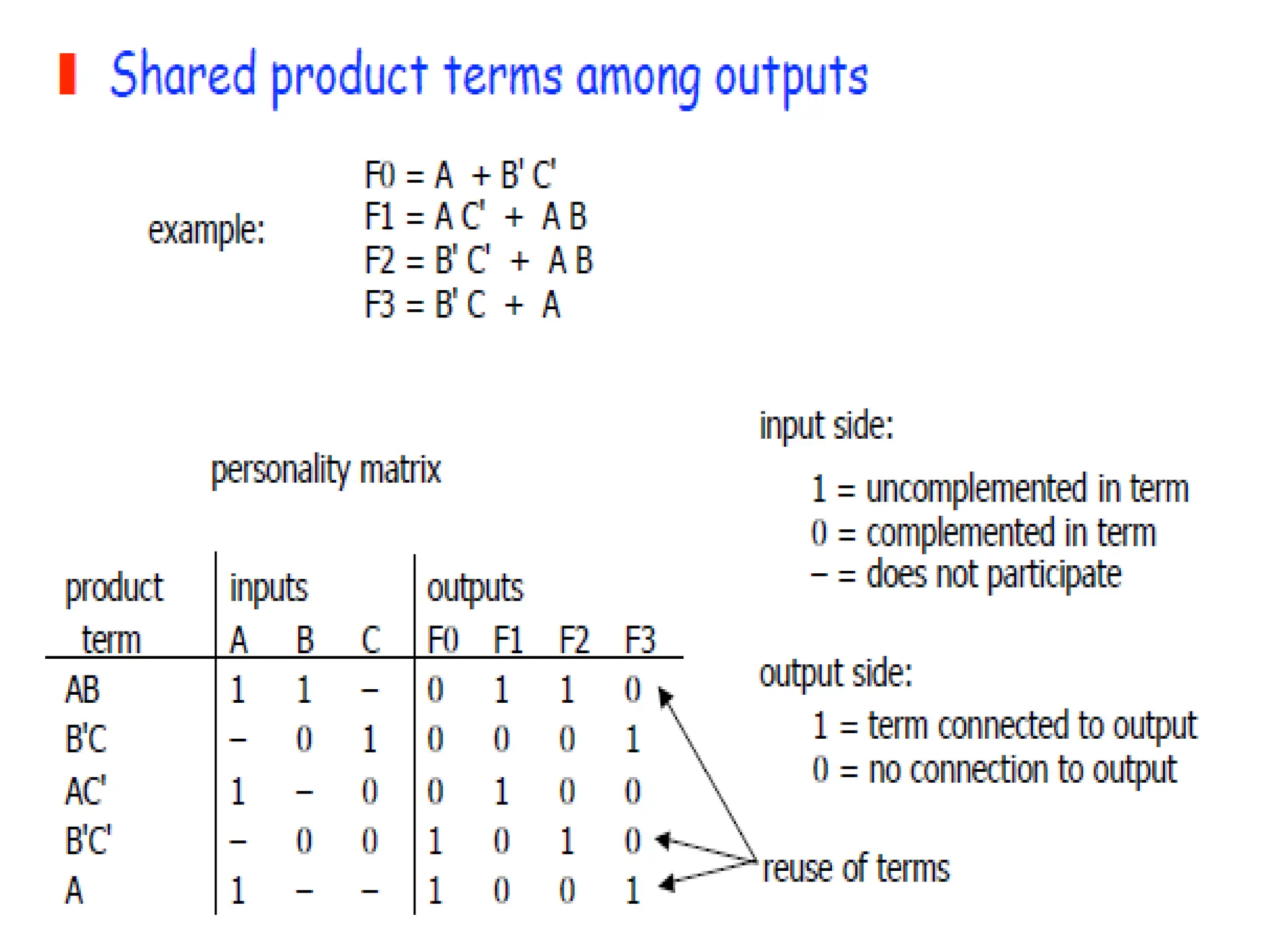
Read Only MemoryExample
• Example: A 8 X 4 ROM (N = 3 input lines, M= 4 output lines)
• The fixed "AND" array is a
“decoder” with 3 inputs and 8
outputs implementing minterms.
• The programmable "OR“
array uses a single line to
represent all inputs to an
OR gate. An “X” in the
array corresponds to attaching the
minterm to the OR
• Read Example: For input (A2,A1,A0)
= 011, output is (F3,F2,F1,F0 ) = 0011.
• What are functions F3, F2 , F1 and F0 in terms of (A2, A1, A0)?
D7
D6
D5
D4
D3
D2
D1
D0
A2
A1
A0
A
B
C
F0
F1
F2
F3
X X
X
X
X
X
X
X
X
X
28.
28
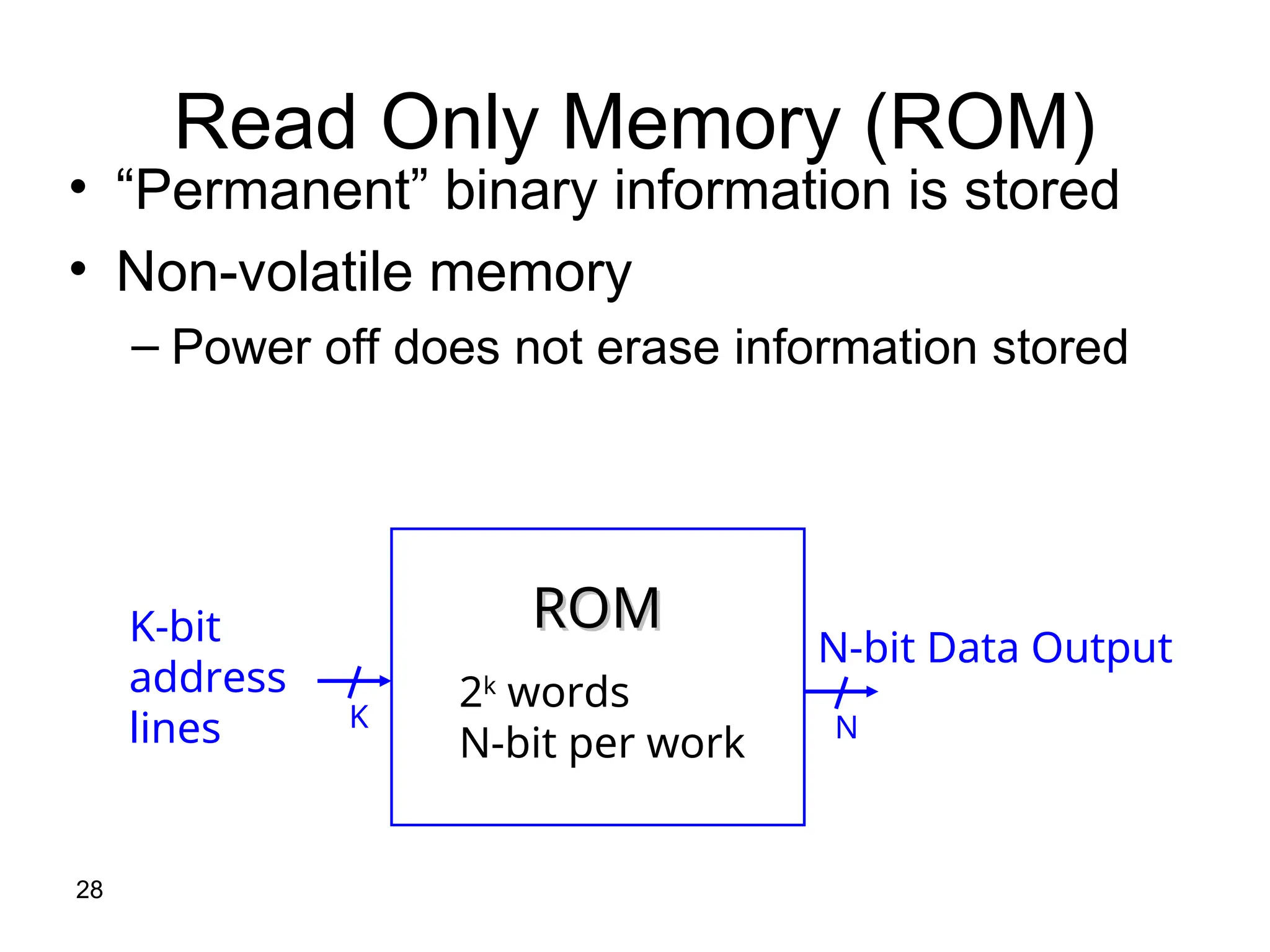
Read Only Memory(ROM)
• “Permanent” binary information is stored
• Non-volatile memory
– Power off does not erase information stored
2k
words
N-bit per work
ROM
ROM
N-bit Data Output
K-bit
address
lines N
K
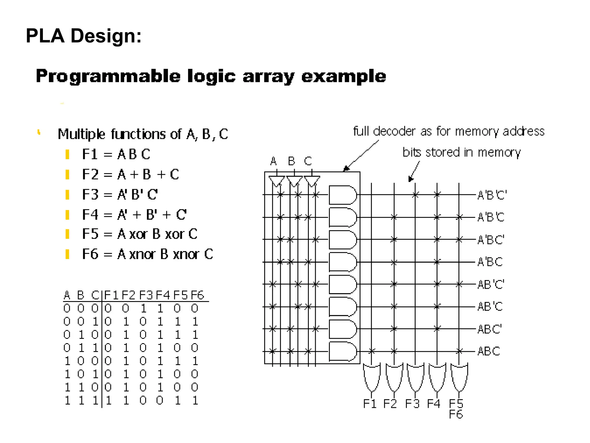
Programmable Logic Array(PLA)
• Compared to a ROM and a PAL, a PLA is the
most flexible having a programmable set of
ANDs combined with a programmable set of
ORs.
• Advantages
– A PLA can have large N and M permitting
implementation of equations that are impractical for a
ROM (because of the number of inputs, N, required
– A PLA has all of its product terms connectable to all
outputs, overcoming the problem of the limited inputs
to the PAL Ors
– Some PLAs have outputs that can be complemented,
adding POS functions
36.
• Disadvantages
– Often,the product term count limits the application of
a PLA.
– Two-level multiple-output optimization is required to
reduce the number of product terms in an
implementation, helping to fit it into a PLA.
– Multi-level circuit capability available in PAL not
available in PLA. PLA requires external connections
to do multi-level circuits.
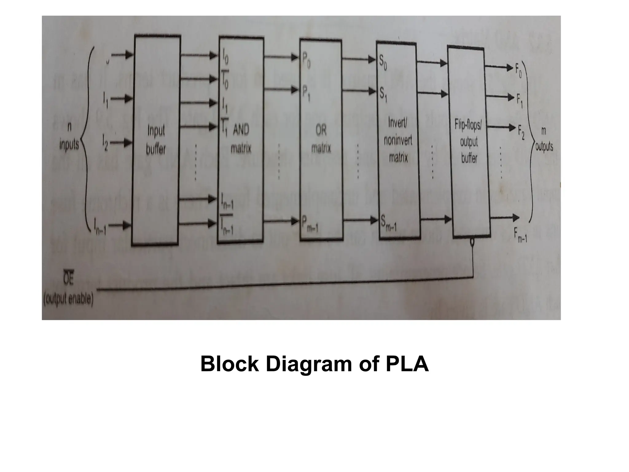
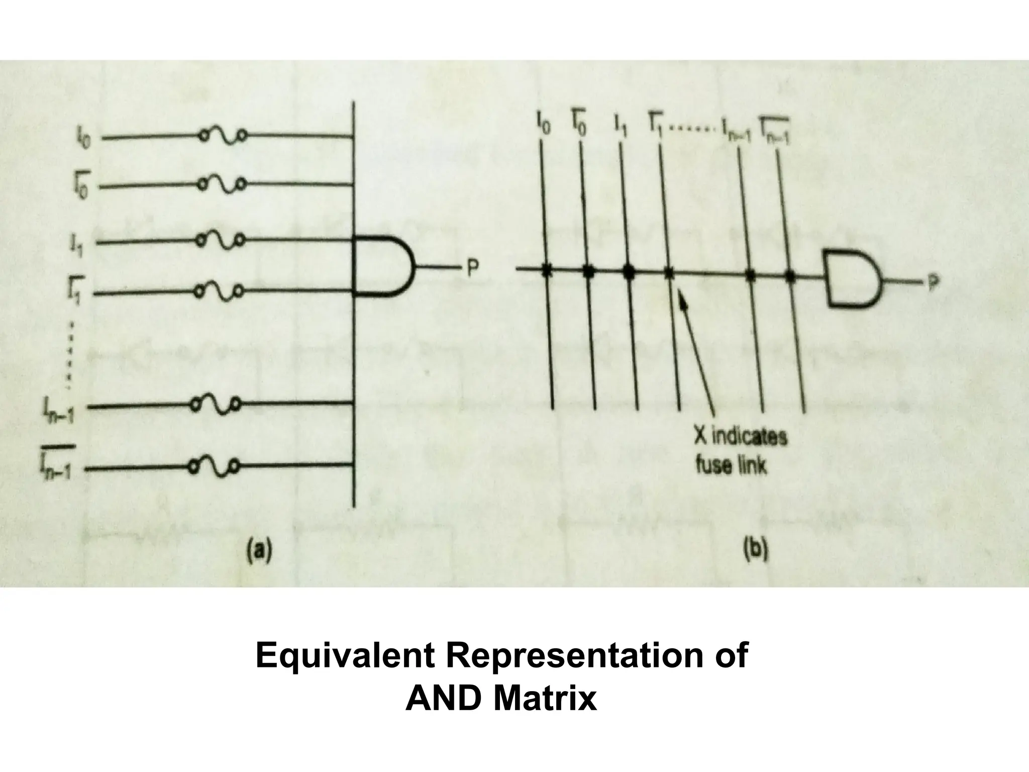
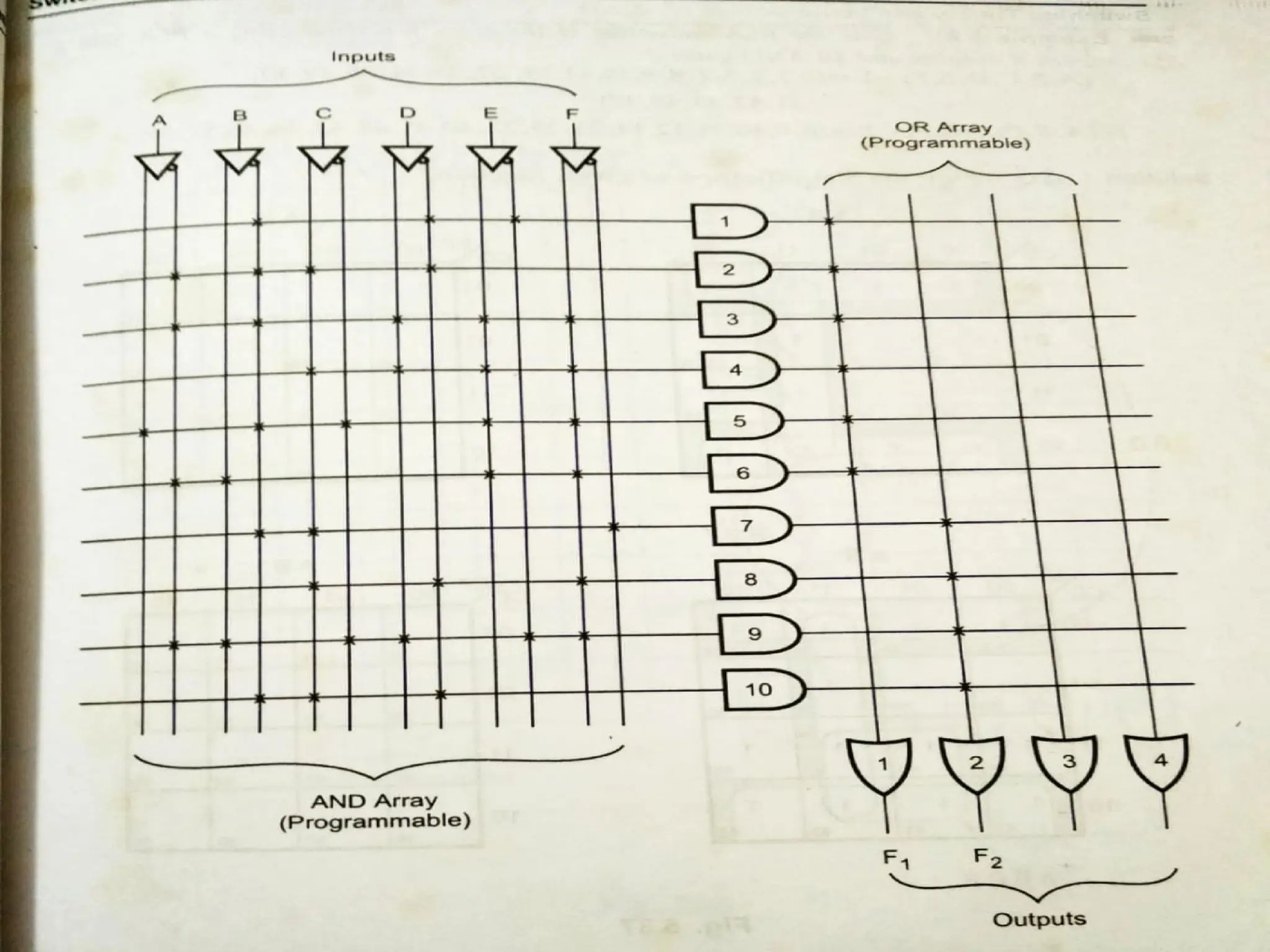
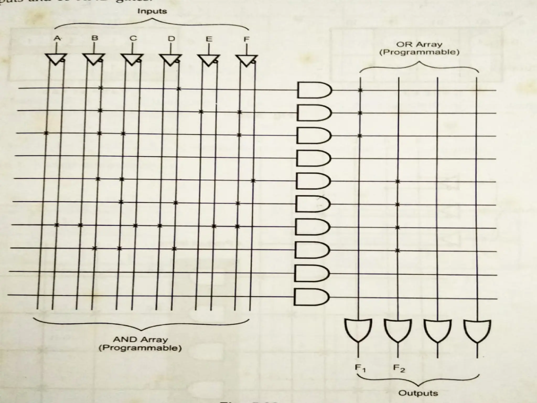
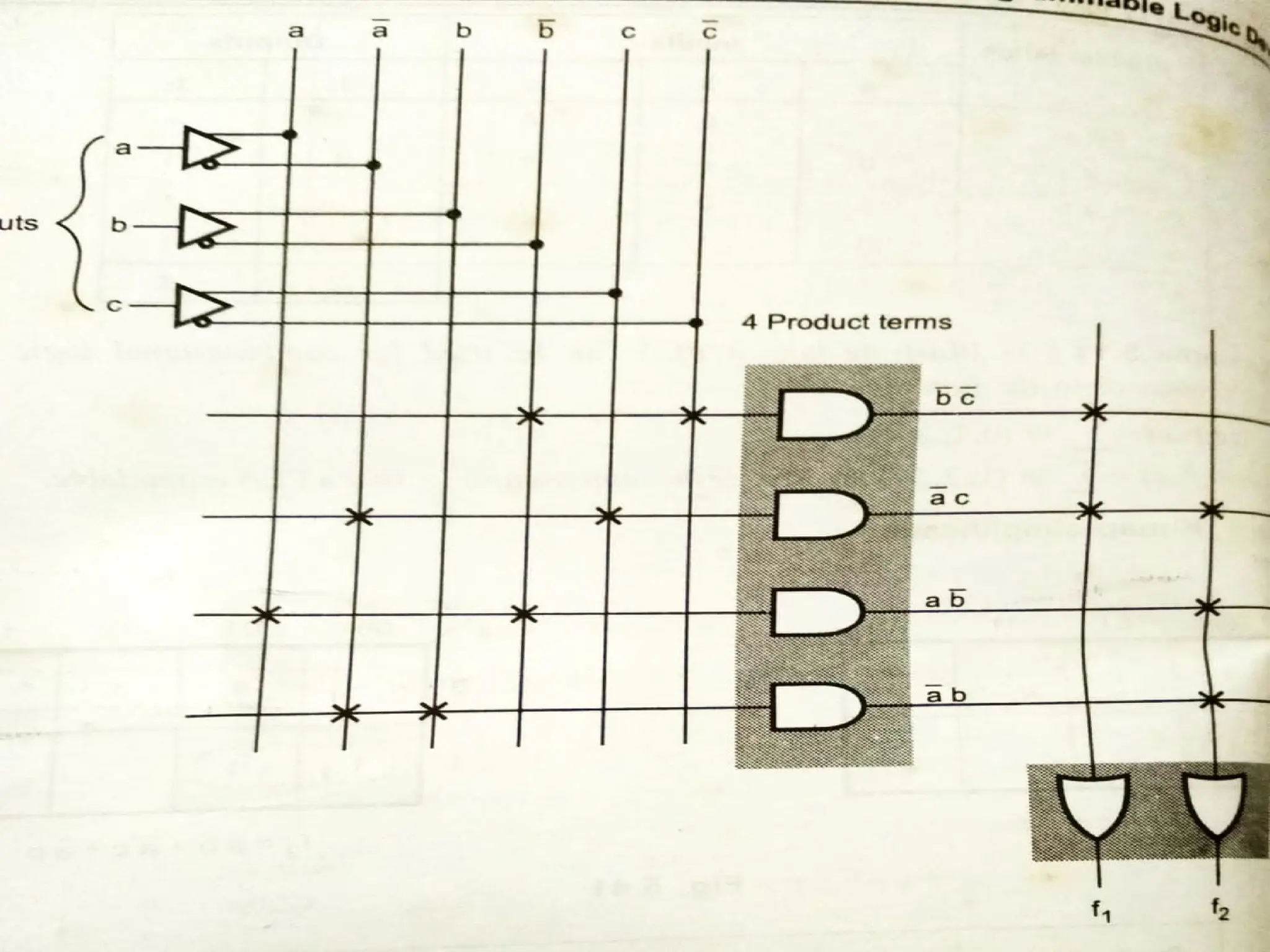
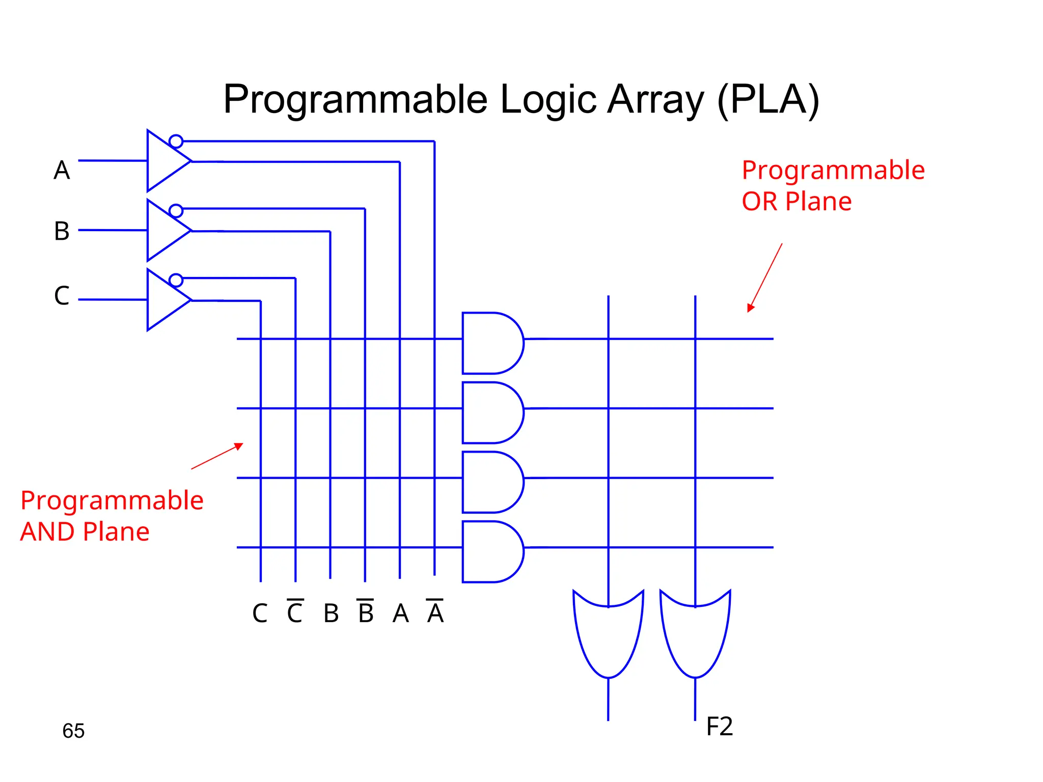
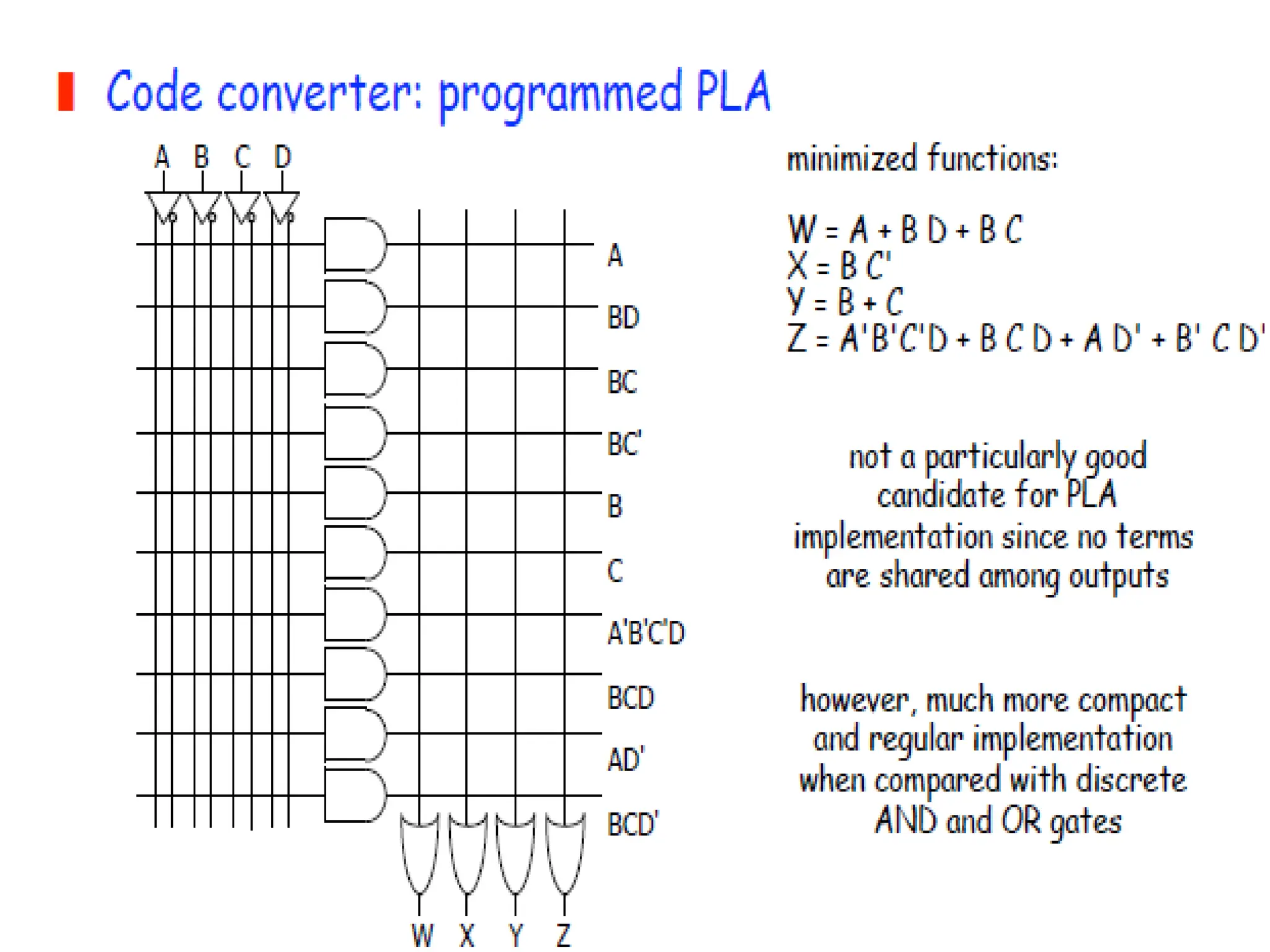
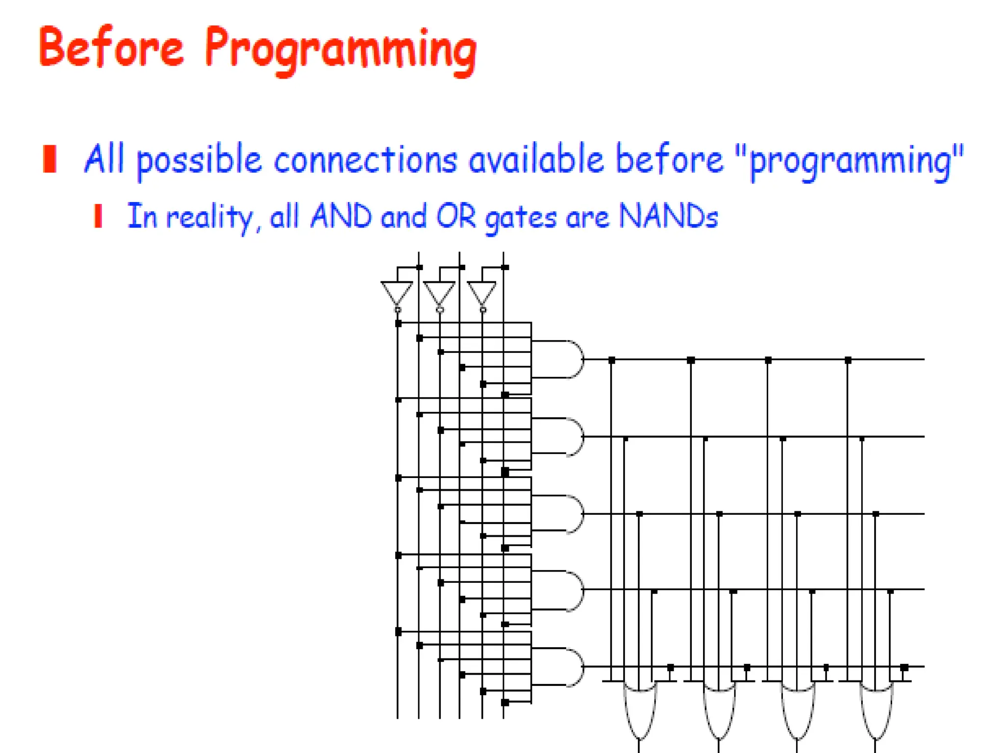
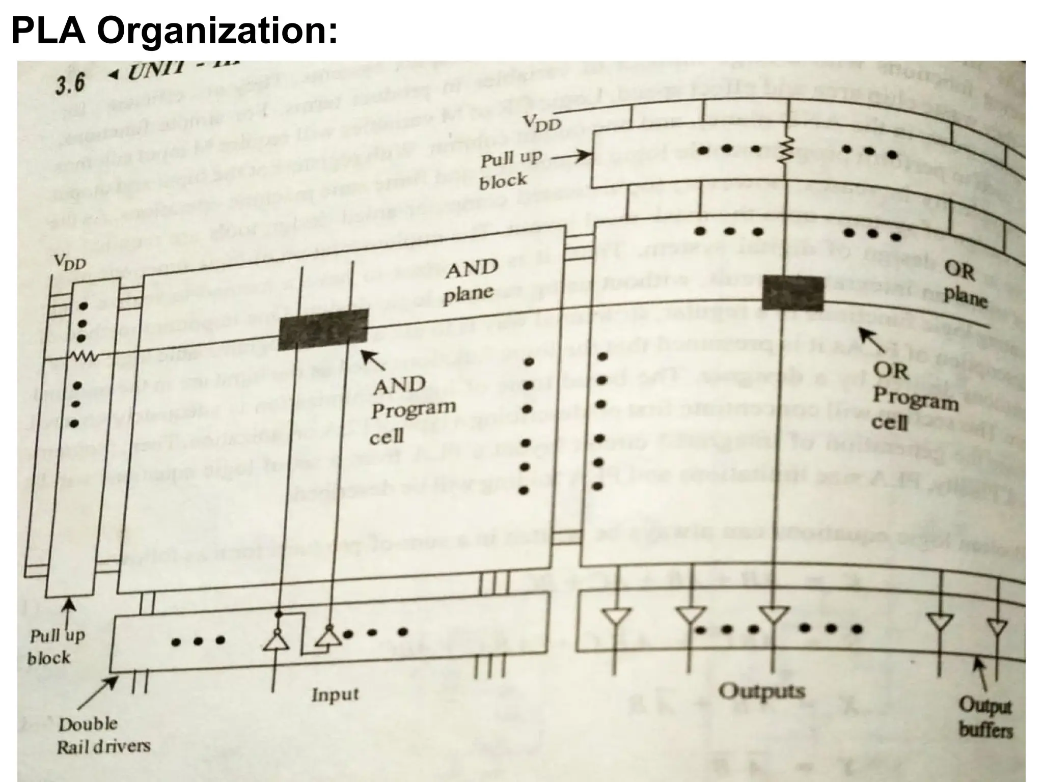
A programmable logicarray (PLA) is a kind of programmable
logic device used to implement combinational logic circuits.
The PLA has a set of programmable AND gate planes, which link
to a set of programmable OR gate planes, which can then be conditionally
complemented to produce an output. It has 2N
AND Gates for N input
variables, and for M outputs from PLA, there should be M OR Gates, each
with programmable inputs from all of the AND gates.
This layout allows for many logic functions to be synthesized in
the sum of products canonical forms.
PLAs differ from Programmable Array Logic devices in that both the AND
and OR gate planes are programmable.
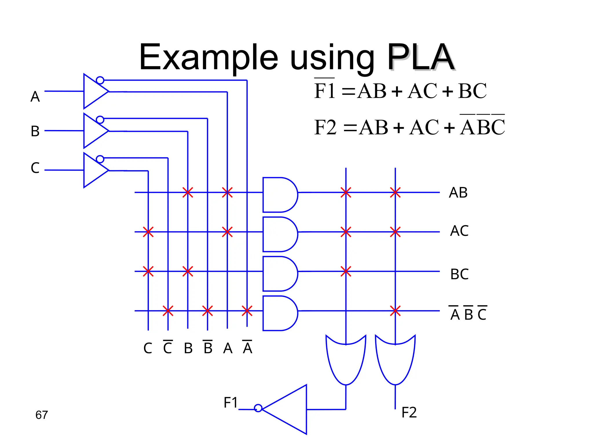
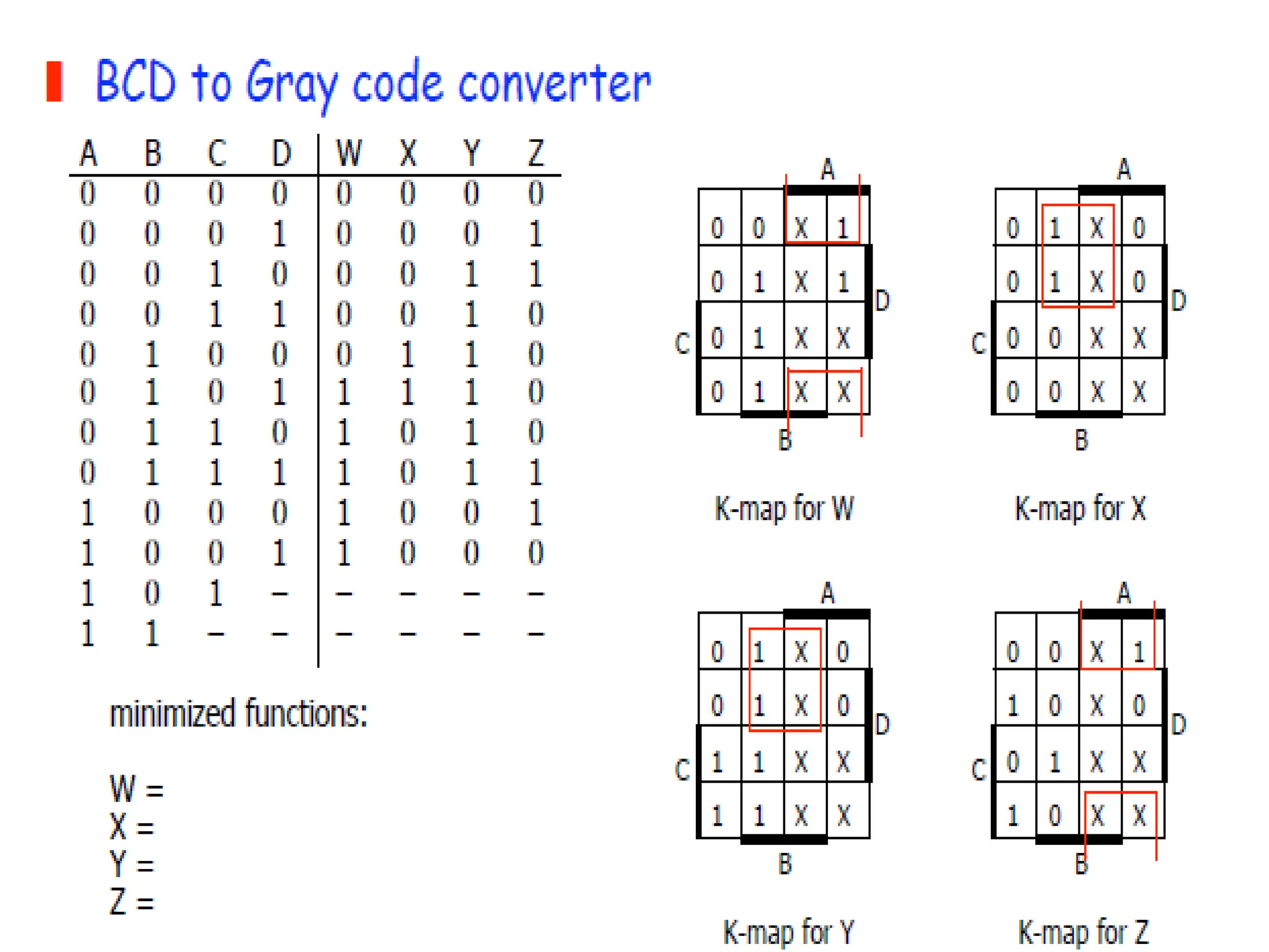
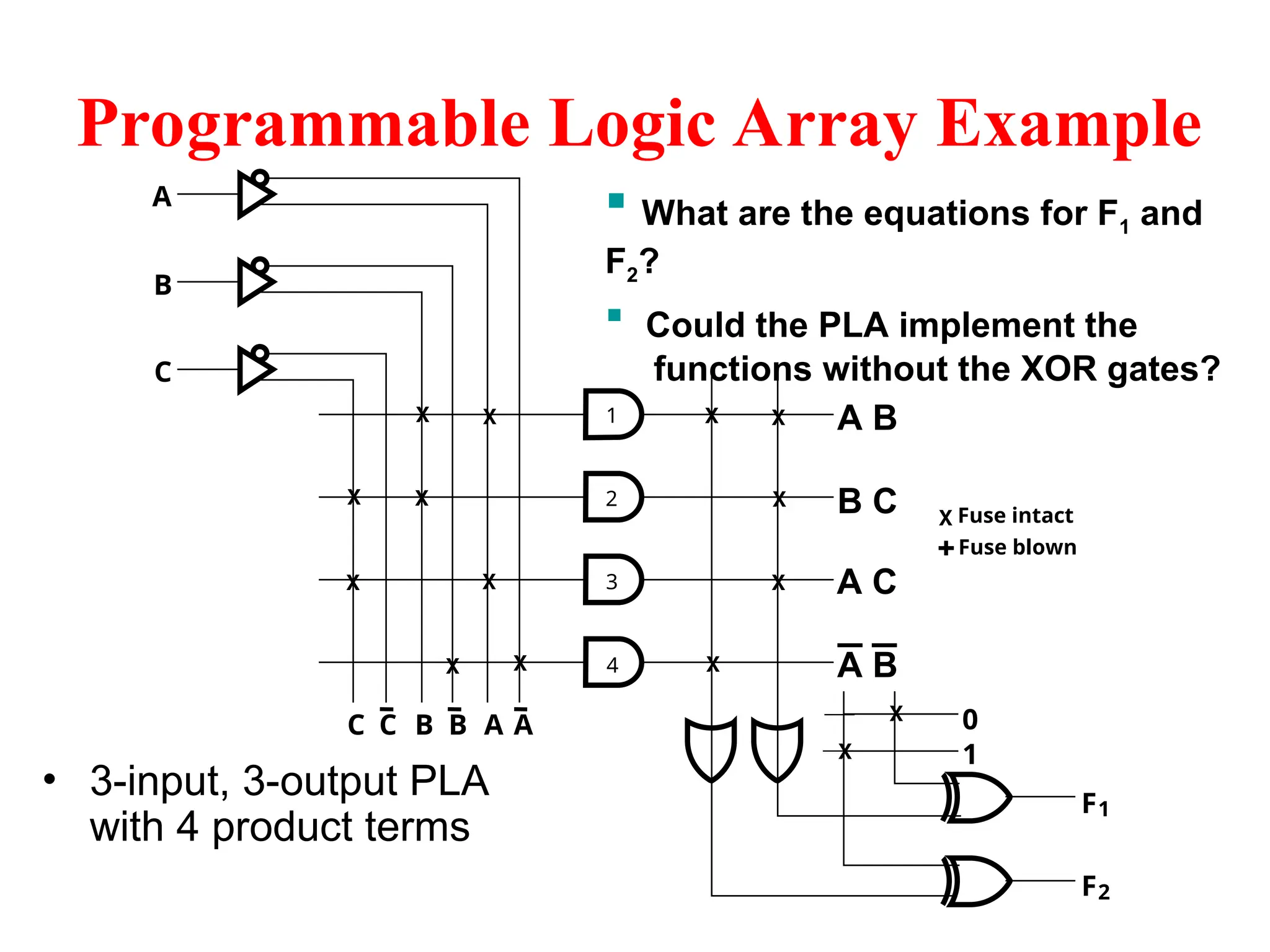
Programmable Logic ArrayExample
Fuse intact
Fuse blown
1
F1
F2
X
A
B
C
C C B B A A 0
1
2
3
4
X
X
X
X X
X
X
X
X
X
X
X
X
X A B
A C
B C
A B
X
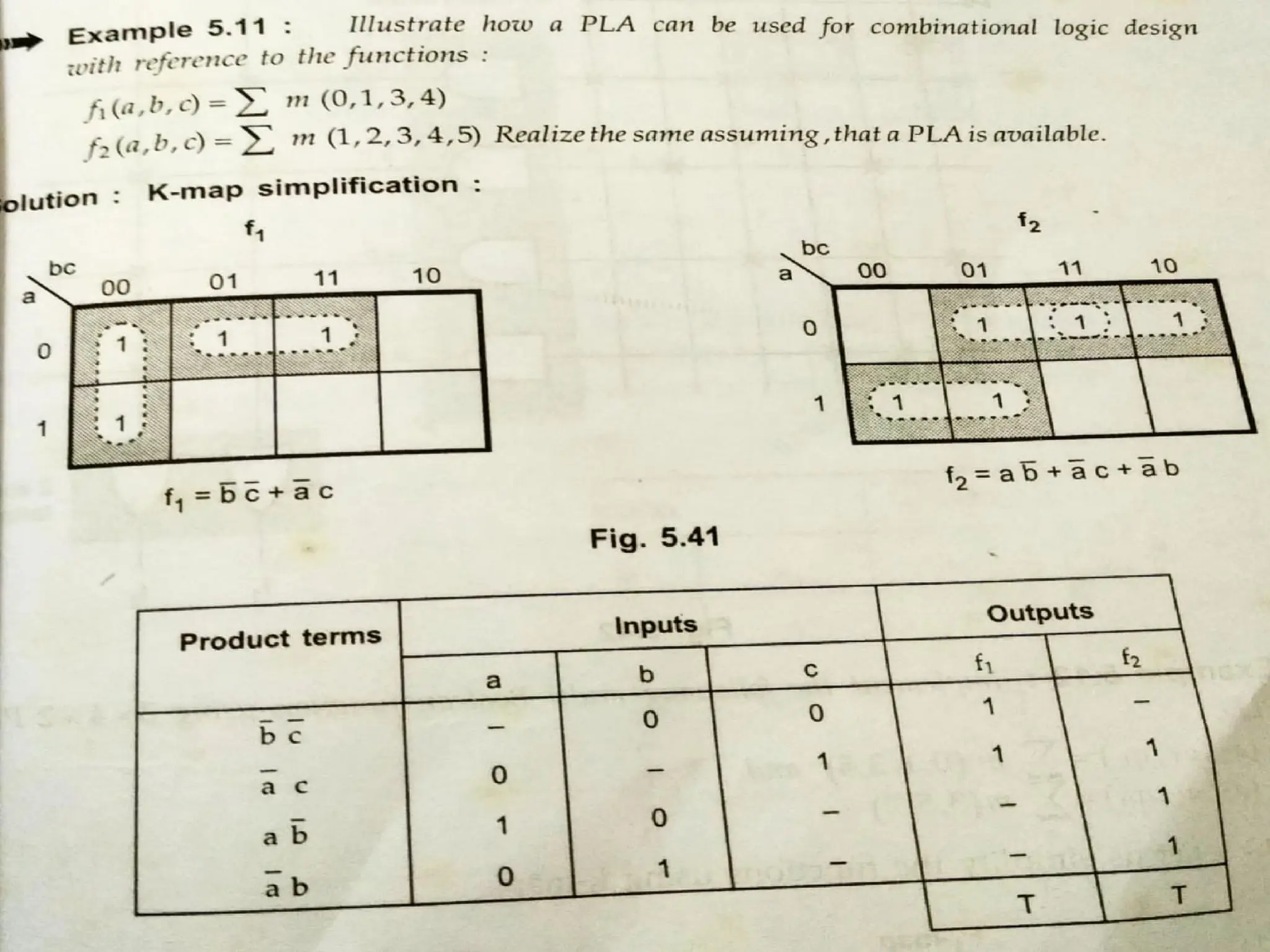
• 3-input, 3-output PLA
with 4 product terms
What are the equations for F1 and
F2?
Could the PLA implement the
functions without the XOR gates?
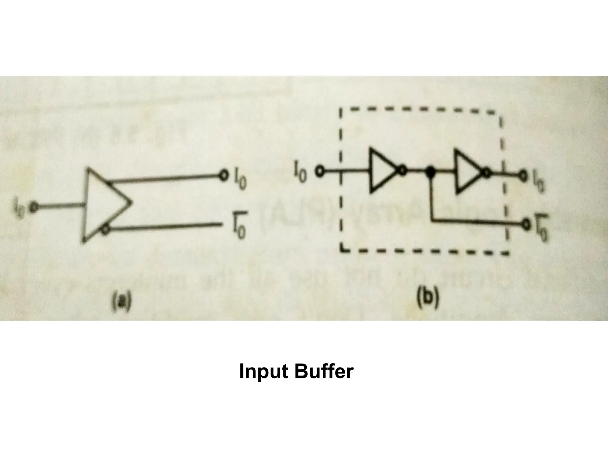
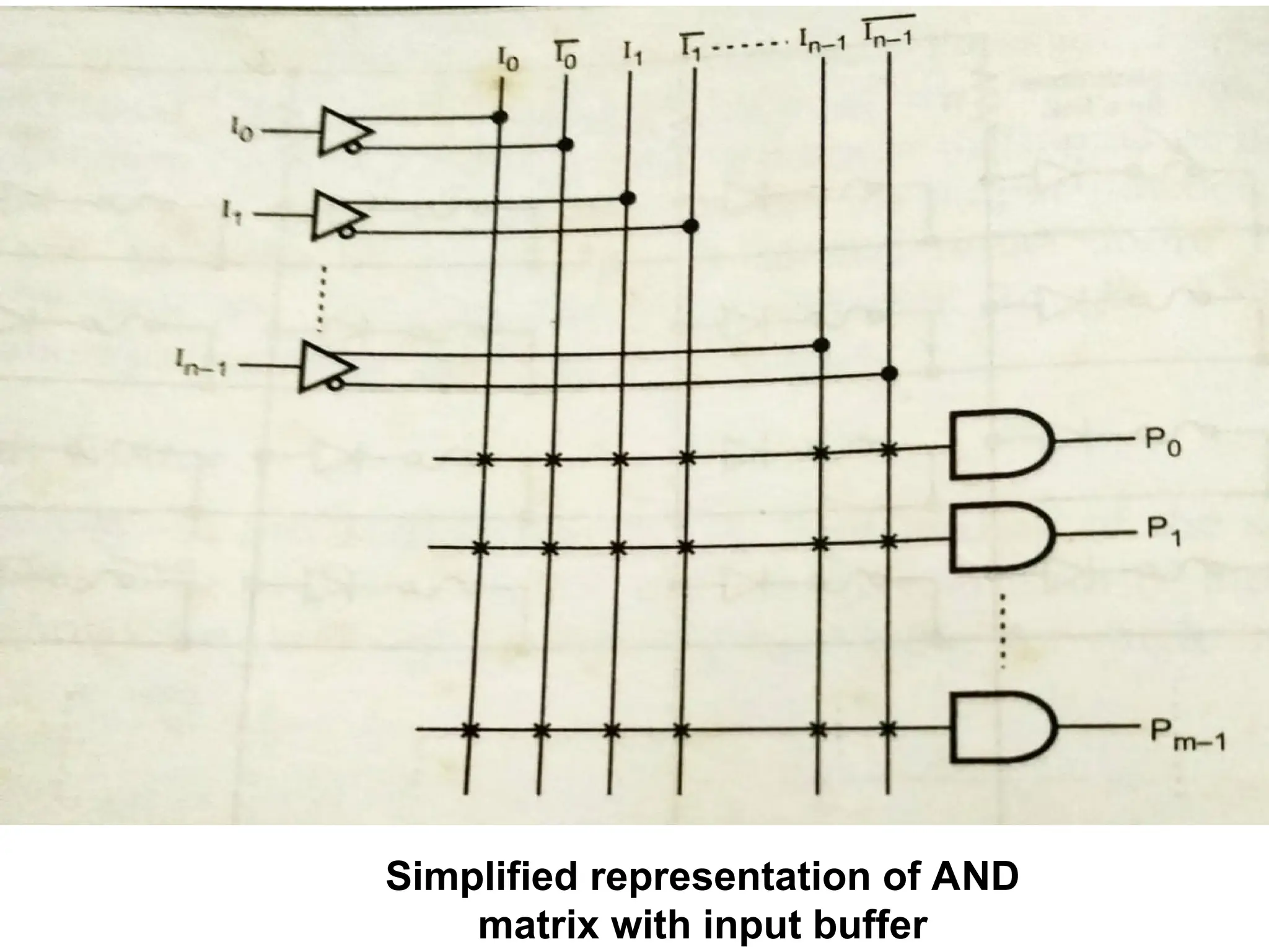
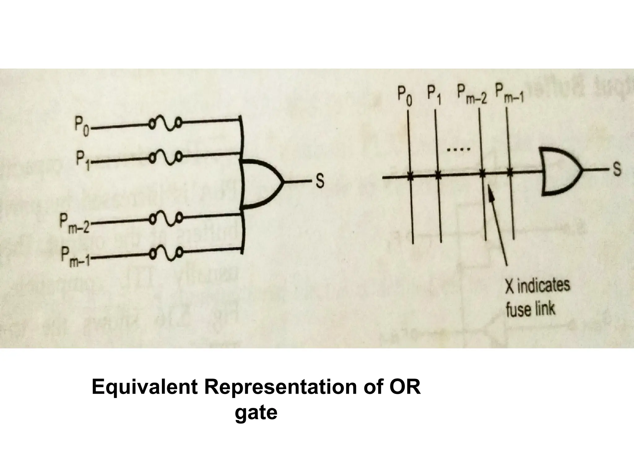
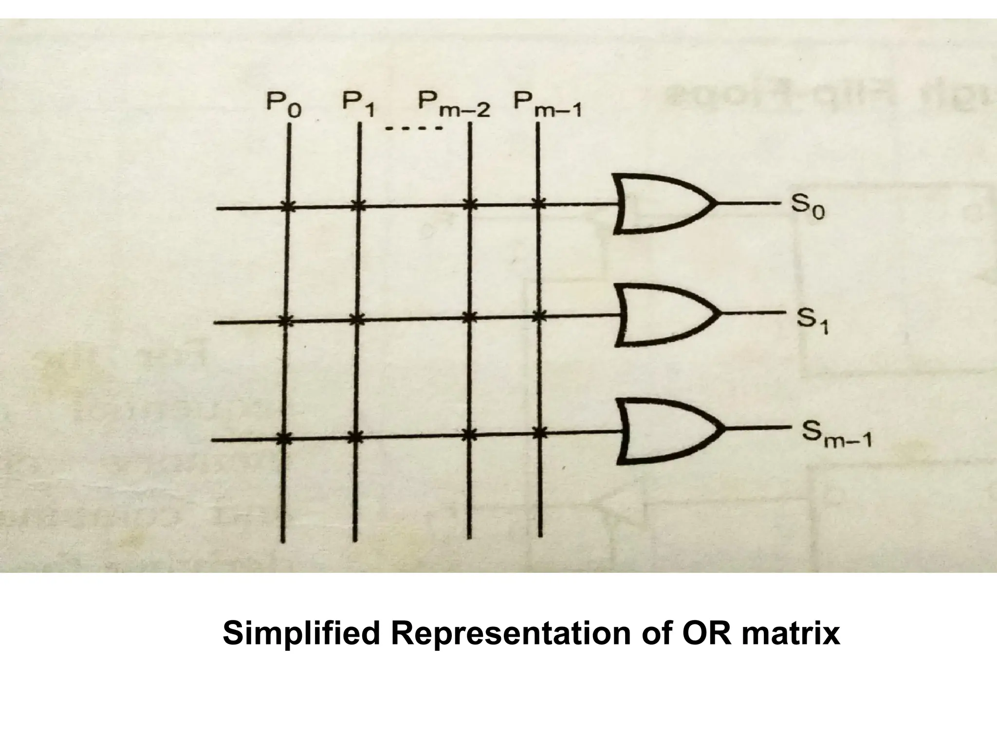
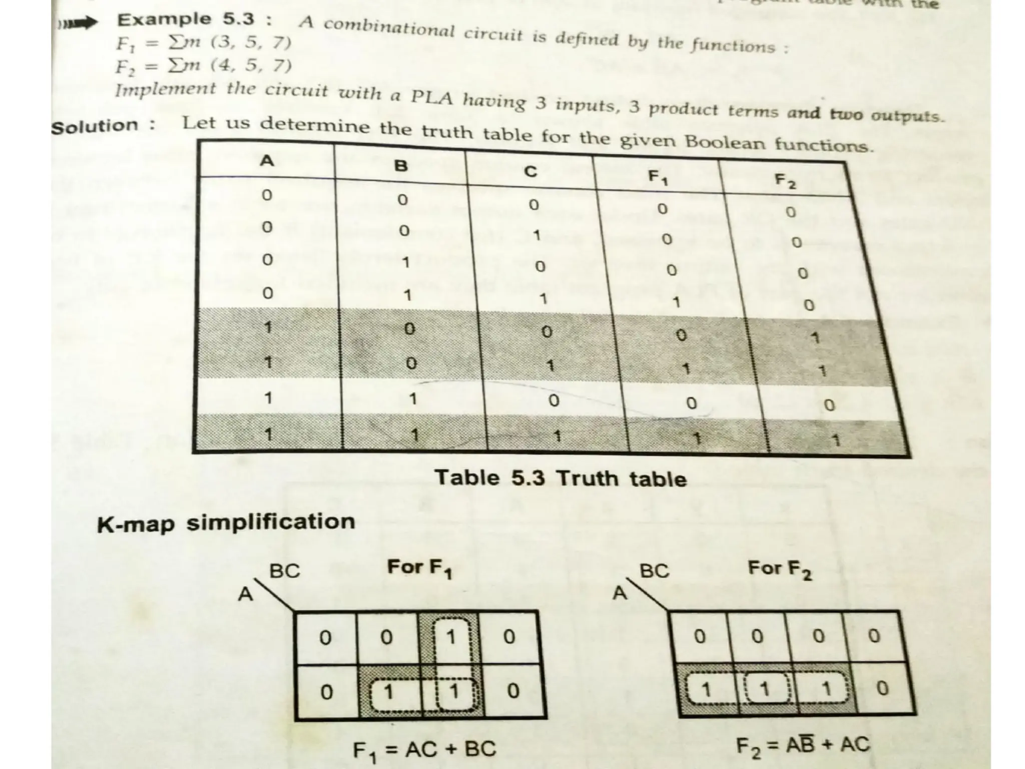
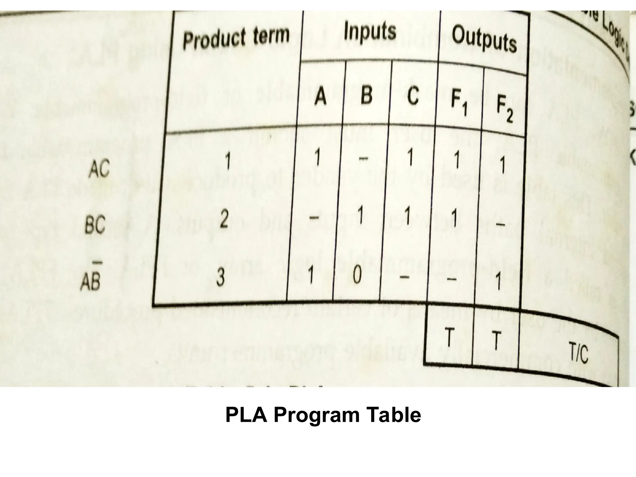
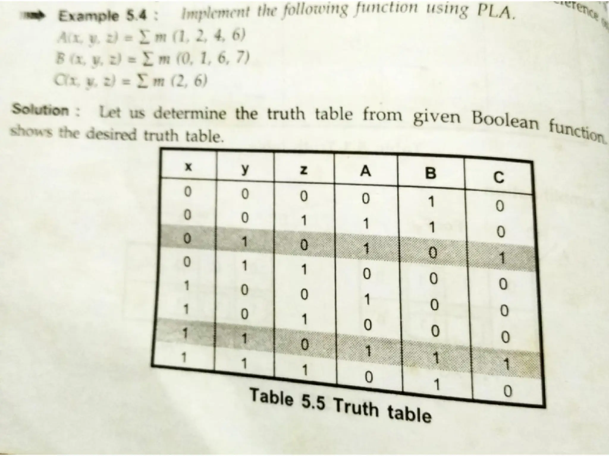
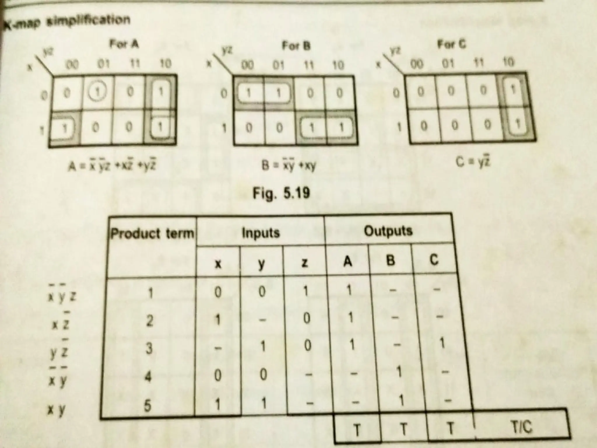
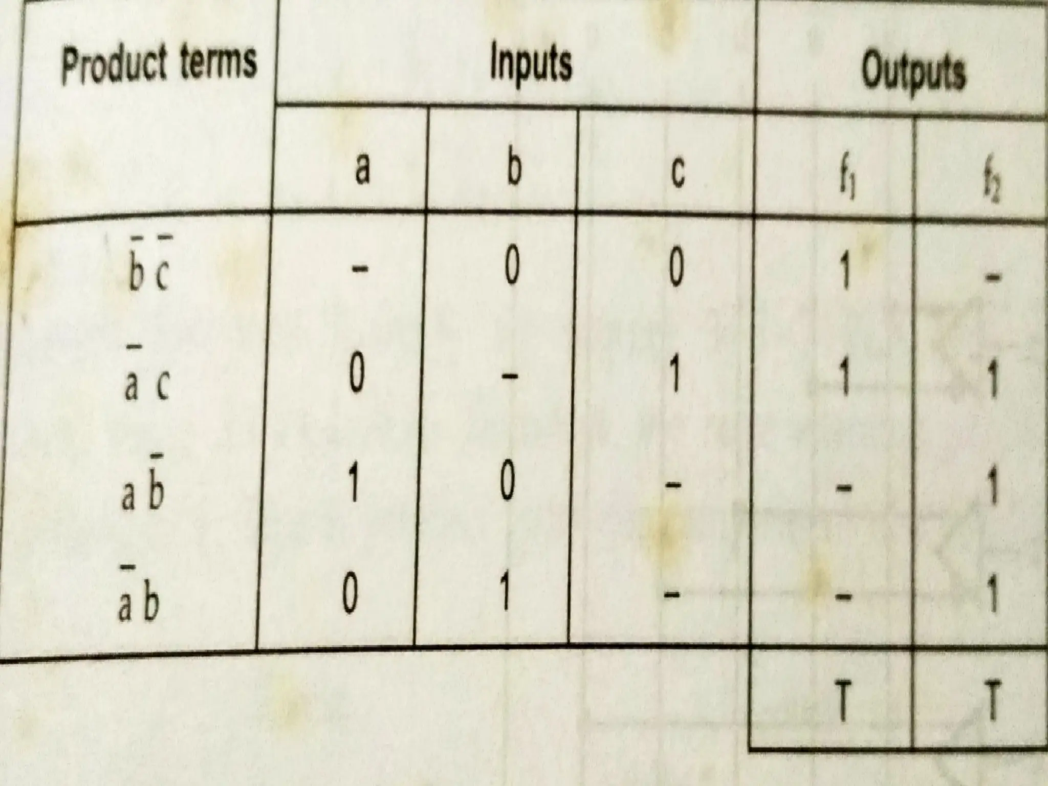
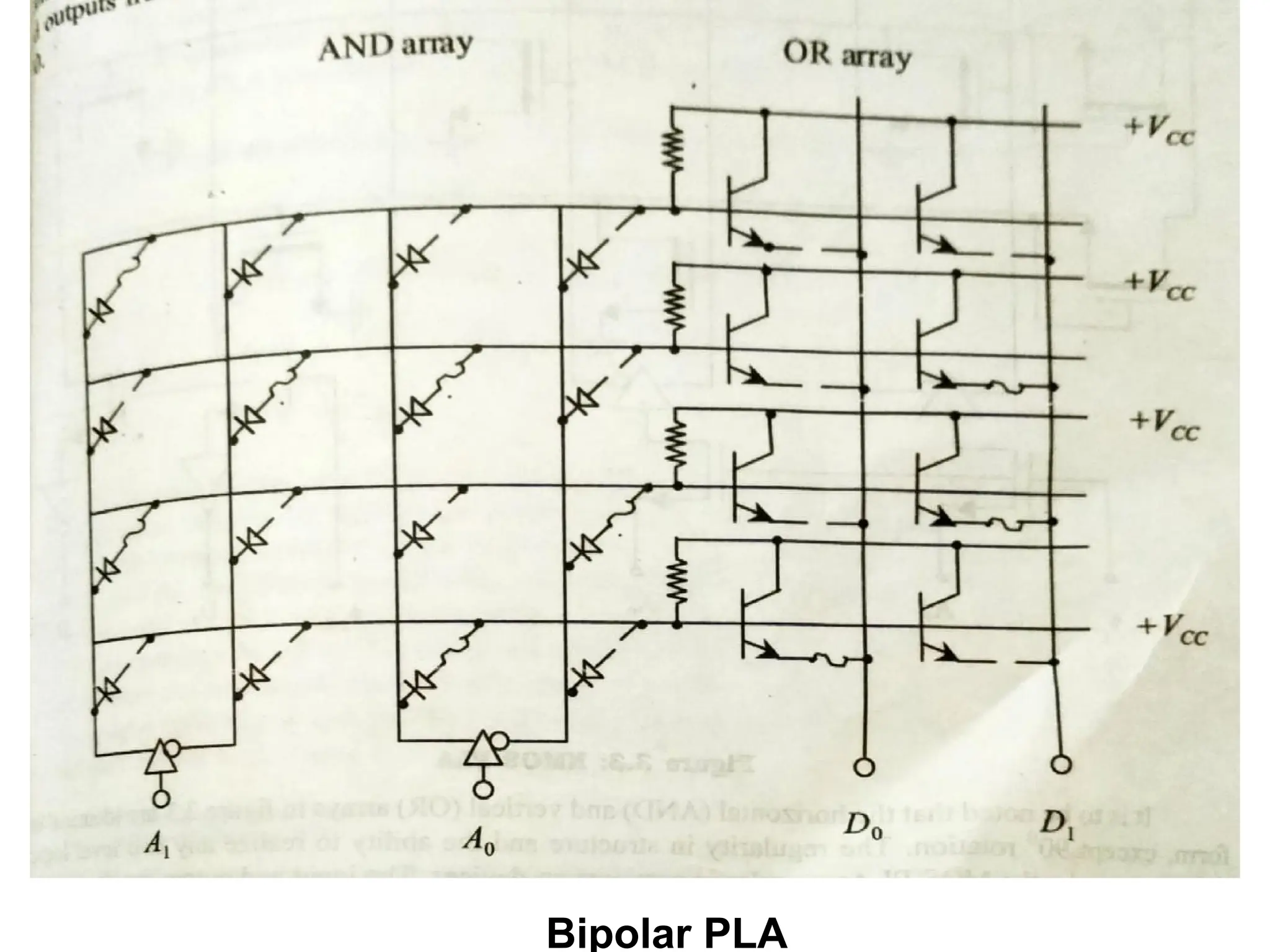
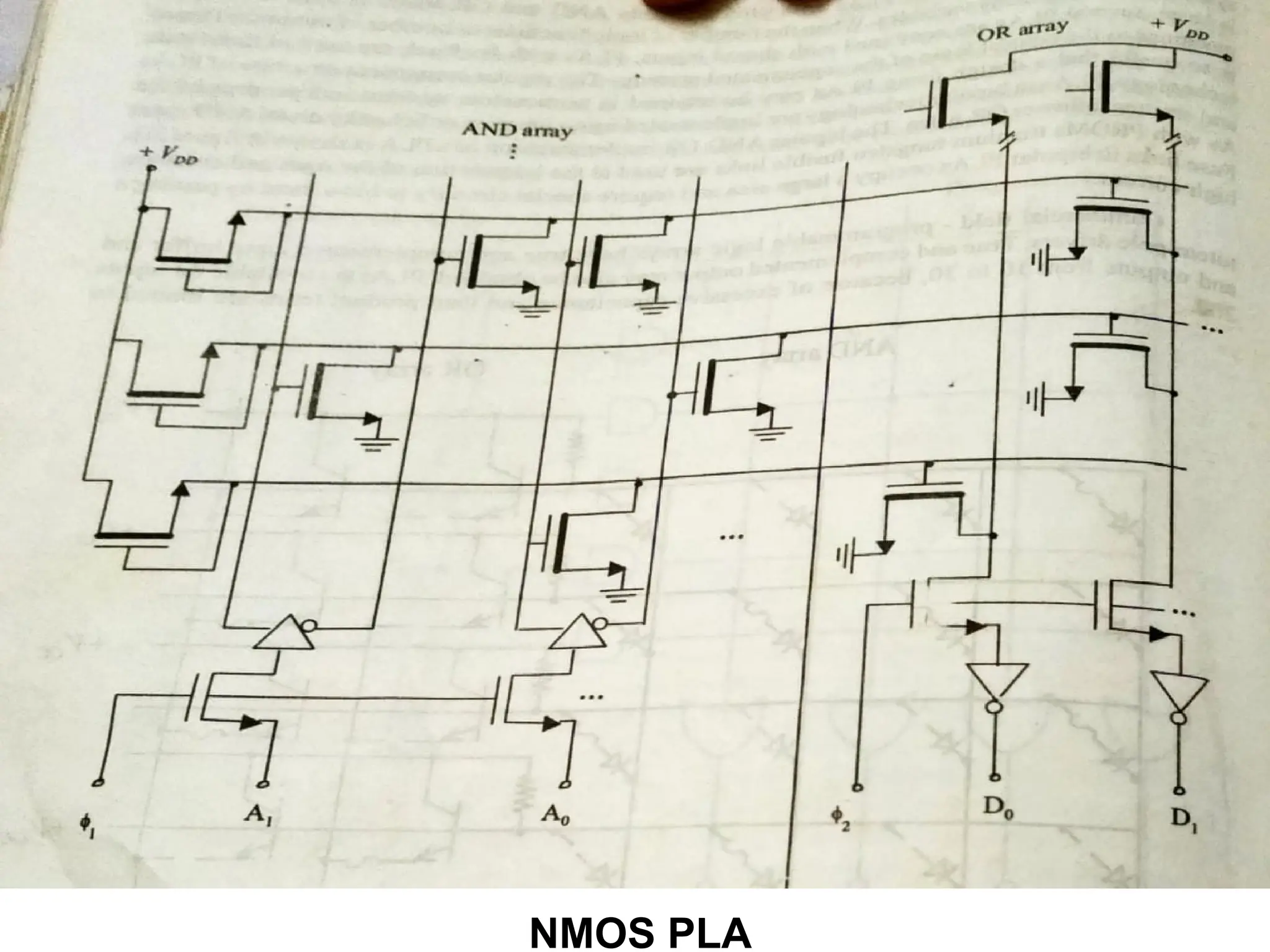
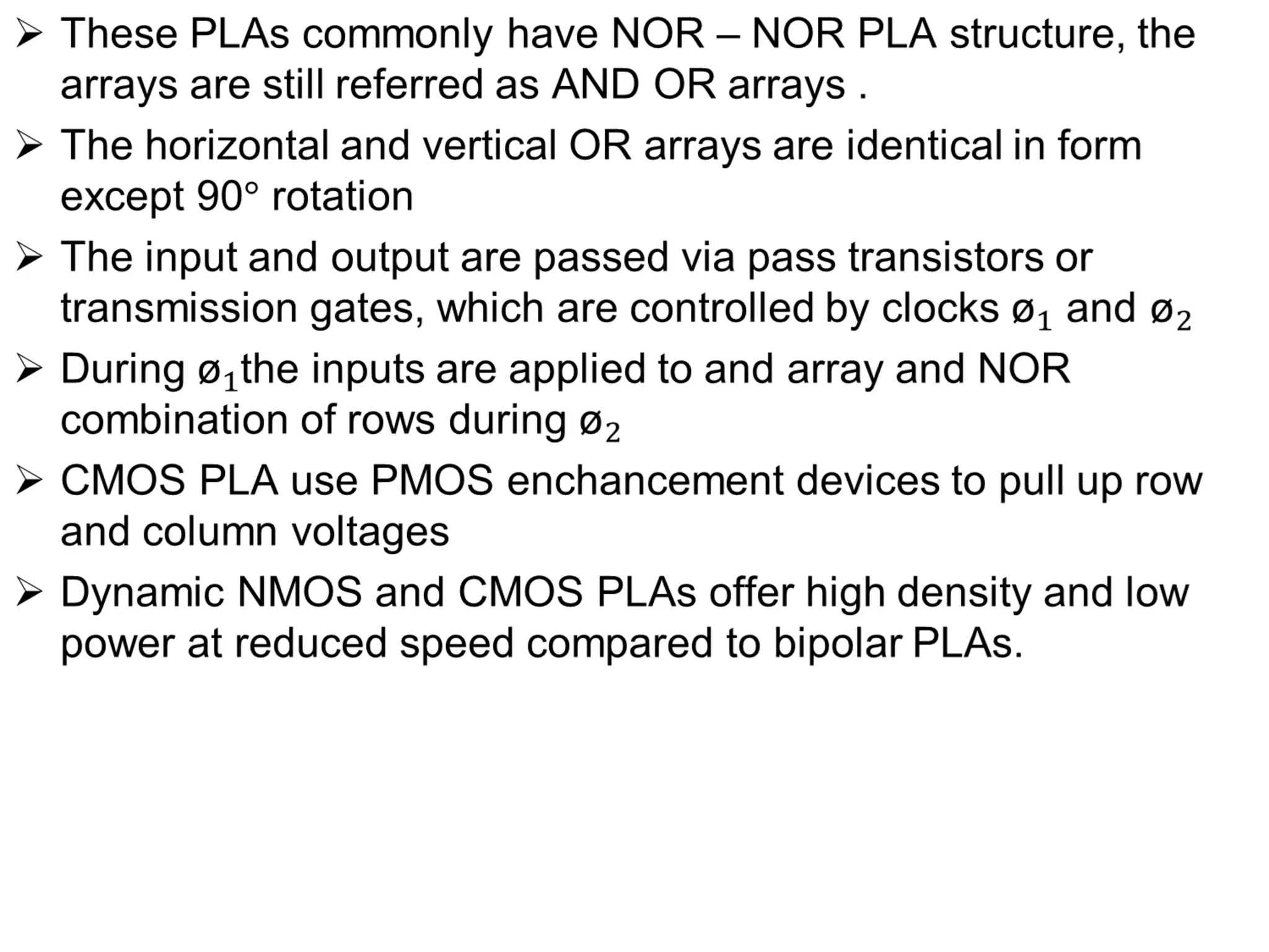
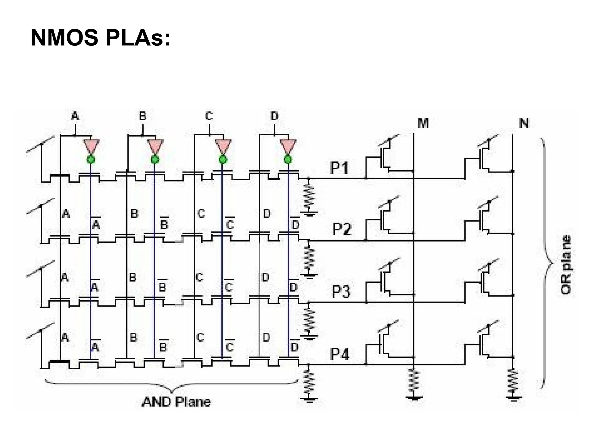
PLA consistsof two major sub sections or planes one is the
And plane, which requires double- rail inputs(each independent
variables and its compliment) to generate the product terms
required by the defining logic equations.
The And plane produces each of the product terms.
The other is the OR plane which forms the dependent results
from these product terms. The OR plane must OR the
necessary product terms to produce the dependent variables.
89.
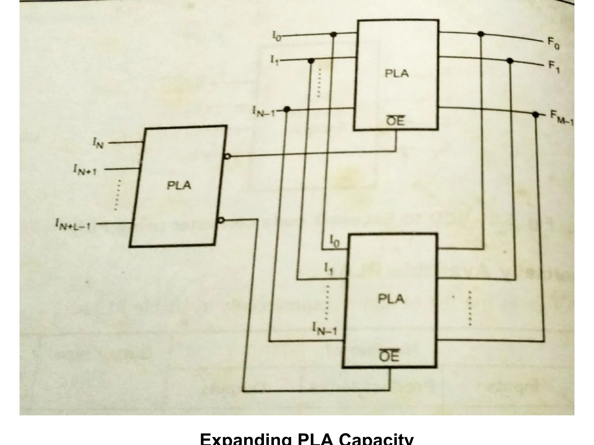
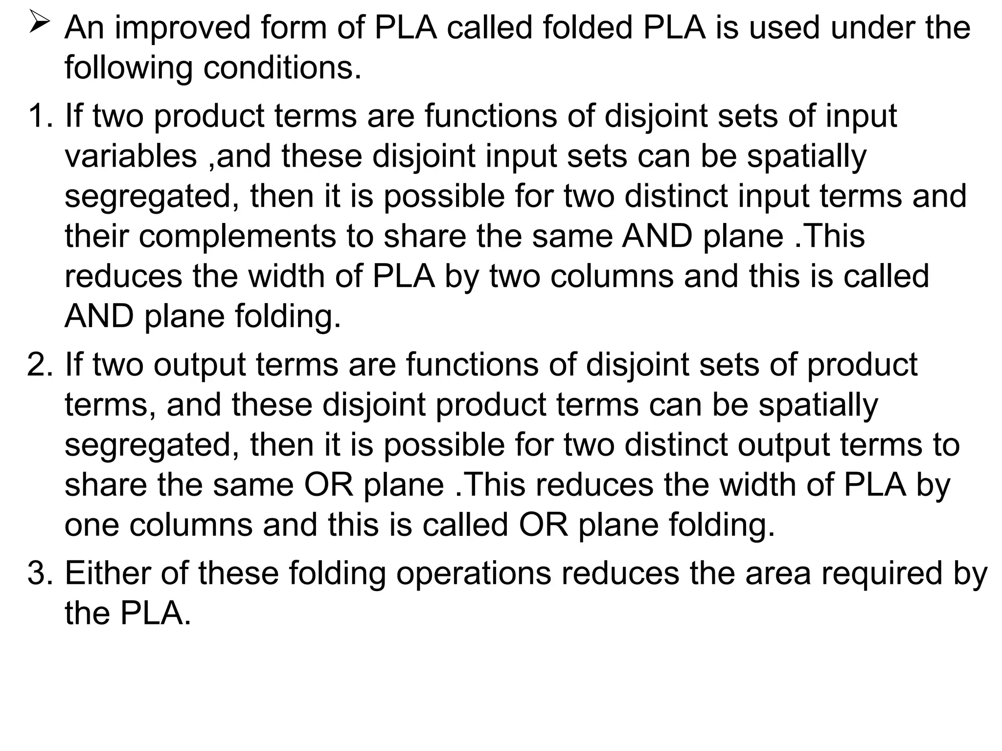
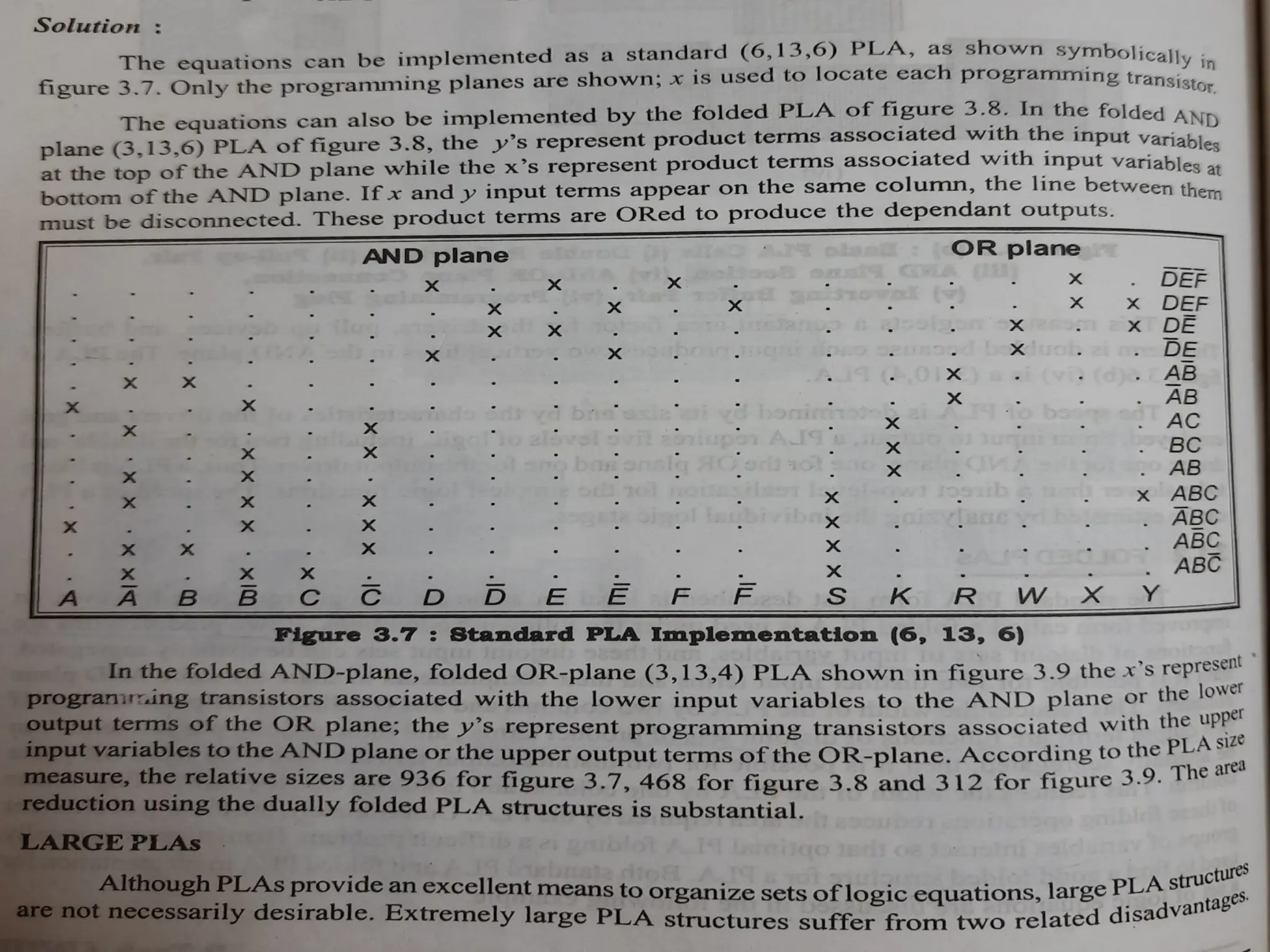
An improvedform of PLA called folded PLA is used under the
following conditions.
1. If two product terms are functions of disjoint sets of input
variables ,and these disjoint input sets can be spatially
segregated, then it is possible for two distinct input terms and
their complements to share the same AND plane .This
reduces the width of PLA by two columns and this is called
AND plane folding.
2. If two output terms are functions of disjoint sets of product
terms, and these disjoint product terms can be spatially
segregated, then it is possible for two distinct output terms to
share the same OR plane .This reduces the width of PLA by
one columns and this is called OR plane folding.
3. Either of these folding operations reduces the area required by
the PLA.
93.
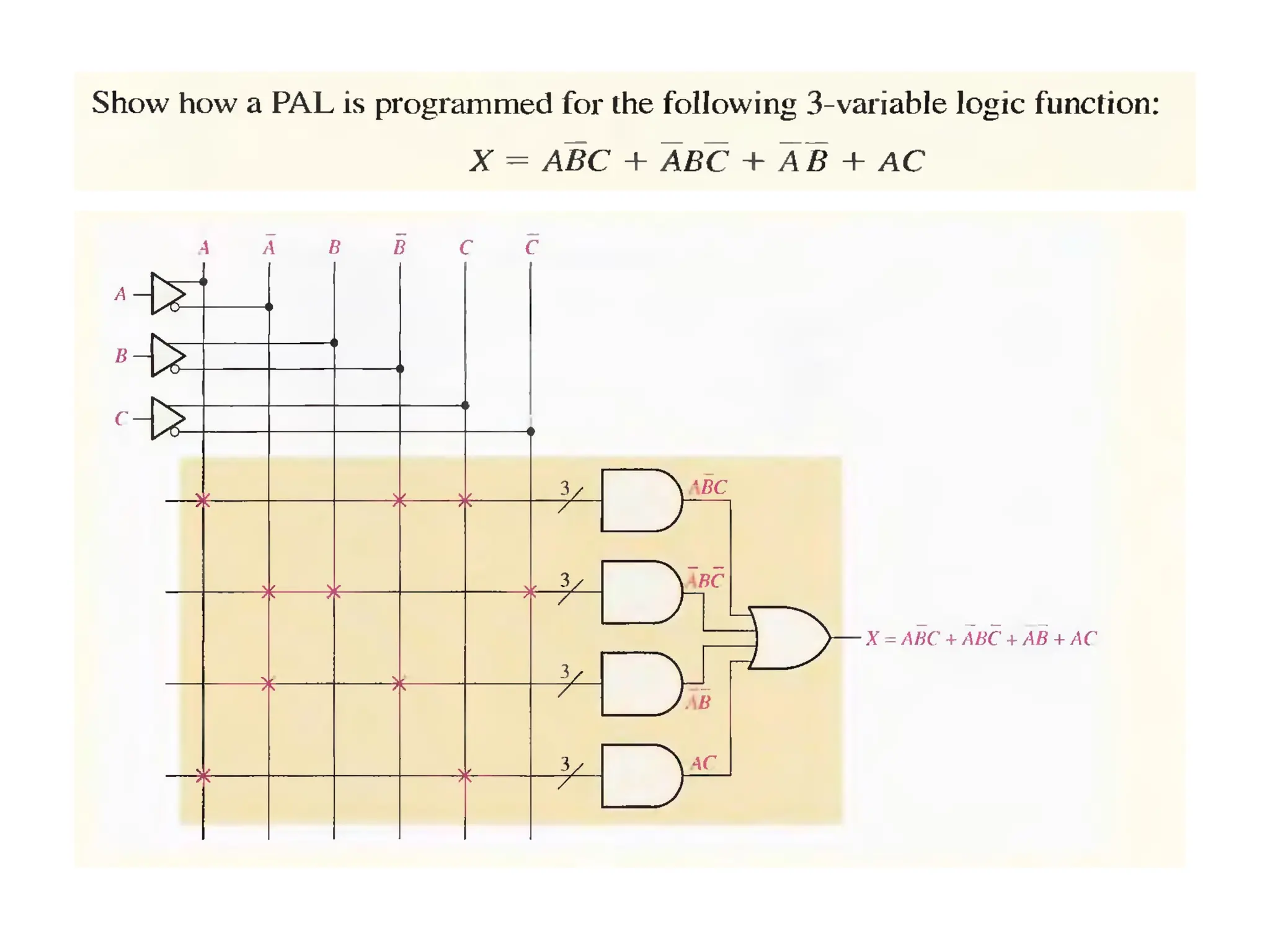
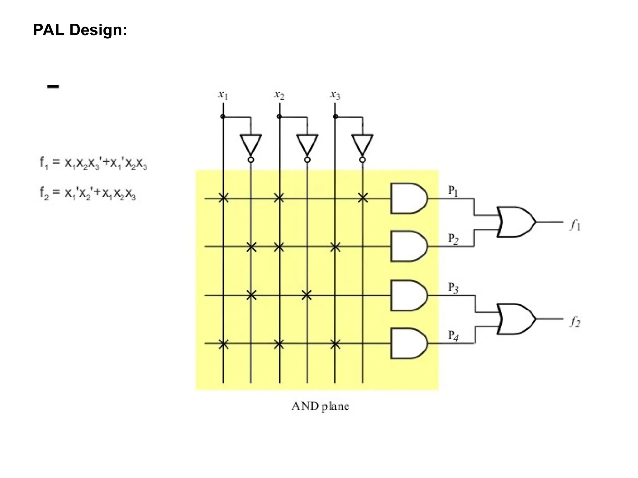
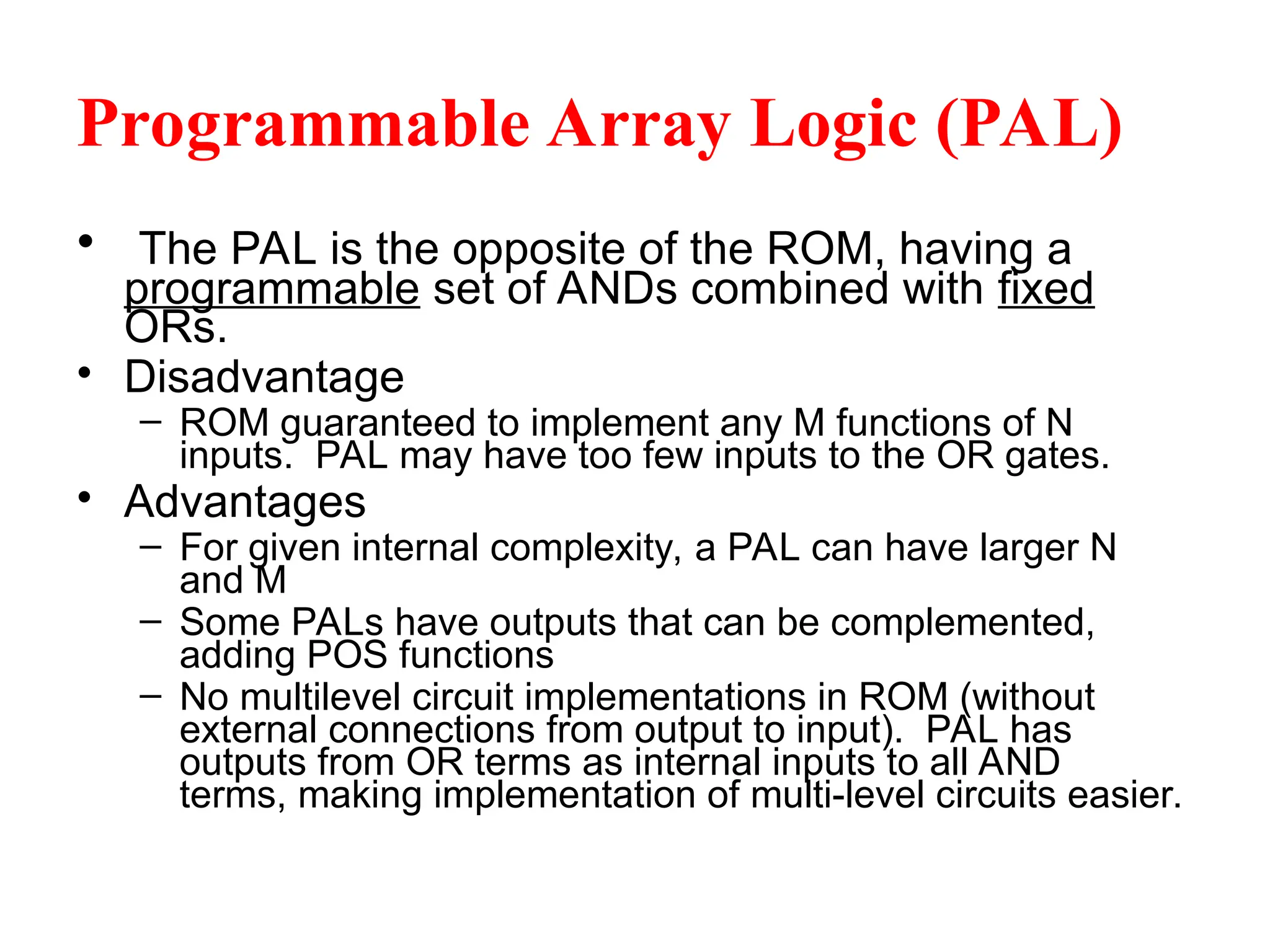
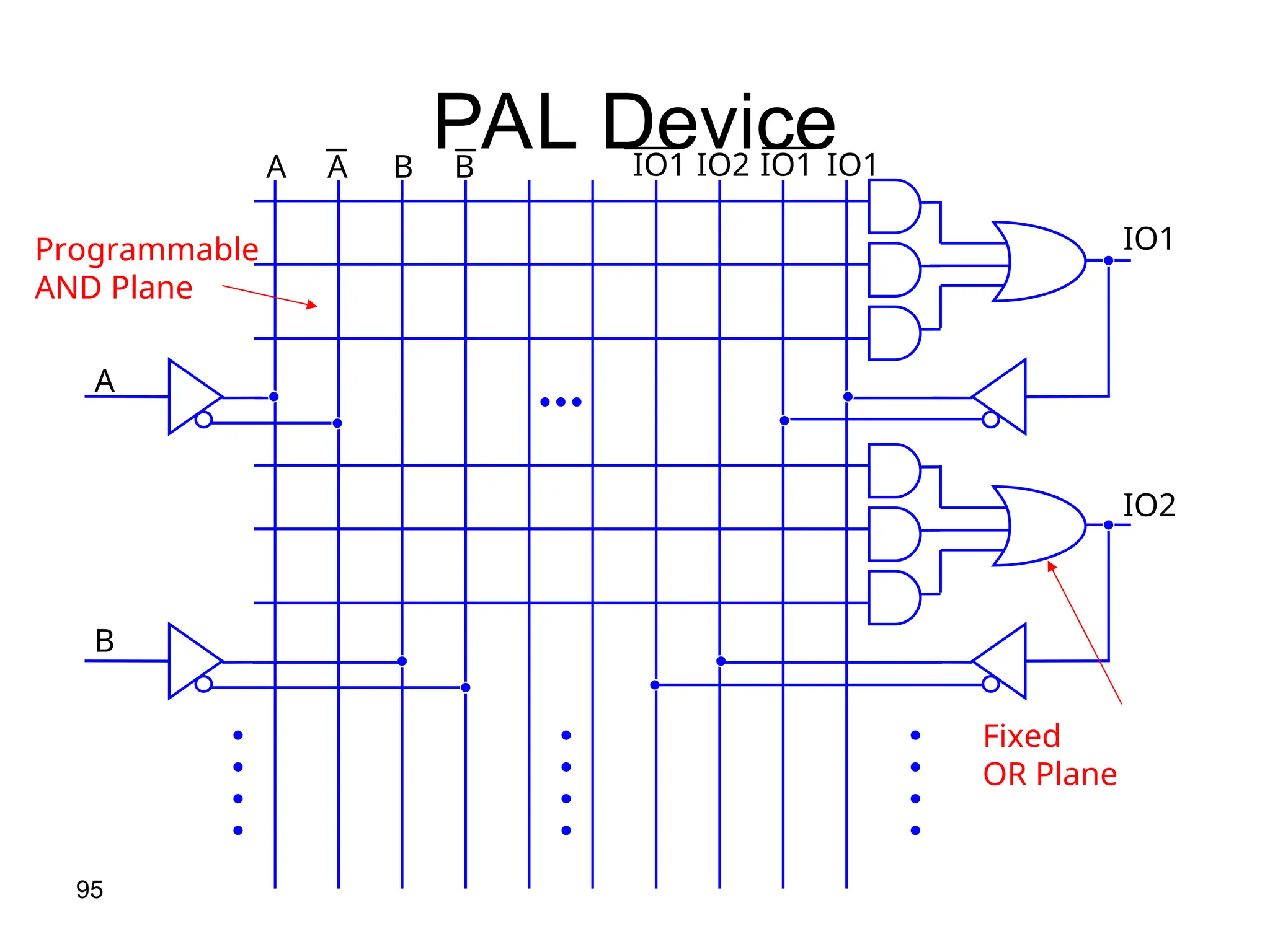
Programmable Array Logic(PAL)
• The PAL is the opposite of the ROM, having a
programmable set of ANDs combined with fixed
ORs.
• Disadvantage
– ROM guaranteed to implement any M functions of N
inputs. PAL may have too few inputs to the OR gates.
• Advantages
– For given internal complexity, a PAL can have larger N
and M
– Some PALs have outputs that can be complemented,
adding POS functions
– No multilevel circuit implementations in ROM (without
external connections from output to input). PAL has
outputs from OR terms as internal inputs to all AND
terms, making implementation of multi-level circuits easier.
94.
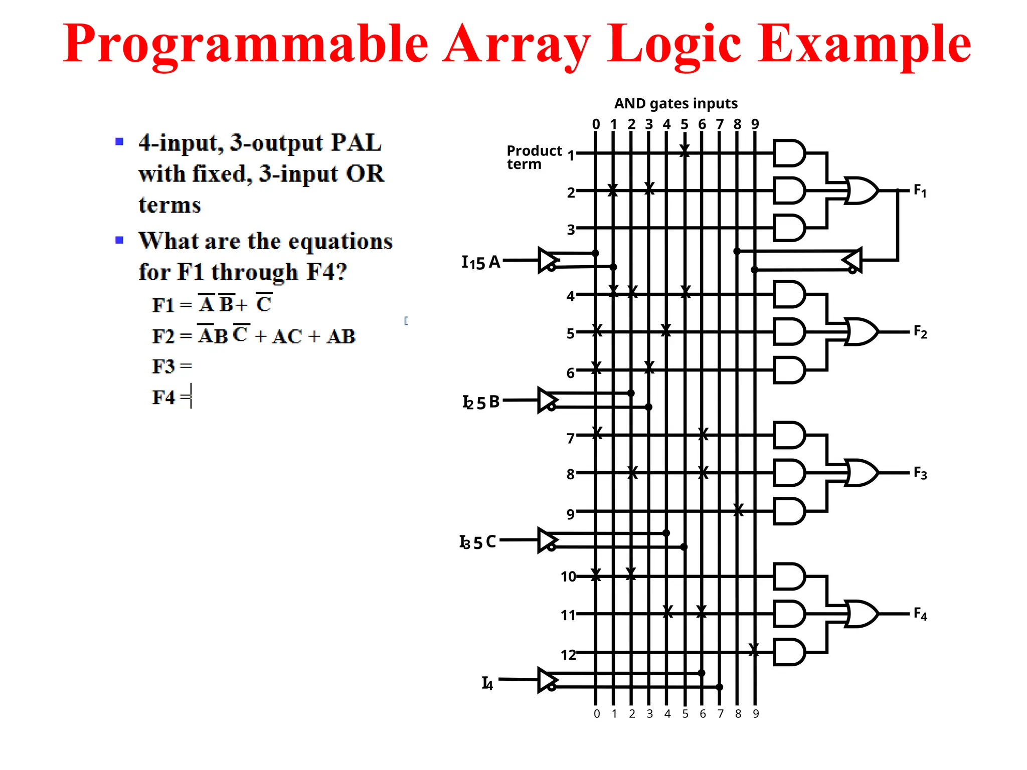
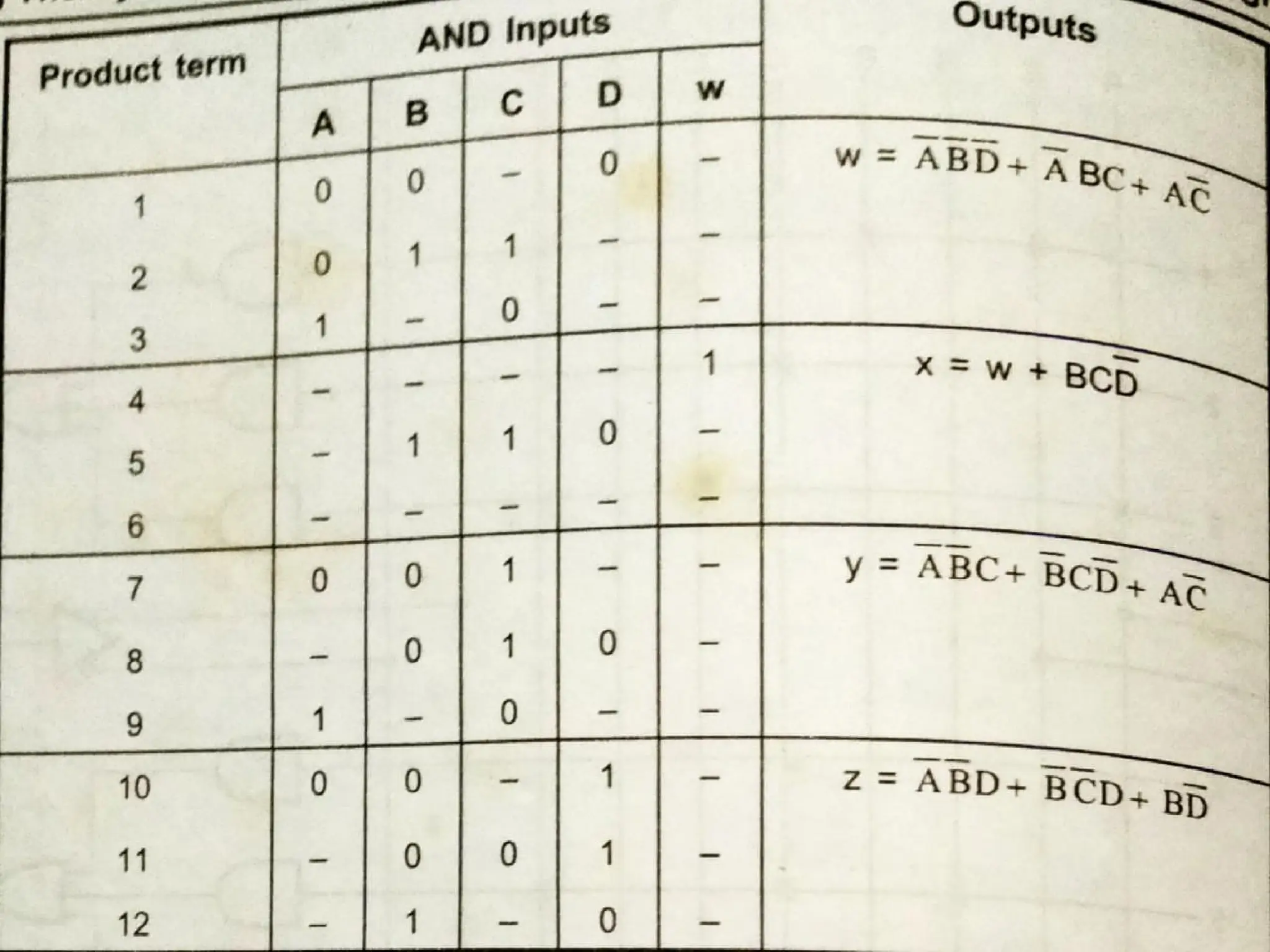
Programmable Array LogicExample
0 9
1 2 3 4 5 6 7 8
AND gates inputs
0 9
Product
term
1
2
3
4
5
6
7
8
9
10
11
12
F1
F2
F3
F4
I3 5C
I2 5B
I15 A
1 2 3 4 5 6 7 8
I4
X X
X X
X X X
X X
X
X
X
X
X
X
X X
X
X X
96
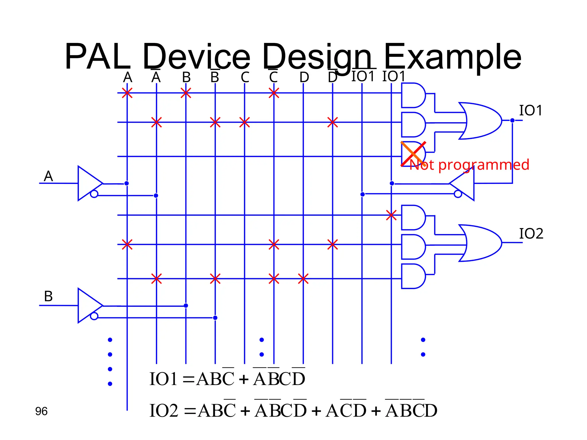
PAL Device DesignExample
A
B
IO1
IO2
IO1 IO1
B B
A A
D
C
B
A
D
C
A
D
C
B
A
C
AB
IO2
D
C
B
A
C
AB
IO1
D D
C C
Not programmed
99.
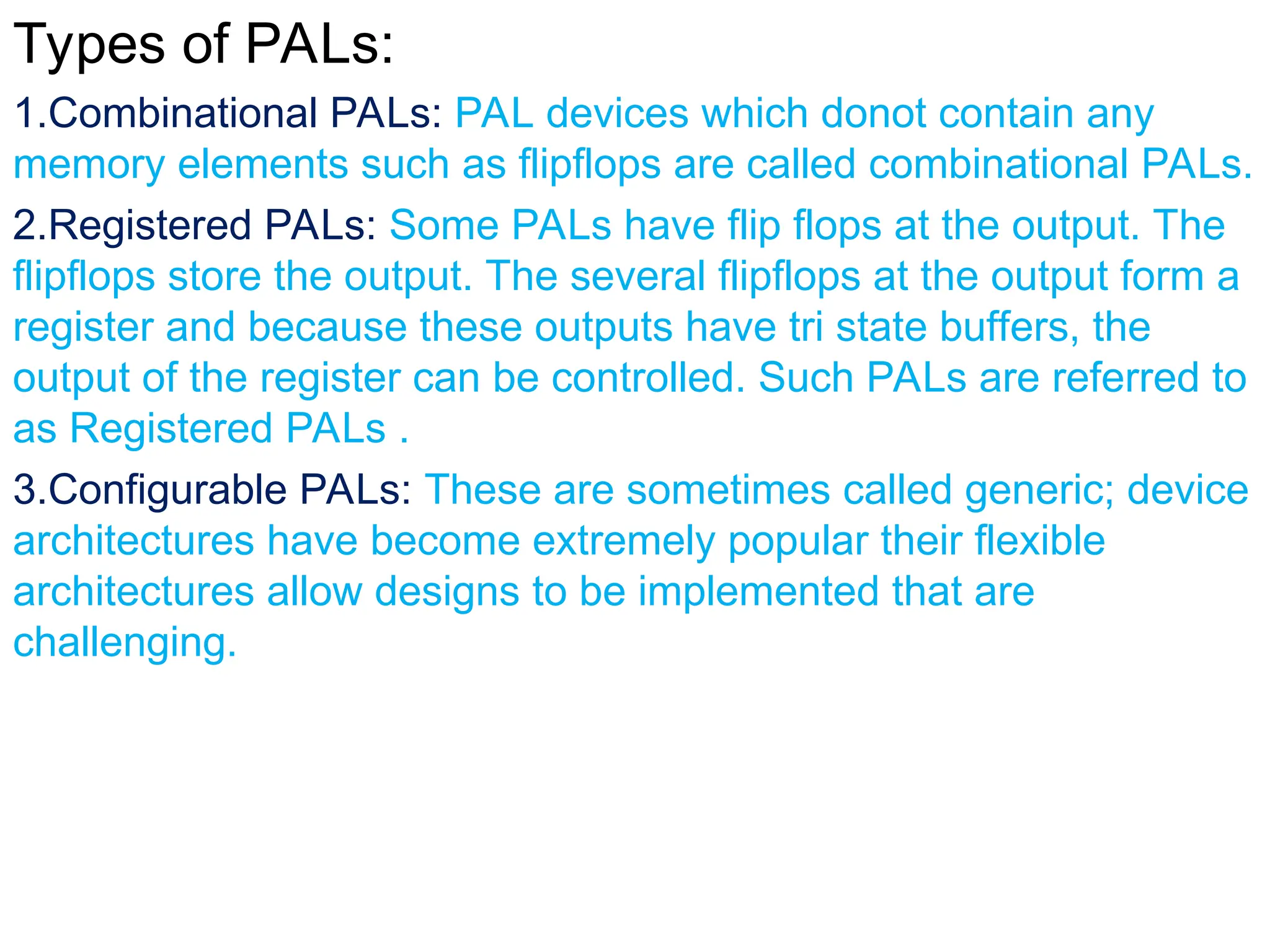
Types of PALs:
1.CombinationalPALs: PAL devices which donot contain any
memory elements such as flipflops are called combinational PALs.
2.Registered PALs: Some PALs have flip flops at the output. The
flipflops store the output. The several flipflops at the output form a
register and because these outputs have tri state buffers, the
output of the register can be controlled. Such PALs are referred to
as Registered PALs .
3.Configurable PALs: These are sometimes called generic; device
architectures have become extremely popular their flexible
architectures allow designs to be implemented that are
challenging.
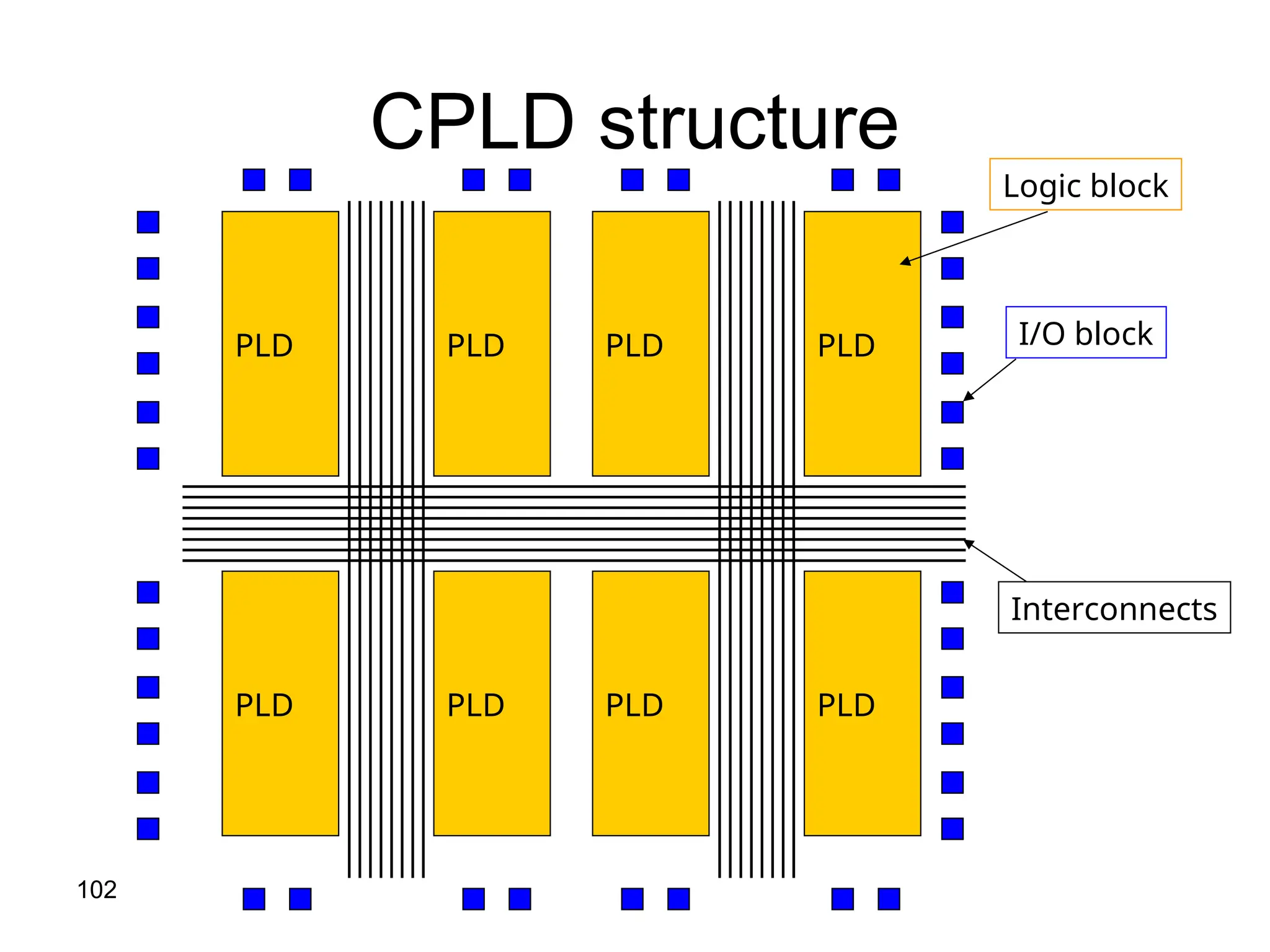
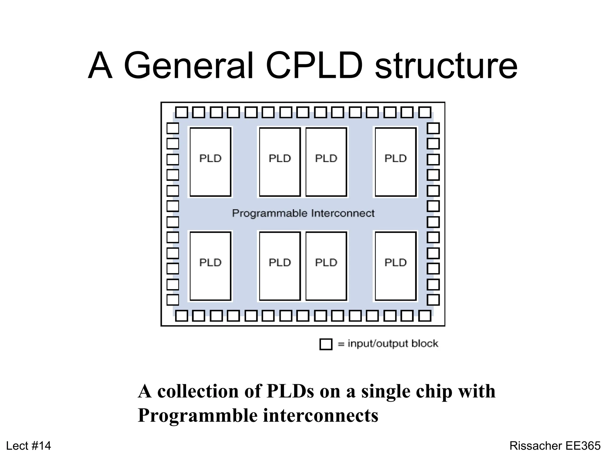
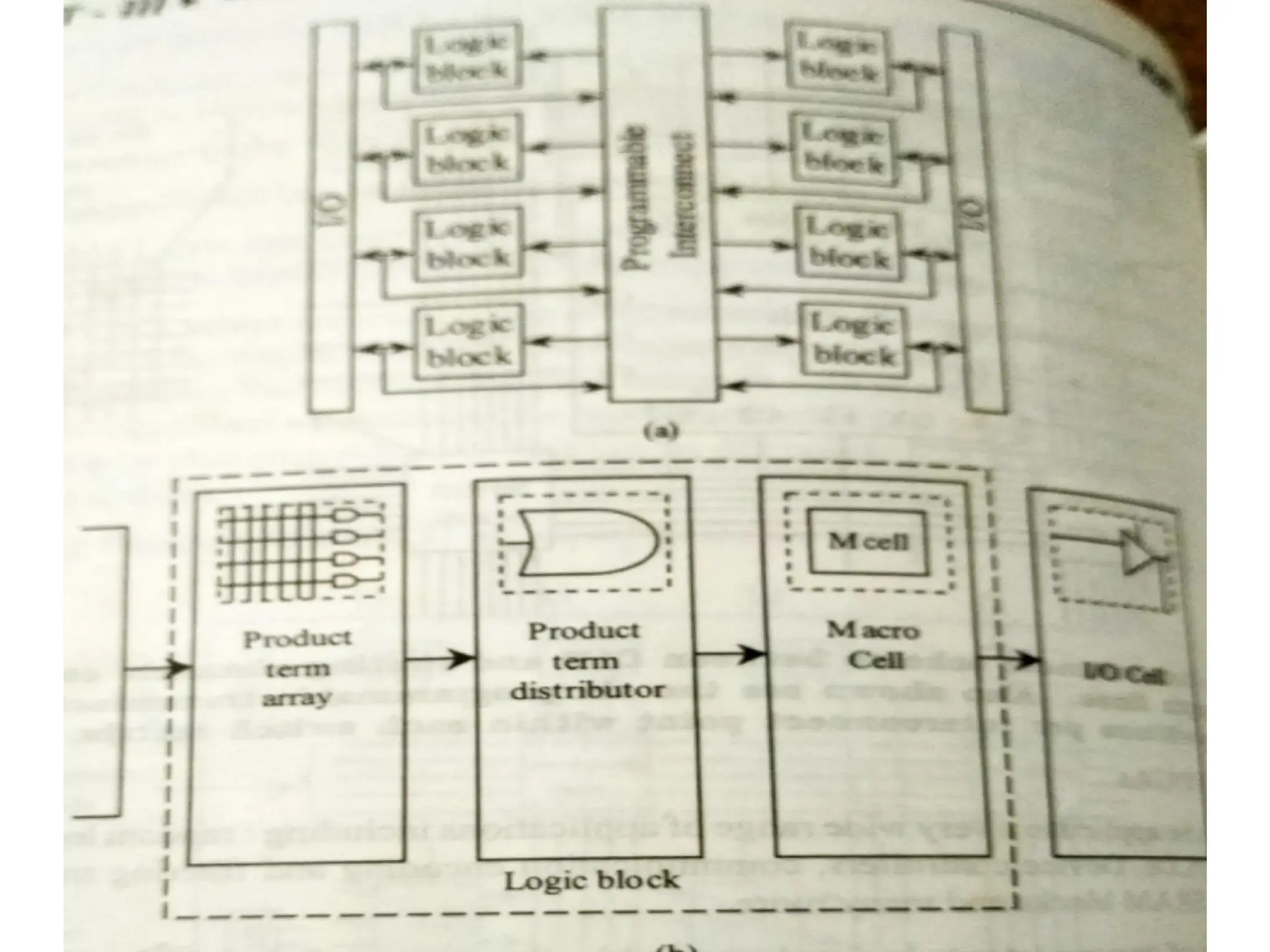
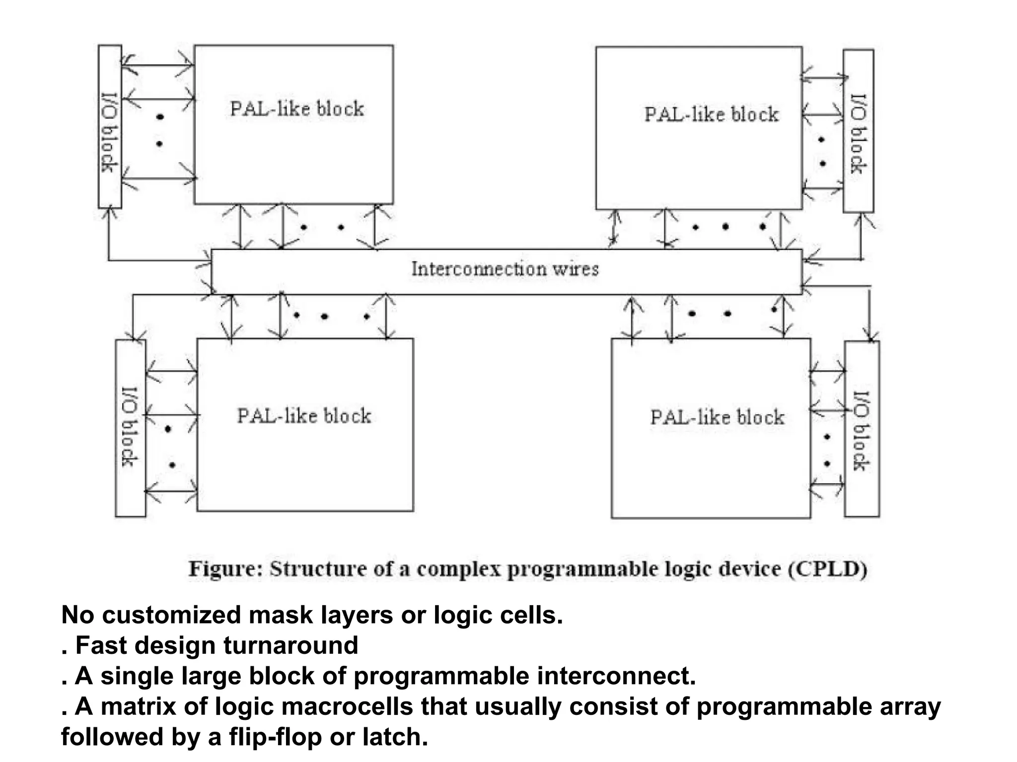
A General CPLDstructure
A collection of PLDs on a single chip with
Programmble interconnects
Rissacher EE365
Lect #14
105.
CPLD: CPLDs extendthe concept of PLD to a higher level of
integration to improve system performance ,they also use less
board space, improve reliability and reduce cost
The logic blocks communicate with each other using signals
routed via programmable interconnect.
Most CPLDs use one of the two implementations for
programmable interconnect
a.Array based b. multiplexed based
The logic block is similar to PLD each has a product term
array, a product term distribution scheme and macro cells. The
size of the logic block is measure of its capacity.
Features of CPLD include insystem programmability( ISP)
insystem reprogrammability (ISR) 5v/3.3v operation.
Test Access Port and Boundary Scan Capability device are
also offered in variety of packages
106.
No customized masklayers or logic cells.
. Fast design turnaround
. A single large block of programmable interconnect.
. A matrix of logic macrocells that usually consist of programmable array
followed by a flip-flop or latch.
107.
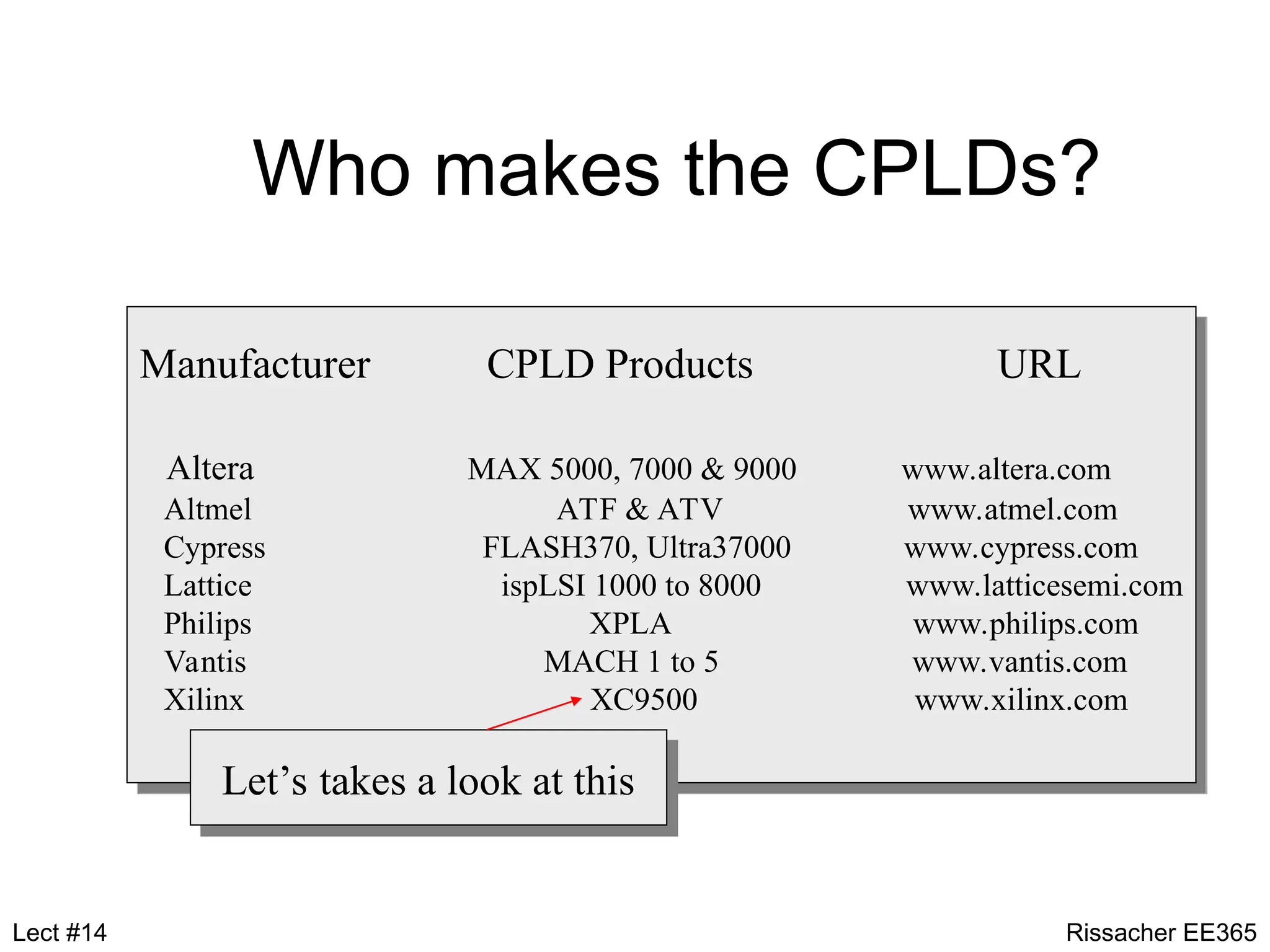
Who makes theCPLDs?
Manufacturer CPLD Products URL
Altera MAX 5000, 7000 & 9000 www.altera.com
Altmel ATF & ATV www.atmel.com
Cypress FLASH370, Ultra37000 www.cypress.com
Lattice ispLSI 1000 to 8000 www.latticesemi.com
Philips XPLA www.philips.com
Vantis MACH 1 to 5 www.vantis.com
Xilinx XC9500 www.xilinx.com
Let’s takes a look at this
Rissacher EE365
Lect #14
108.
108
CPLD and FPGA[Brown&Rose 96]
• Complex Programmable Logic Device (CPLD
CPLD)
– Multiple PLDs (e.g. PALs, PLAs) with programmable
interconnection structure
– Pioneered by Altera
• Field-Programmable Gate Array (FPGA
FPGA)
– High logic capacity with large distributed interconnection
structure
• Logic capacity number of 2-input NAND gates
– Offers more narrow logic resources
• CPLD offers logic resources w/ a wide number of inputs (AND
planes)
– Offer a higher ratio of Flip-flops to logic resources than
CPLD
• HCPLD
HCPLD (High Capacity PLD) is often used to refer
to both CPLD and FPGA
109.
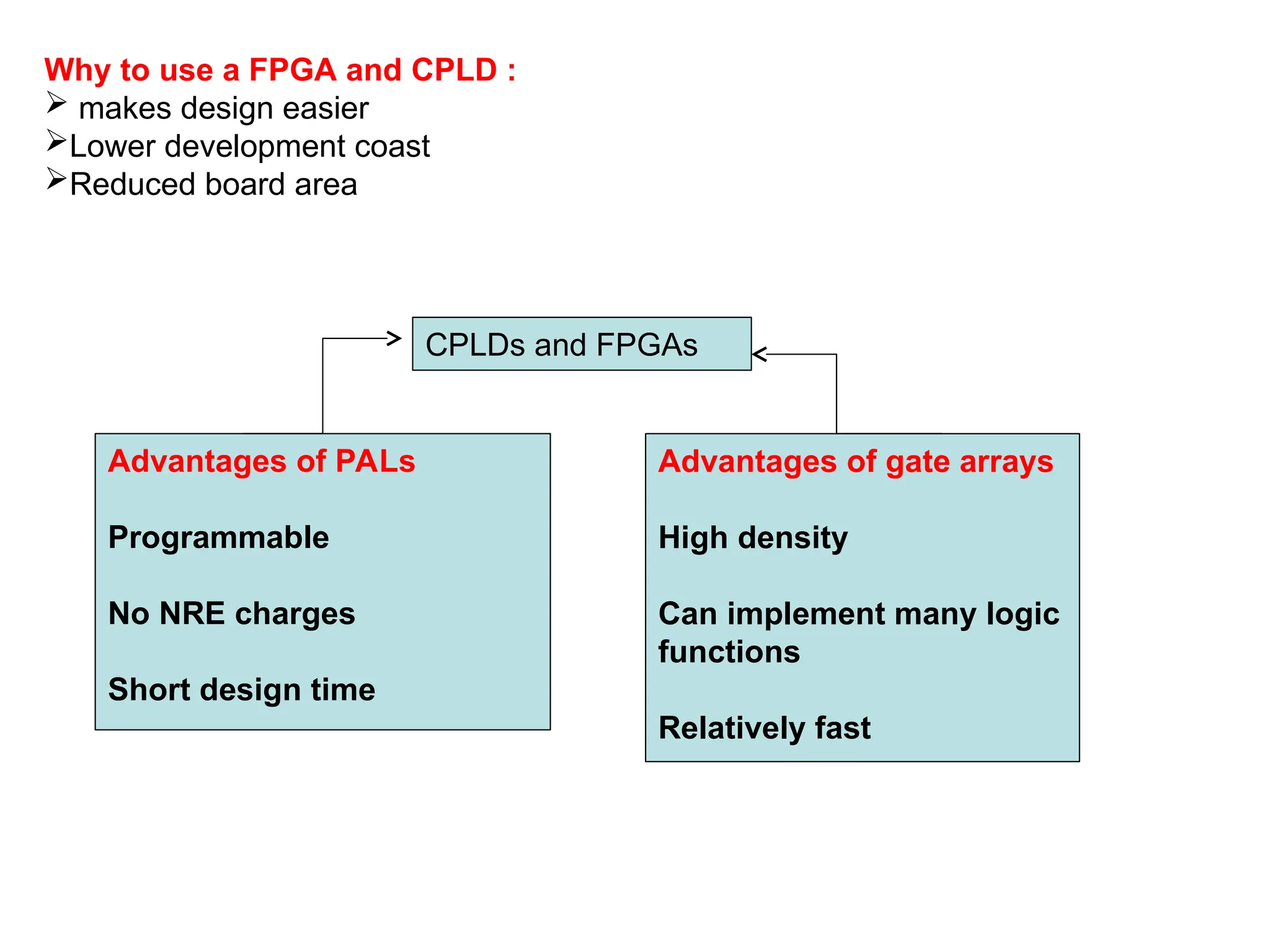
Why to usea FPGA and CPLD :
makes design easier
Lower development coast
Reduced board area
CPLDs and FPGAs
Advantages of PALs
Programmable
No NRE charges
Short design time
Advantages of gate arrays
High density
Can implement many logic
functions
Relatively fast
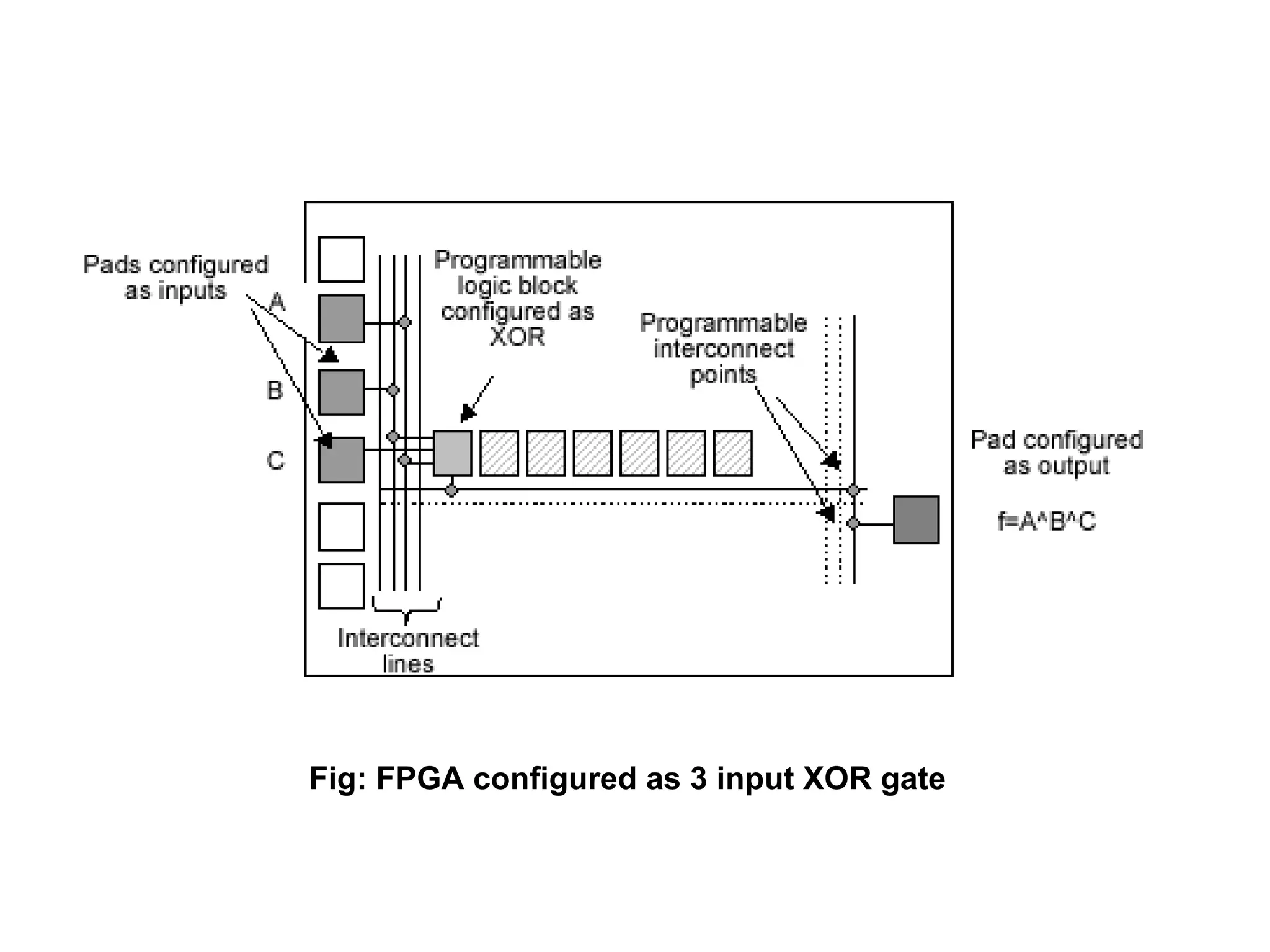
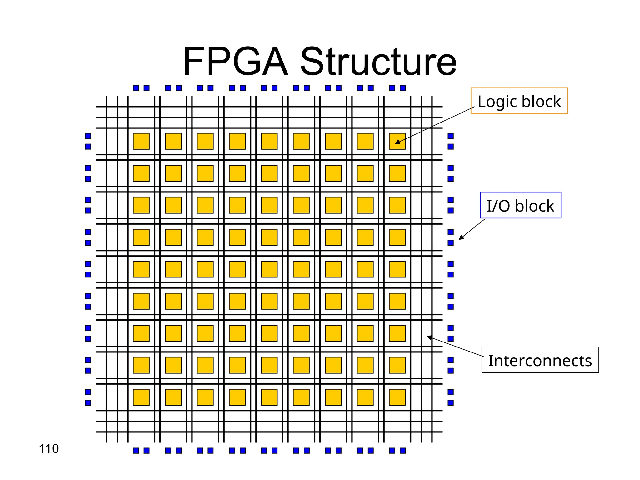
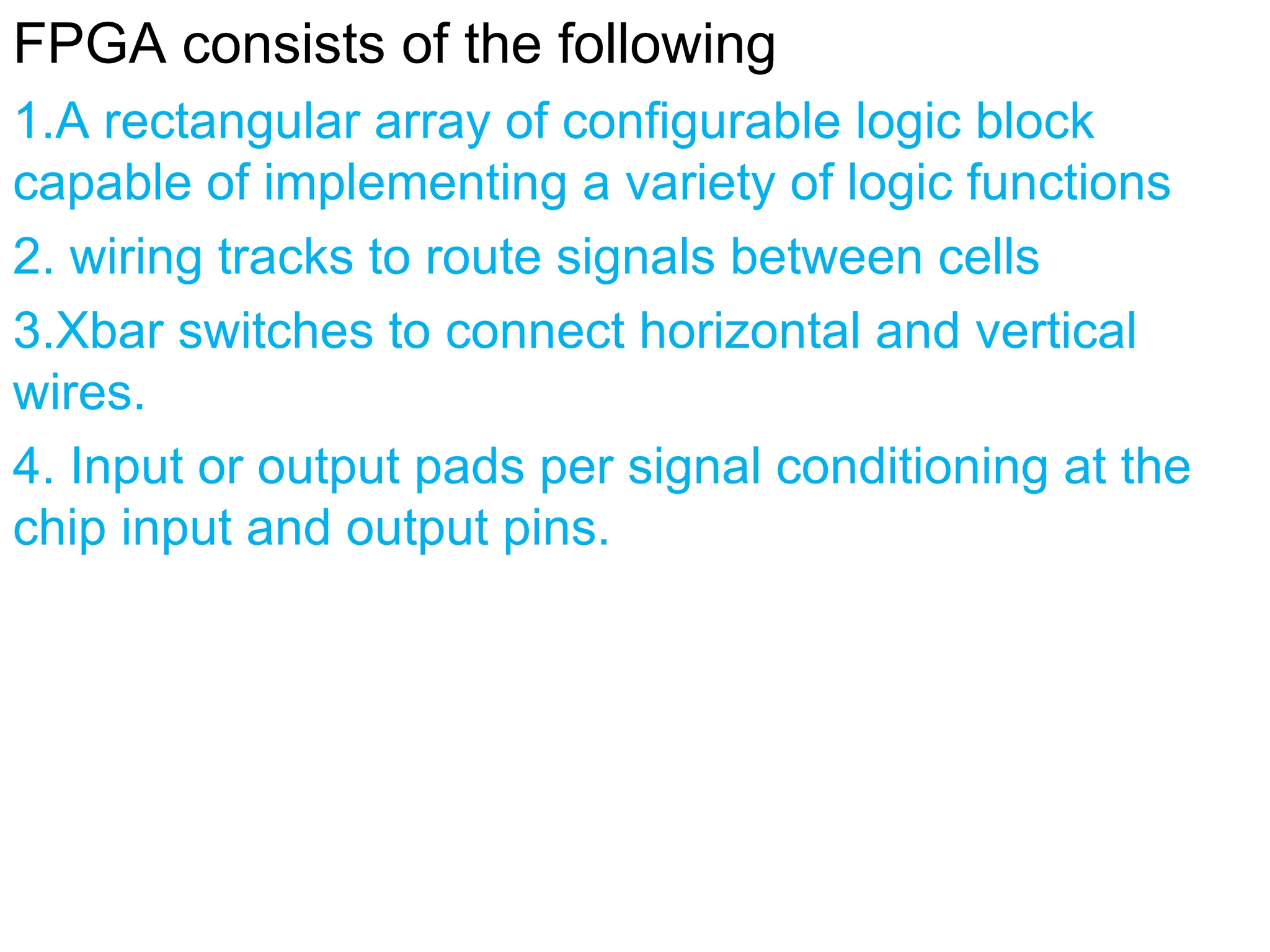
FPGA consists ofthe following
1.A rectangular array of configurable logic block
capable of implementing a variety of logic functions
2. wiring tracks to route signals between cells
3.Xbar switches to connect horizontal and vertical
wires.
4. Input or output pads per signal conditioning at the
chip input and output pins.
112.
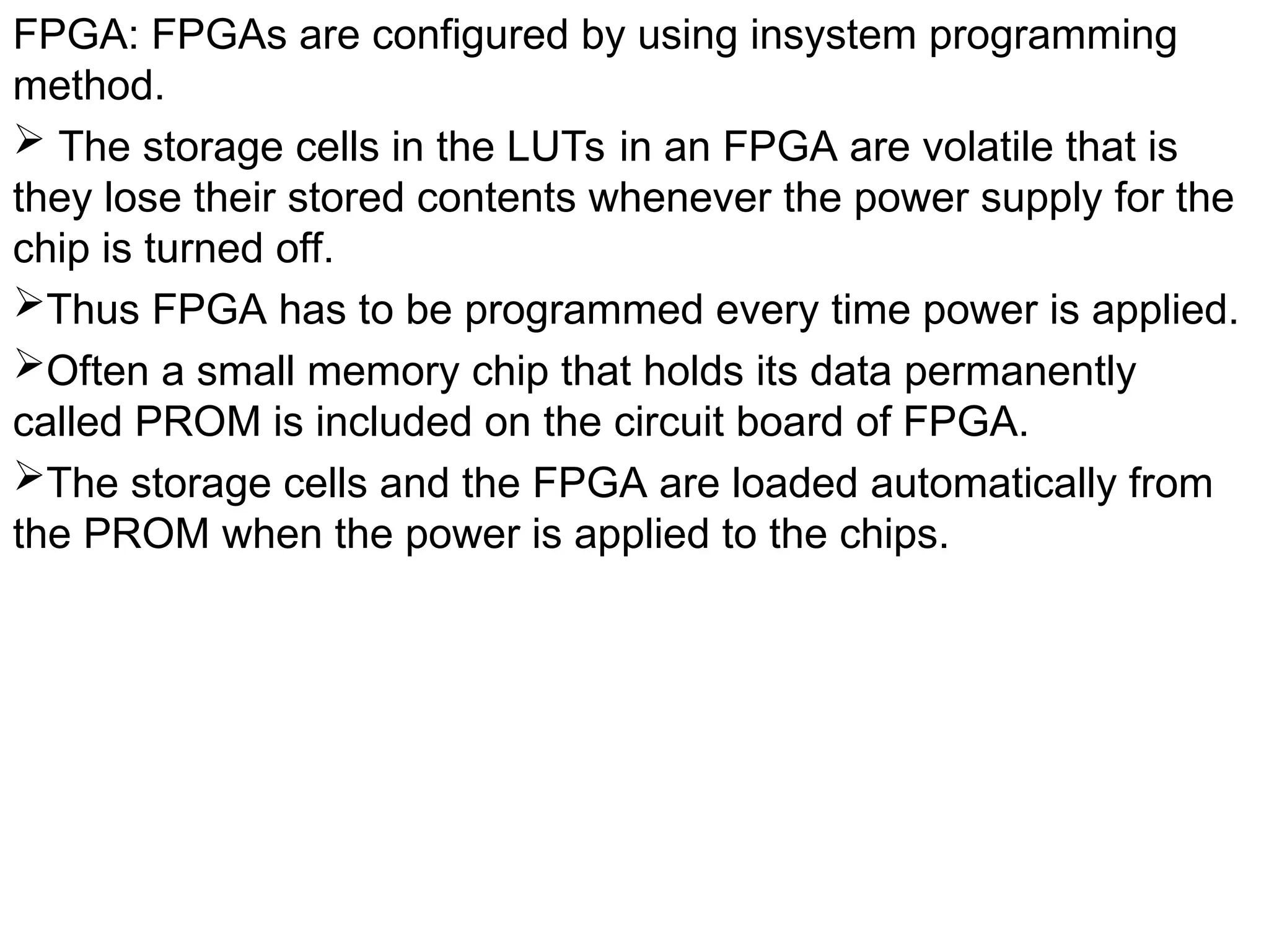
FPGA: FPGAs areconfigured by using insystem programming
method.
The storage cells in the LUTs in an FPGA are volatile that is
they lose their stored contents whenever the power supply for the
chip is turned off.
Thus FPGA has to be programmed every time power is applied.
Often a small memory chip that holds its data permanently
called PROM is included on the circuit board of FPGA.
The storage cells and the FPGA are loaded automatically from
the PROM when the power is applied to the chips.
113.
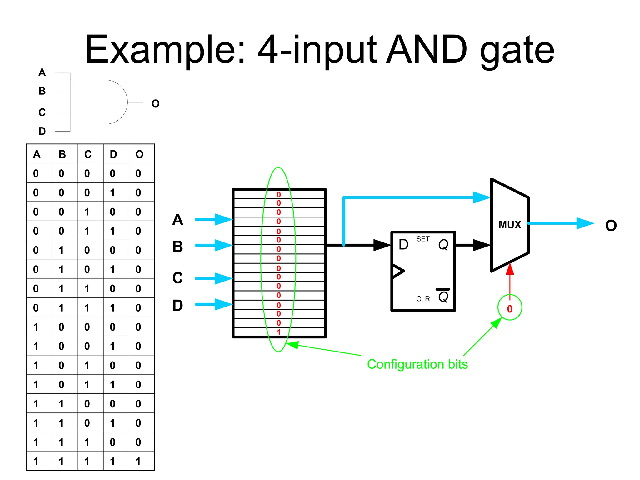
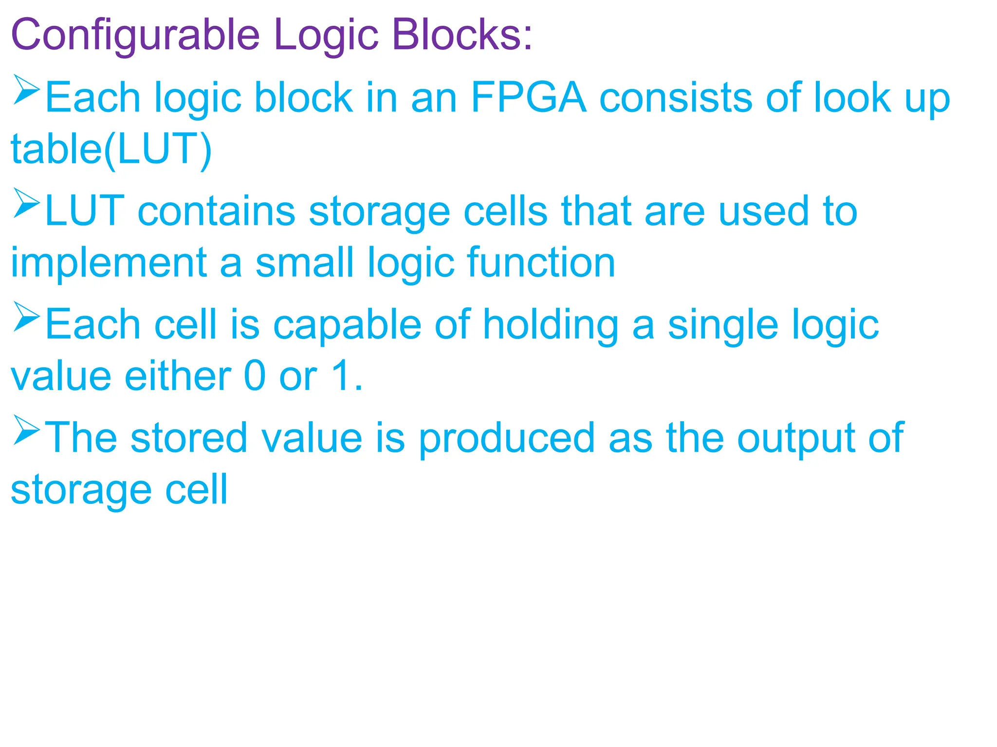
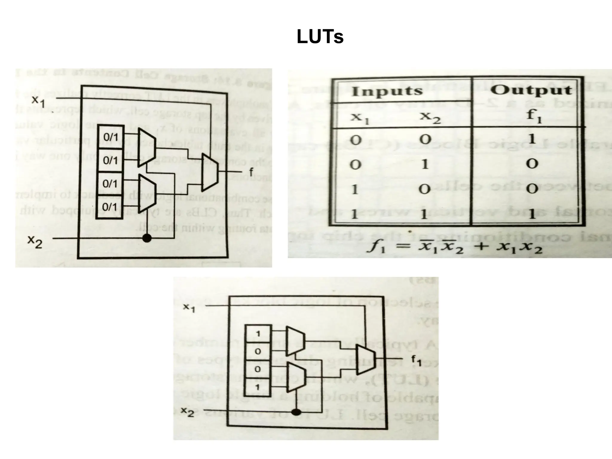
Configurable Logic Blocks:
Eachlogic block in an FPGA consists of look up
table(LUT)
LUT contains storage cells that are used to
implement a small logic function
Each cell is capable of holding a single logic
value either 0 or 1.
The stored value is produced as the output of
storage cell
Interconnect:
Routing scheme isdesigned for minimum resistance
and minimum capacitance of the average routing
paths.
There are three types of interconnects
Single length line
Double length lines
Long lines
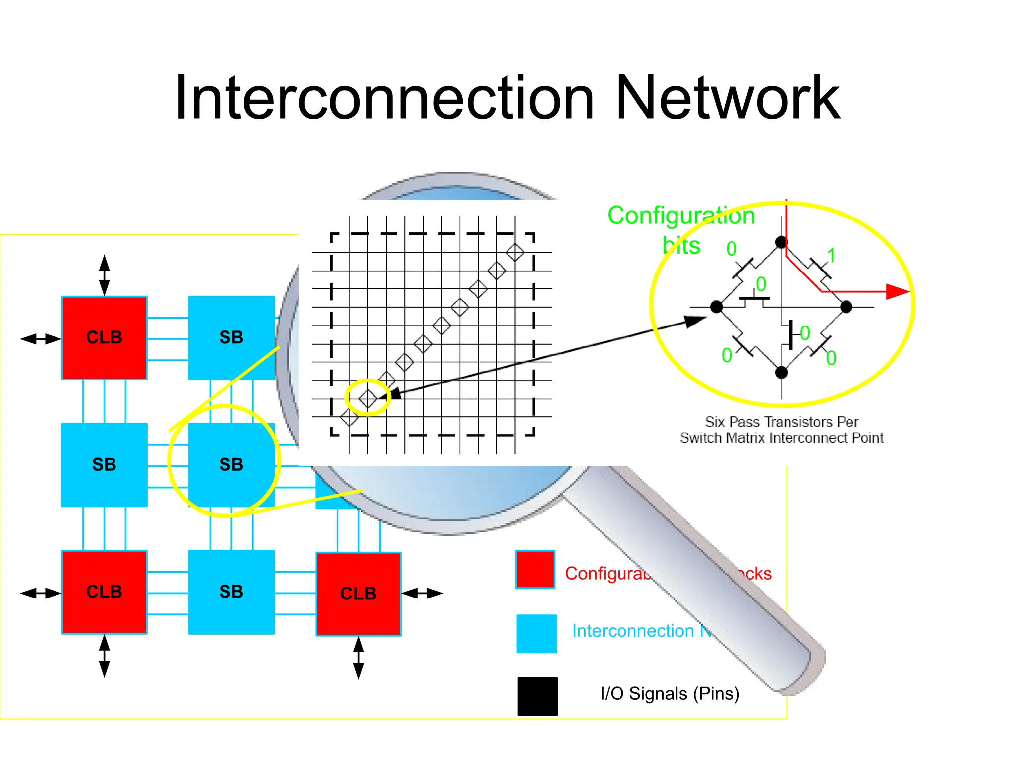
Interconnect Approaches:
1.Switch Technology
2.Anti Fuse
116.
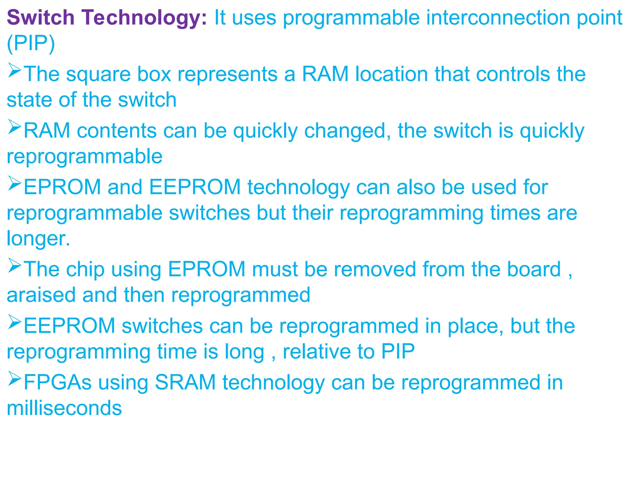
Switch Technology: Ituses programmable interconnection point
(PIP)
The square box represents a RAM location that controls the
state of the switch
RAM contents can be quickly changed, the switch is quickly
reprogrammable
EPROM and EEPROM technology can also be used for
reprogrammable switches but their reprogramming times are
longer.
The chip using EPROM must be removed from the board ,
araised and then reprogrammed
EEPROM switches can be reprogrammed in place, but the
reprogramming time is long , relative to PIP
FPGAs using SRAM technology can be reprogrammed in
milliseconds
118.
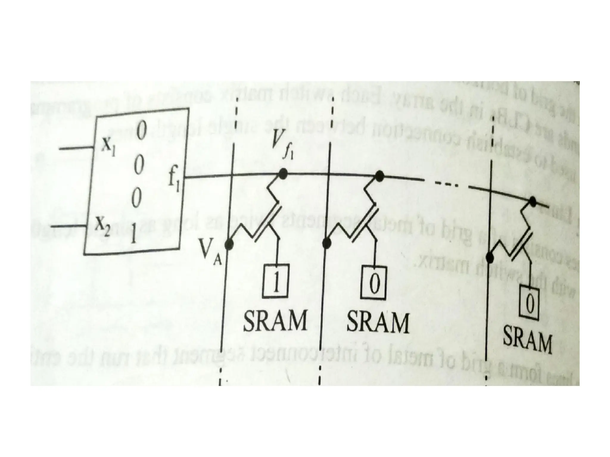
The logicblock produces a output F1 which is driven onto the
horizontal wire.
This wire can be connected to some of the vertical wires that it
crosses, using programmable switches
Each switch is implemented using an NMOS transistor with its
gate terminal controlled by the SRAM cell such a switch is
known as pass transistor switch.
If a 0 is stored in SRAM cell then the associated NMOS
transistor is turned OFF.
If a 1 is stored in SRAM cell then the NMOS transistor is turned
ON.
The switch forms a connection between the two wires attached
to its source and drain terminals.
The number of switches that are provided in the FPGA depends
on specific chip architecture.
119.
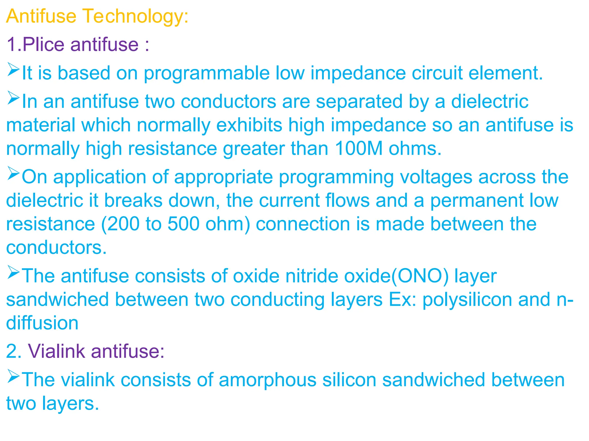
Antifuse Technology:
1.Plice antifuse:
It is based on programmable low impedance circuit element.
In an antifuse two conductors are separated by a dielectric
material which normally exhibits high impedance so an antifuse is
normally high resistance greater than 100M ohms.
On application of appropriate programming voltages across the
dielectric it breaks down, the current flows and a permanent low
resistance (200 to 500 ohm) connection is made between the
conductors.
The antifuse consists of oxide nitride oxide(ONO) layer
sandwiched between two conducting layers Ex: polysilicon and n-
diffusion
2. Vialink antifuse:
The vialink consists of amorphous silicon sandwiched between
two layers.
120.
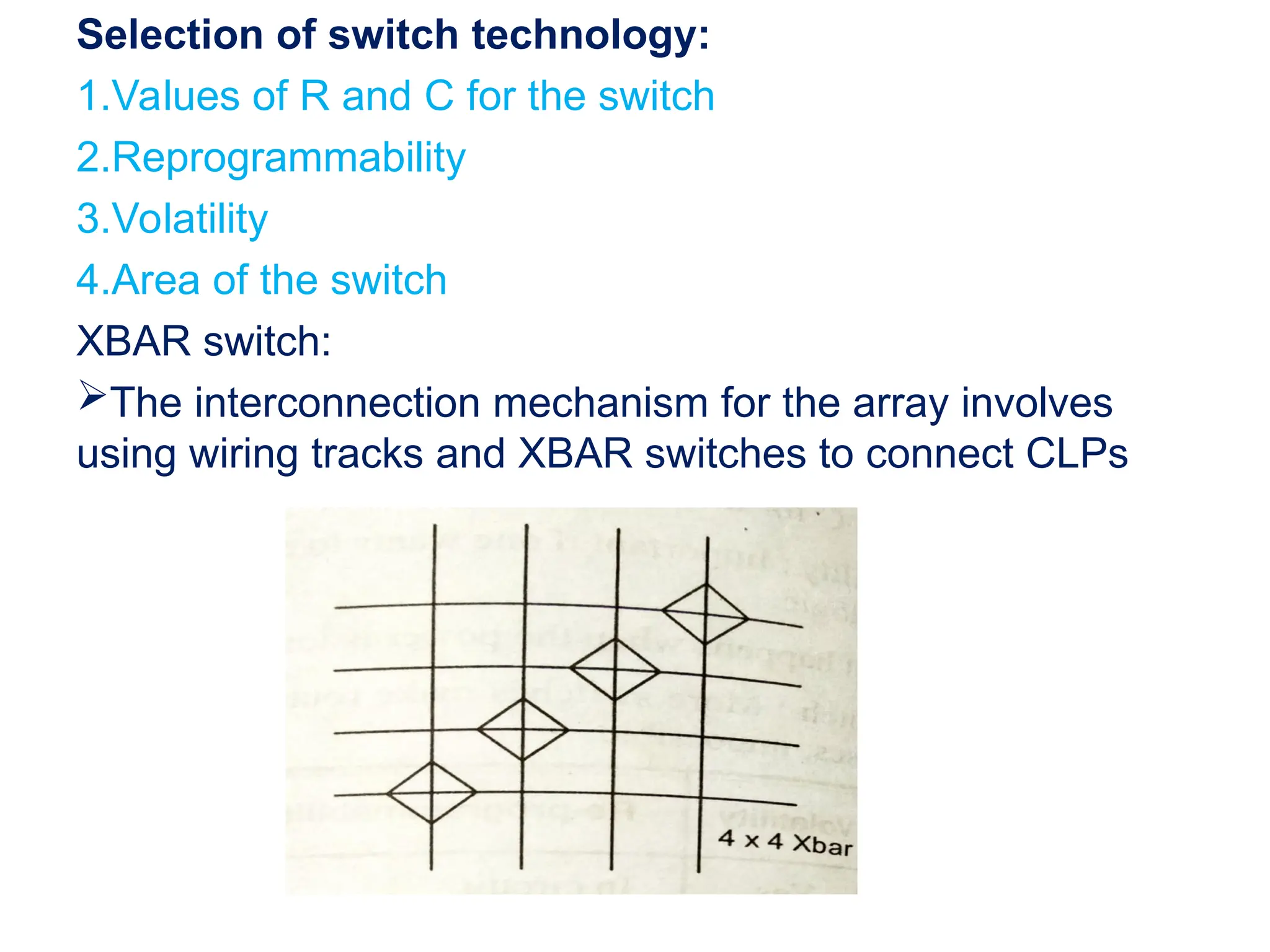
Selection of switchtechnology:
1.Values of R and C for the switch
2.Reprogrammability
3.Volatility
4.Area of the switch
XBAR switch:
The interconnection mechanism for the array involves
using wiring tracks and XBAR switches to connect CLPs
121.
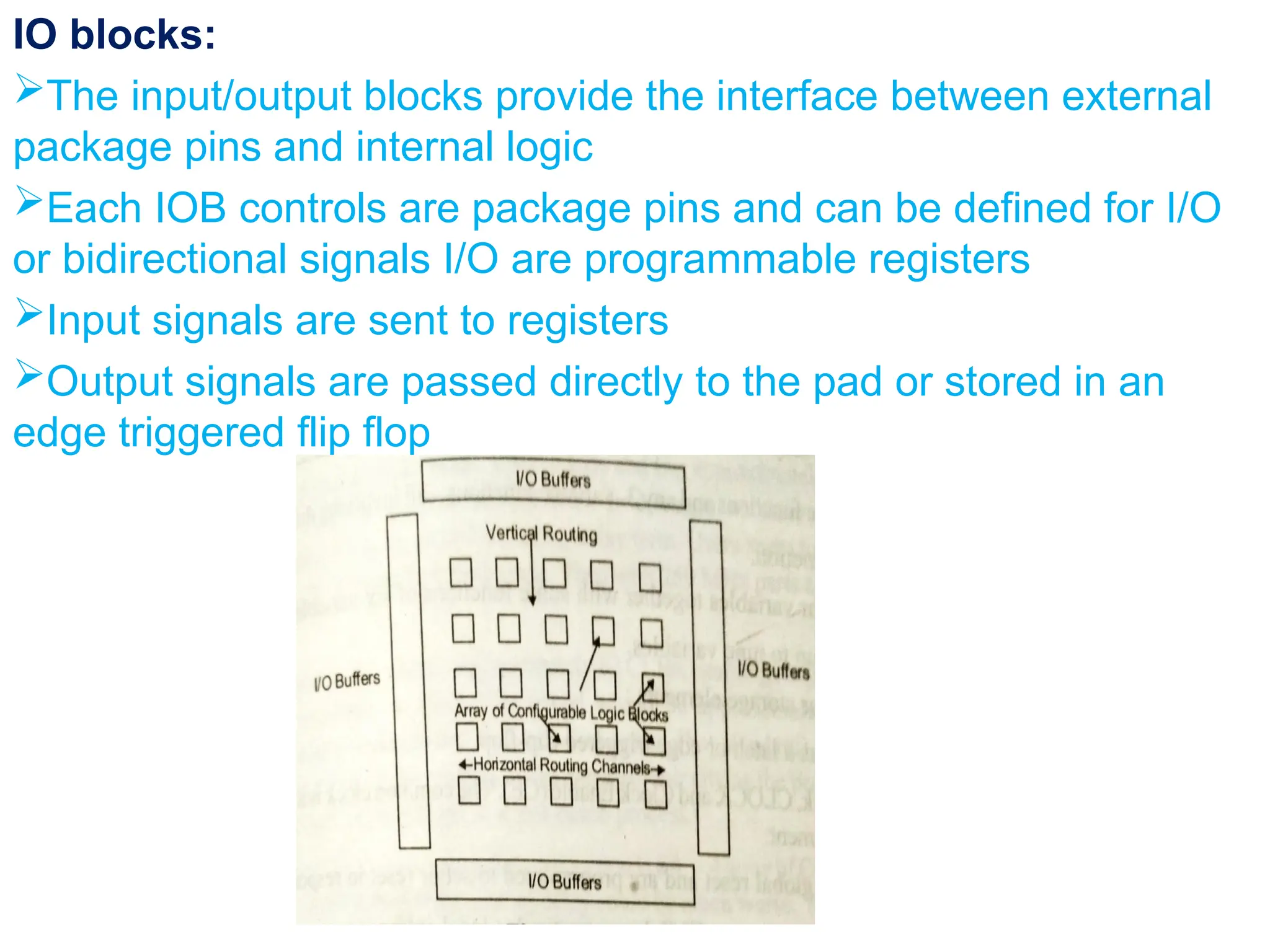
IO blocks:
The input/outputblocks provide the interface between external
package pins and internal logic
Each IOB controls are package pins and can be defined for I/O
or bidirectional signals I/O are programmable registers
Input signals are sent to registers
Output signals are passed directly to the pad or stored in an
edge triggered flip flop
122.
122
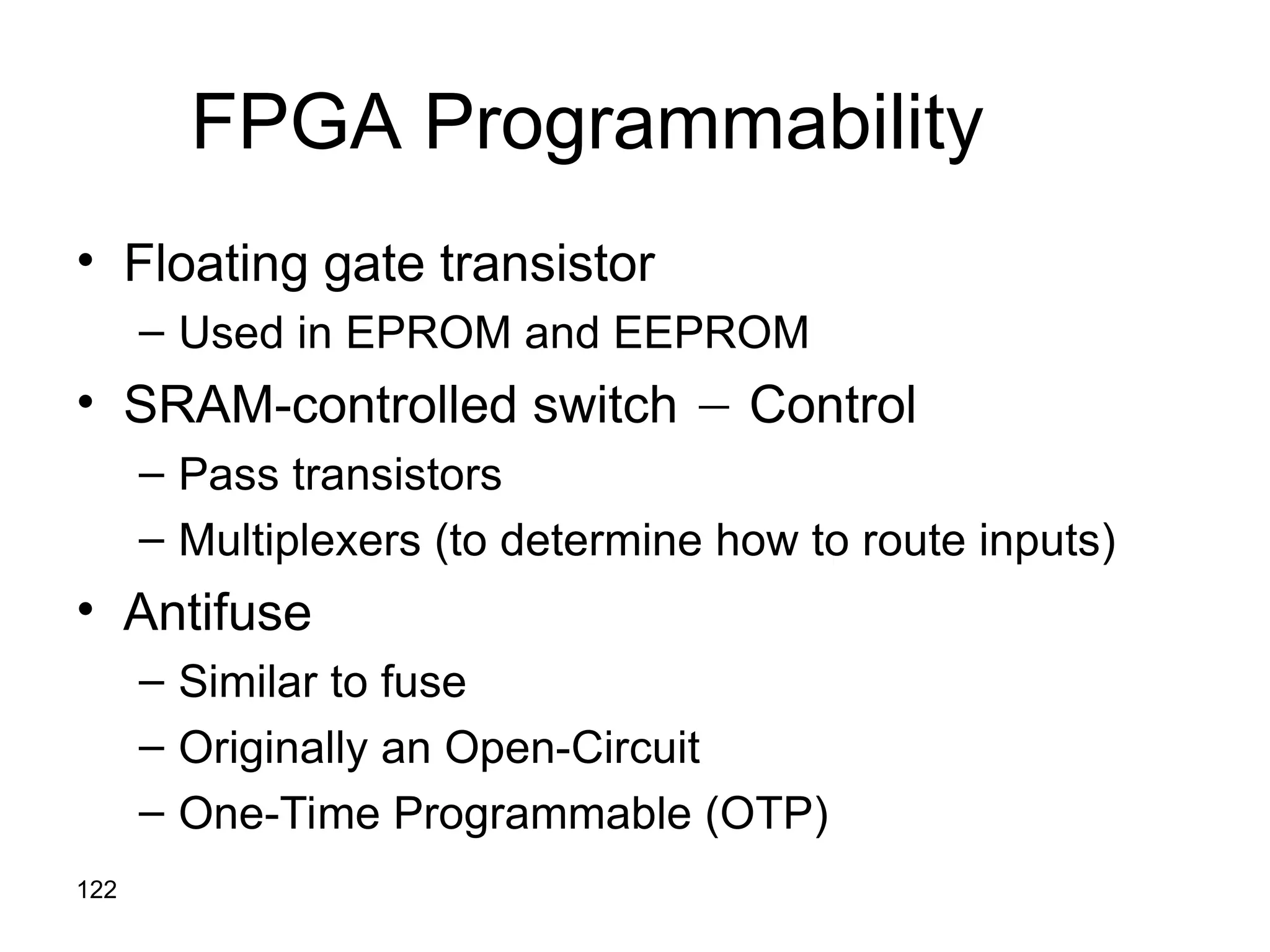
FPGA Programmability
• Floatinggate transistor
– Used in EPROM and EEPROM
• SRAM-controlled switch Control
– Pass transistors
– Multiplexers (to determine how to route inputs)
• Antifuse
– Similar to fuse
– Originally an Open-Circuit
– One-Time Programmable (OTP)
123.
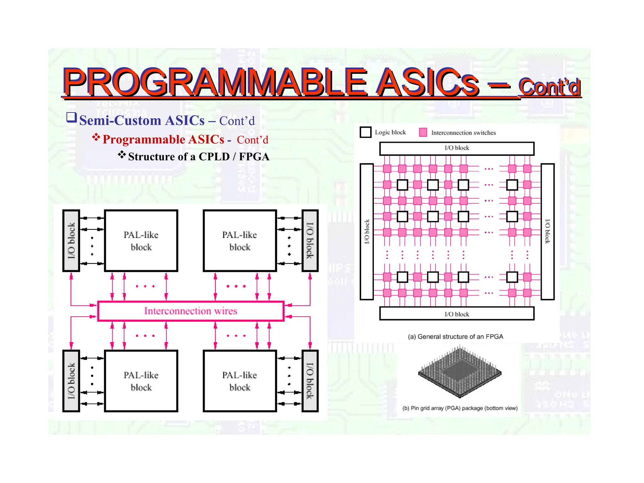
Types of ASICs–
Types of ASICs – Cont’d
Cont’d
Semi-Custom ASICs – Cont’d
Programmable ASICs
PLDs - PLDs are low-density devices
which contain 1k – 10 k gates and are
available both in bipolar and CMOS
technologies [PLA, PAL or GAL]
CPLDs or FPLDs or FPGAs -
FPGAs combine architecture of gate arrays
with programmability of PLDs.
User Configurable
Contain Regular Structures -
circuit elements such as AND, OR,
NAND/NOR gates, FFs, Mux, RAMs,
Allow Different Programming
Technologies
Allow both Matrix and Row-
based Architectures
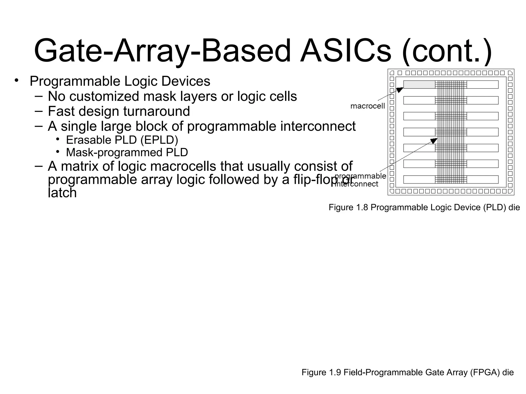
Gate-Array-Based ASICs (cont.)
Figure1.9 Field-Programmable Gate Array (FPGA) die
Figure 1.8 Programmable Logic Device (PLD) die
• Programmable Logic Devices
– No customized mask layers or logic cells
– Fast design turnaround
– A single large block of programmable interconnect
• Erasable PLD (EPLD)
• Mask-programmed PLD
– A matrix of logic macrocells that usually consist of
programmable array logic followed by a flip-flop or
latch
126.
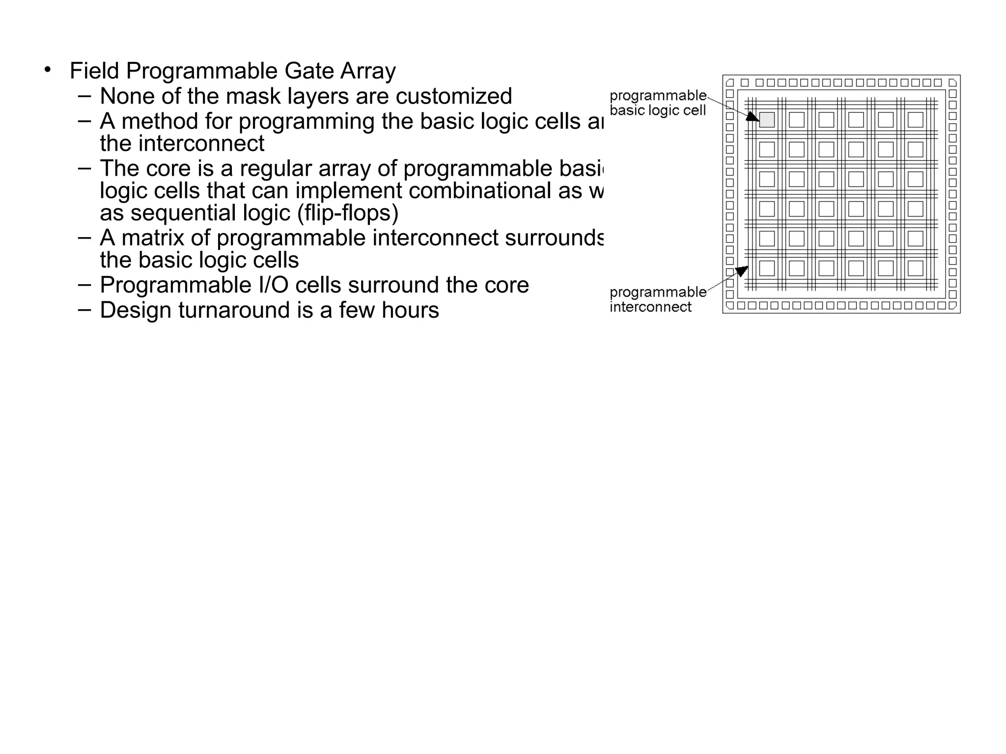
• Field ProgrammableGate Array
– None of the mask layers are customized
– A method for programming the basic logic cells and
the interconnect
– The core is a regular array of programmable basic
logic cells that can implement combinational as well
as sequential logic (flip-flops)
– A matrix of programmable interconnect surrounds
the basic logic cells
– Programmable I/O cells surround the core
– Design turnaround is a few hours
127.
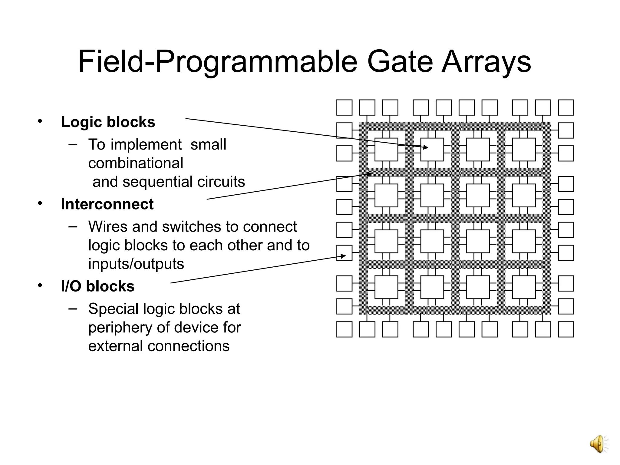
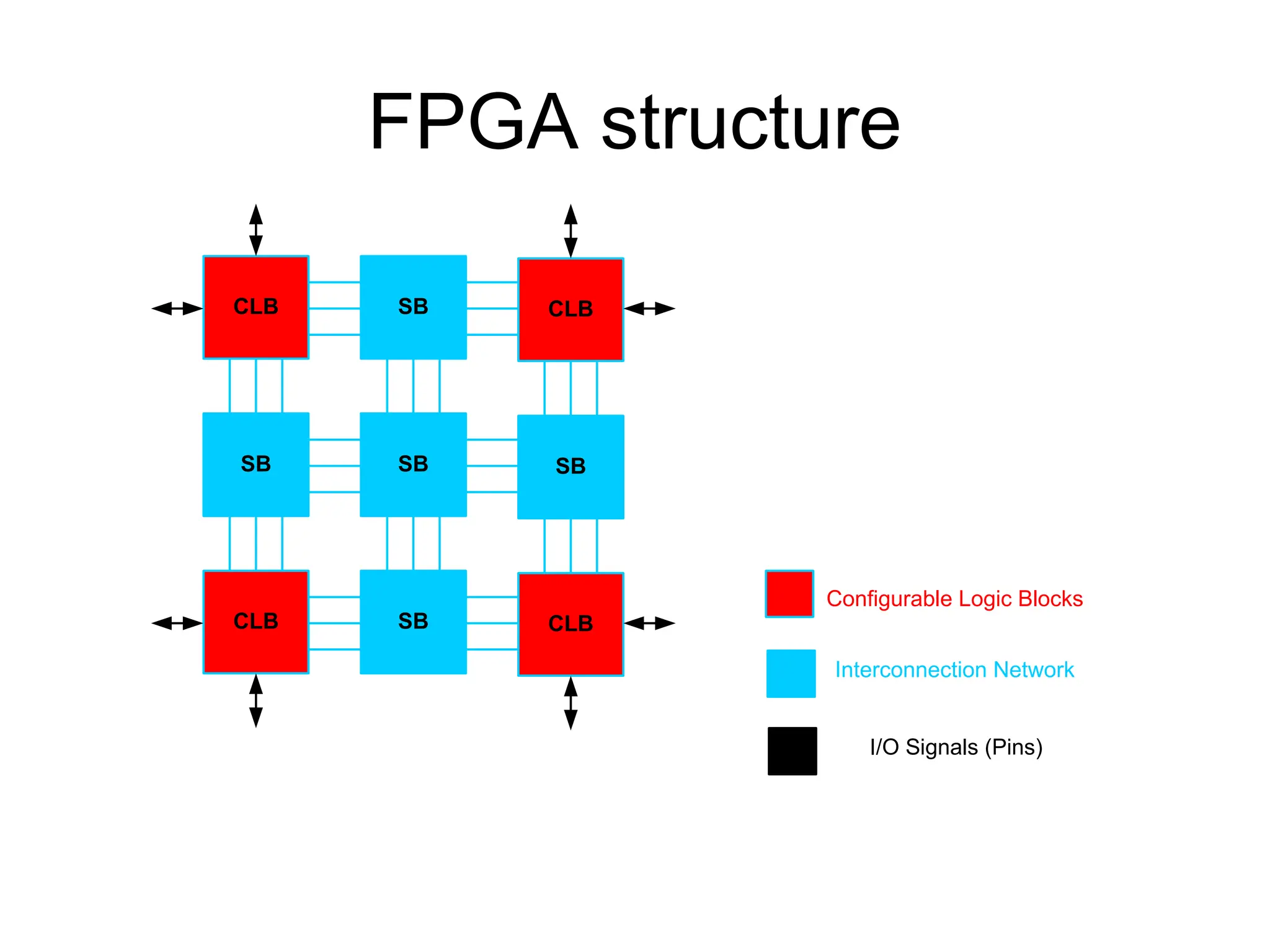
Field-Programmable Gate Arrays
•Logic blocks
– To implement small
combinational
and sequential circuits
• Interconnect
– Wires and switches to connect
logic blocks to each other and to
inputs/outputs
• I/O blocks
– Special logic blocks at
periphery of device for
external connections
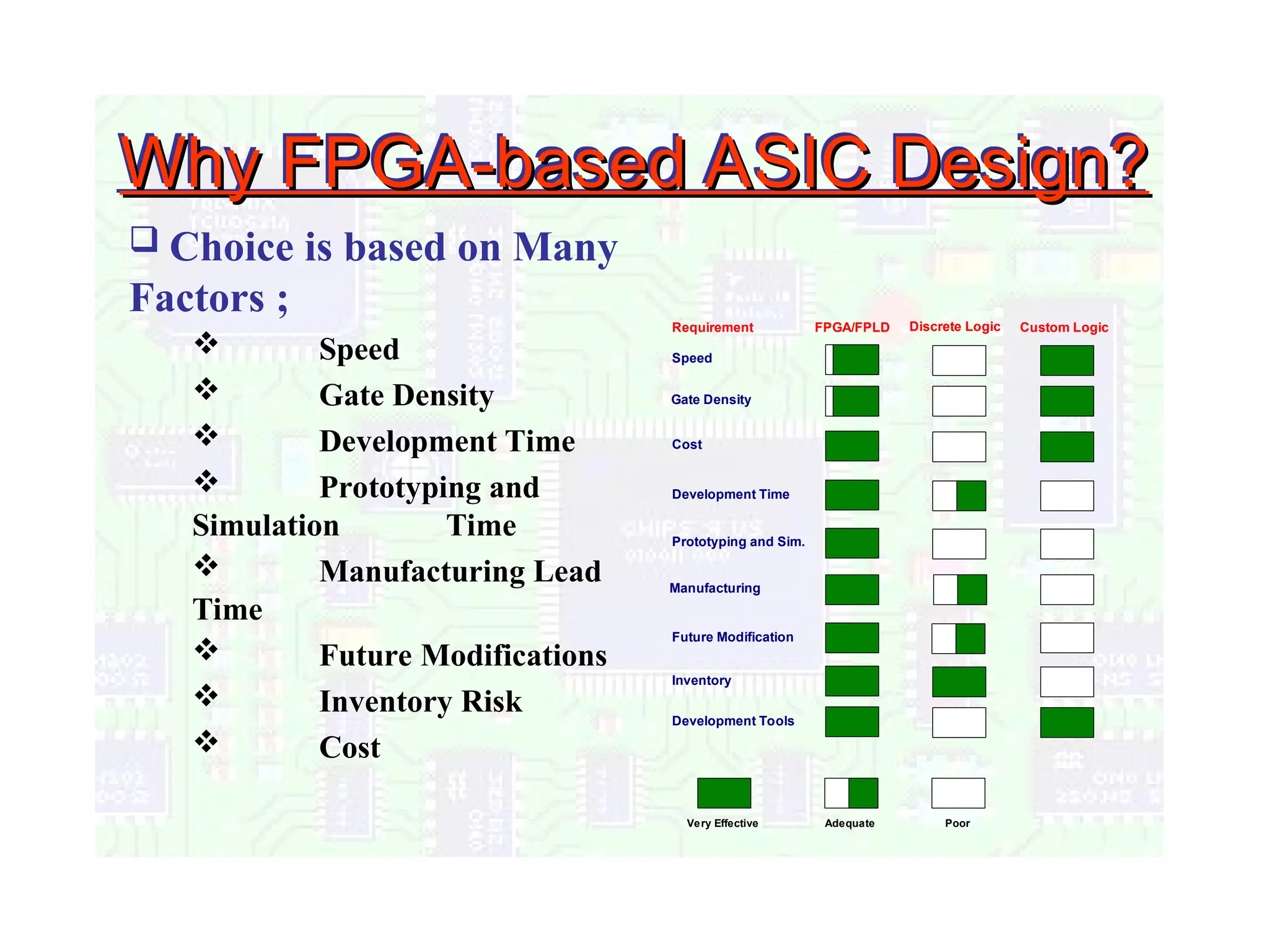
Why FPGA-based ASICDesign?
Why FPGA-based ASIC Design?
Choice is based on Many
Factors ;
Speed
Gate Density
Development Time
Prototyping and
Simulation Time
Manufacturing Lead
Time
Future Modifications
Inventory Risk
Cost
Very Effective Adequate Poor
Requirement FPGA/FPLD Discrete Logic Custom Logic
Speed
Gate Density
Cost
Development Time
Prototyping and Sim.
Manufacturing
Future Modification
Inventory
Development Tools
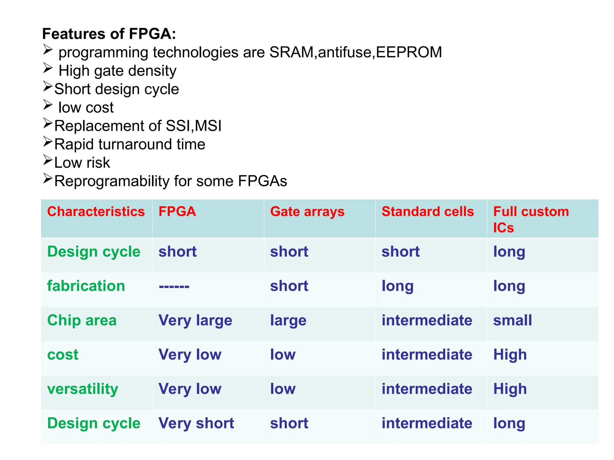
Features of FPGA:
programming technologies are SRAM,antifuse,EEPROM
High gate density
Short design cycle
low cost
Replacement of SSI,MSI
Rapid turnaround time
Low risk
Reprogramability for some FPGAs
Characteristics FPGA Gate arrays Standard cells Full custom
ICs
Design cycle short short short long
fabrication ------ short long long
Chip area Very large large intermediate small
cost Very low low intermediate High
versatility Very low low intermediate High
Design cycle Very short short intermediate long
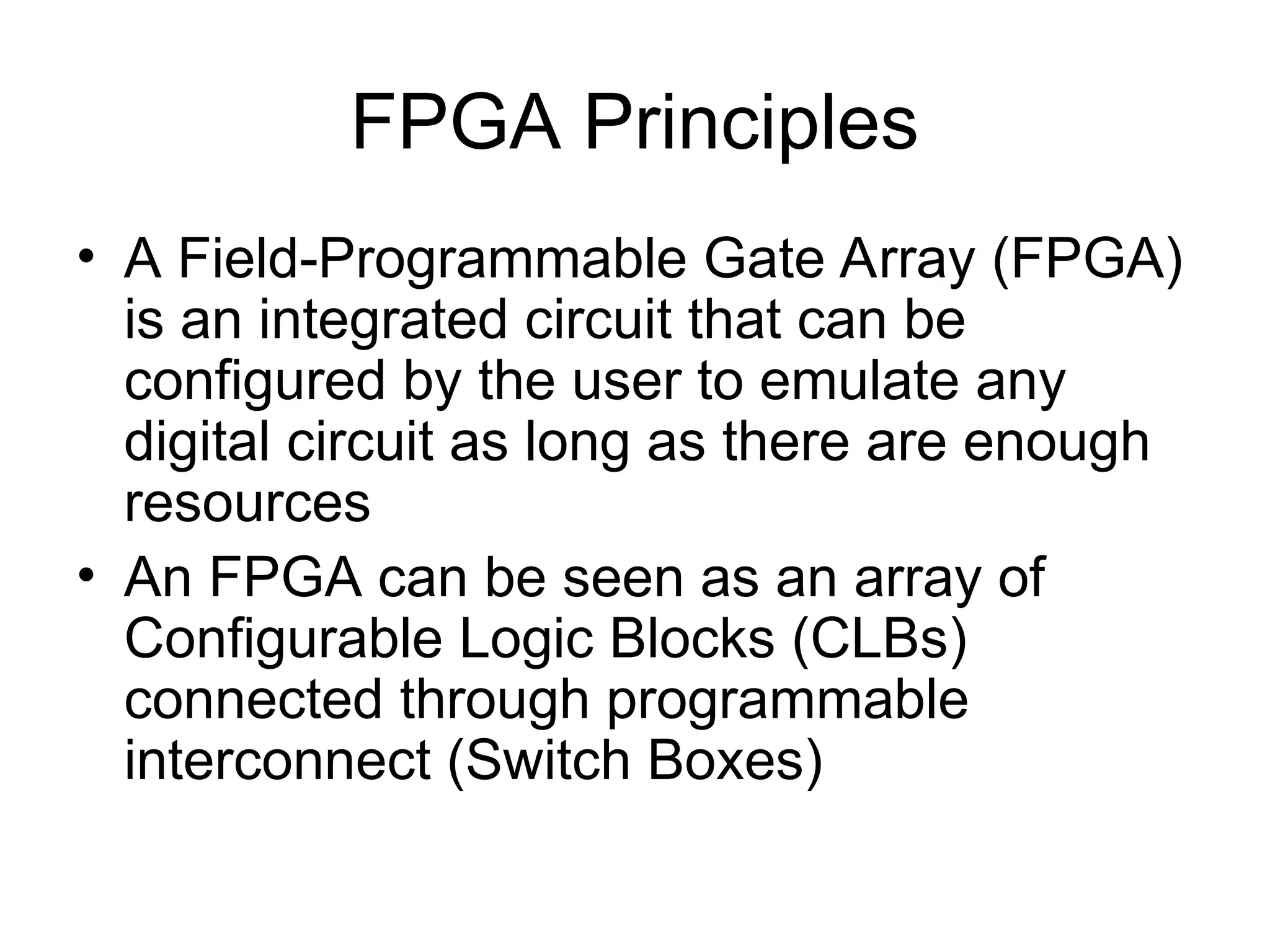
FPGA Principles
• AField-Programmable Gate Array (FPGA)
is an integrated circuit that can be
configured by the user to emulate any
digital circuit as long as there are enough
resources
• An FPGA can be seen as an array of
Configurable Logic Blocks (CLBs)
connected through programmable
interconnect (Switch Boxes)
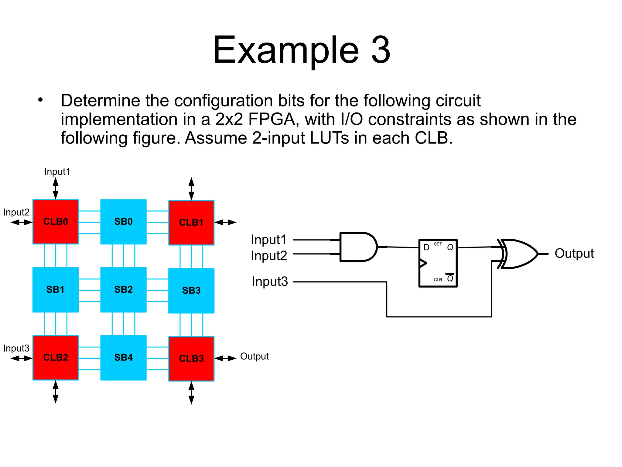
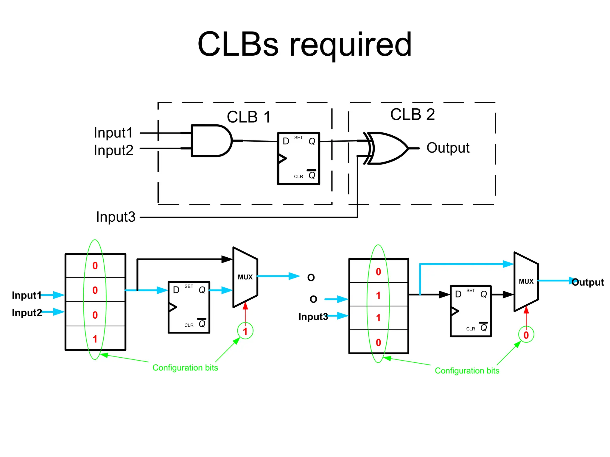
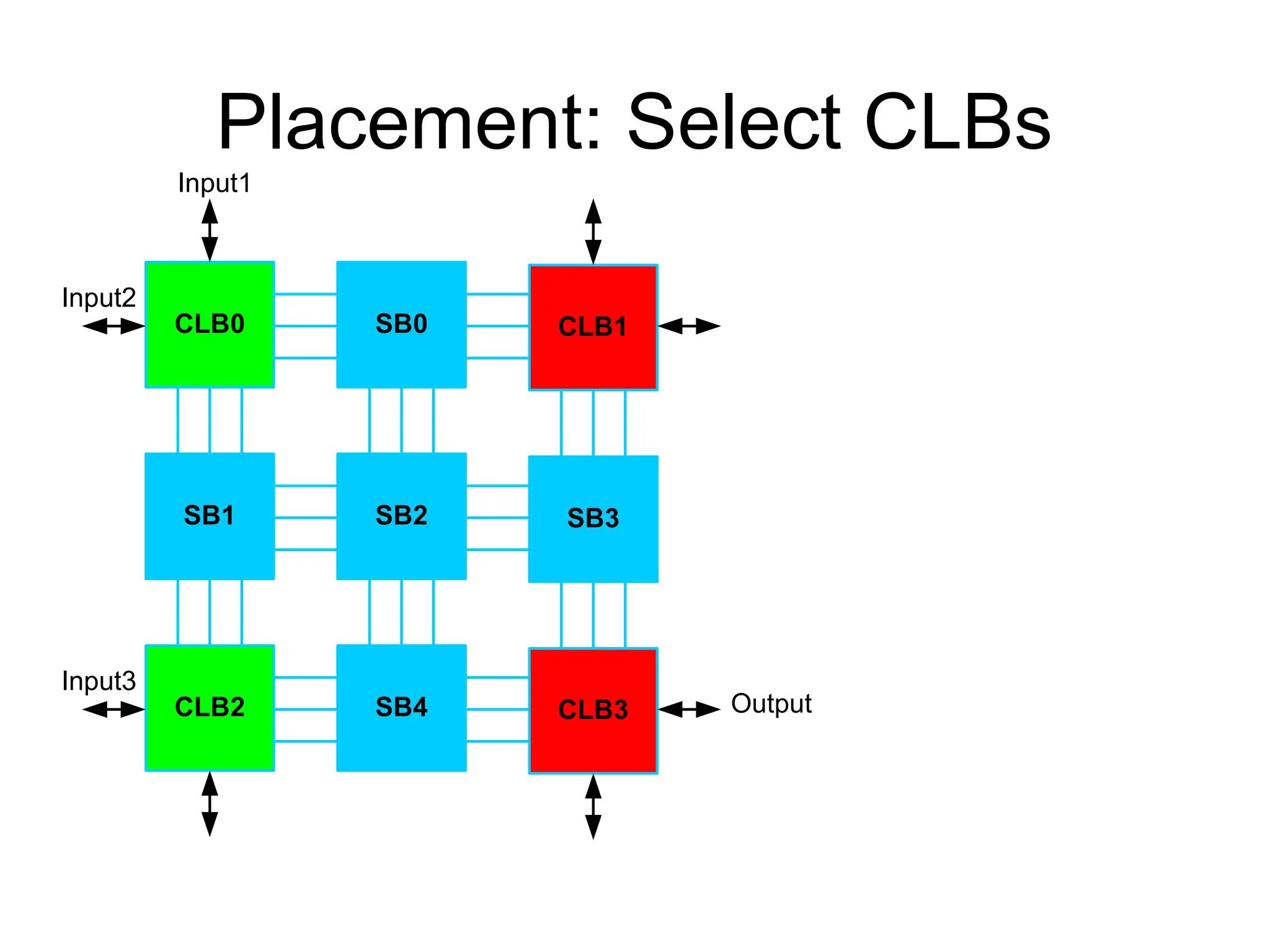
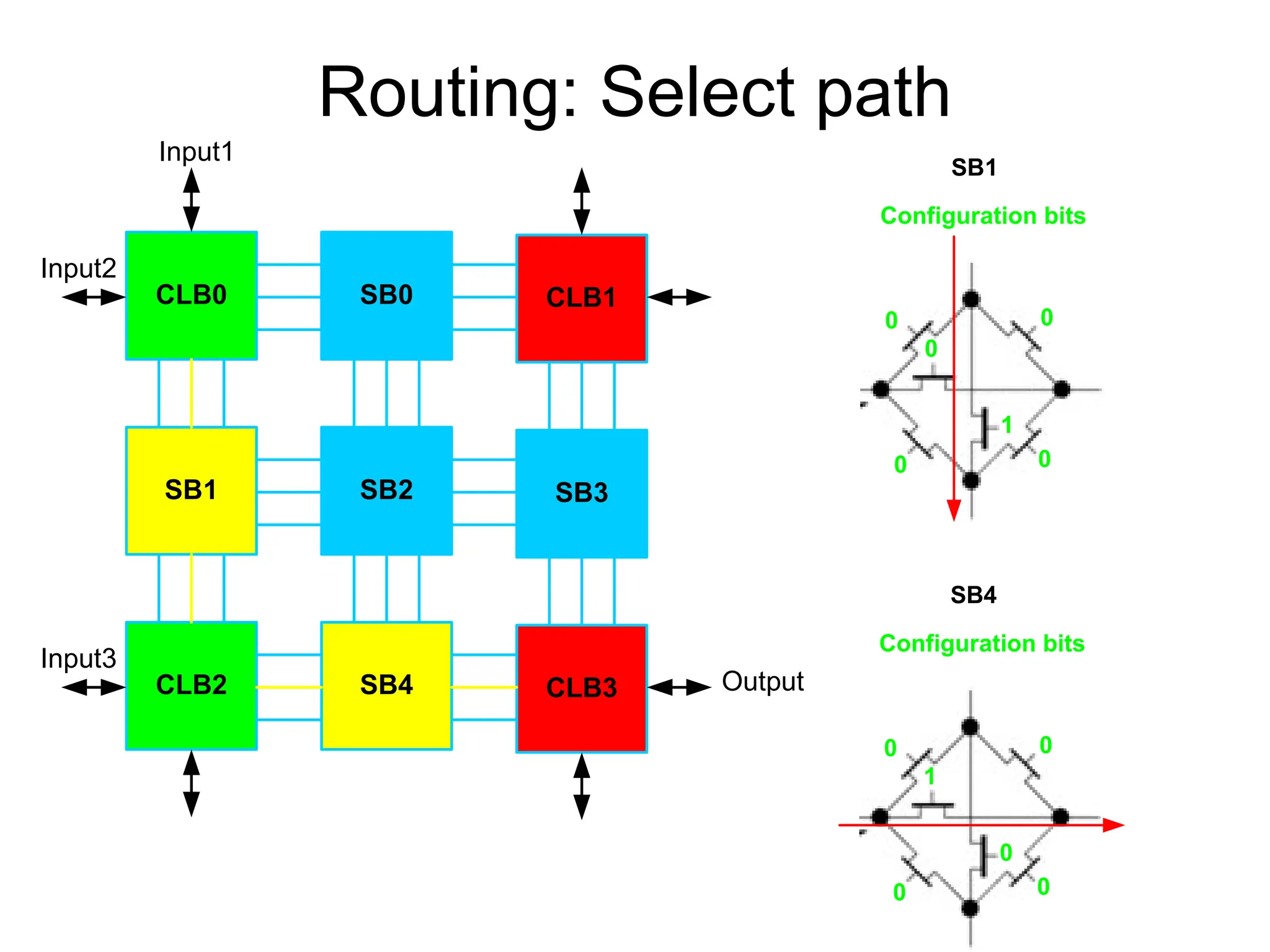
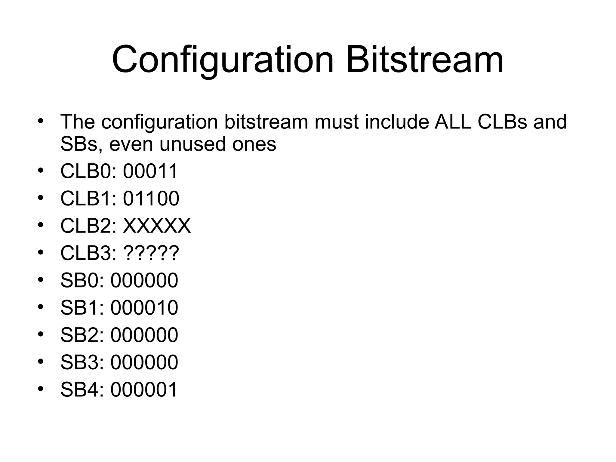
Example 3
• Determinethe configuration bits for the following circuit
implementation in a 2x2 FPGA, with I/O constraints as shown in the
following figure. Assume 2-input LUTs in each CLB.
CLB0 SB0
SB1 SB2
CLB1
SB3
CLB2 SB4 CLB3
Input1
Input2
Output
Input3
Q
Q
SET
CLR
D
Input1
Input2
Input3
Output
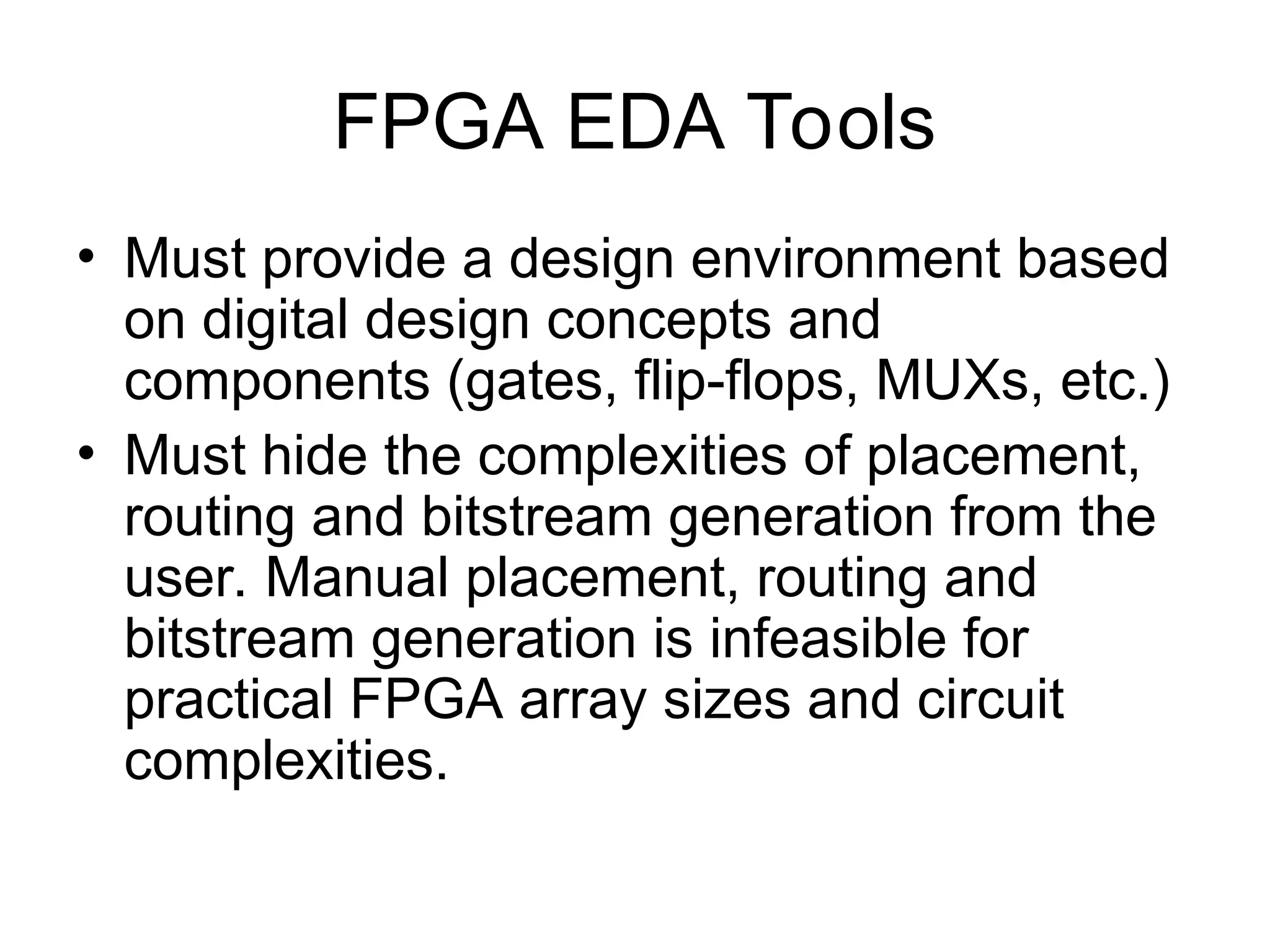
FPGA EDA Tools
•Must provide a design environment based
on digital design concepts and
components (gates, flip-flops, MUXs, etc.)
• Must hide the complexities of placement,
routing and bitstream generation from the
user. Manual placement, routing and
bitstream generation is infeasible for
practical FPGA array sizes and circuit
complexities.
146.
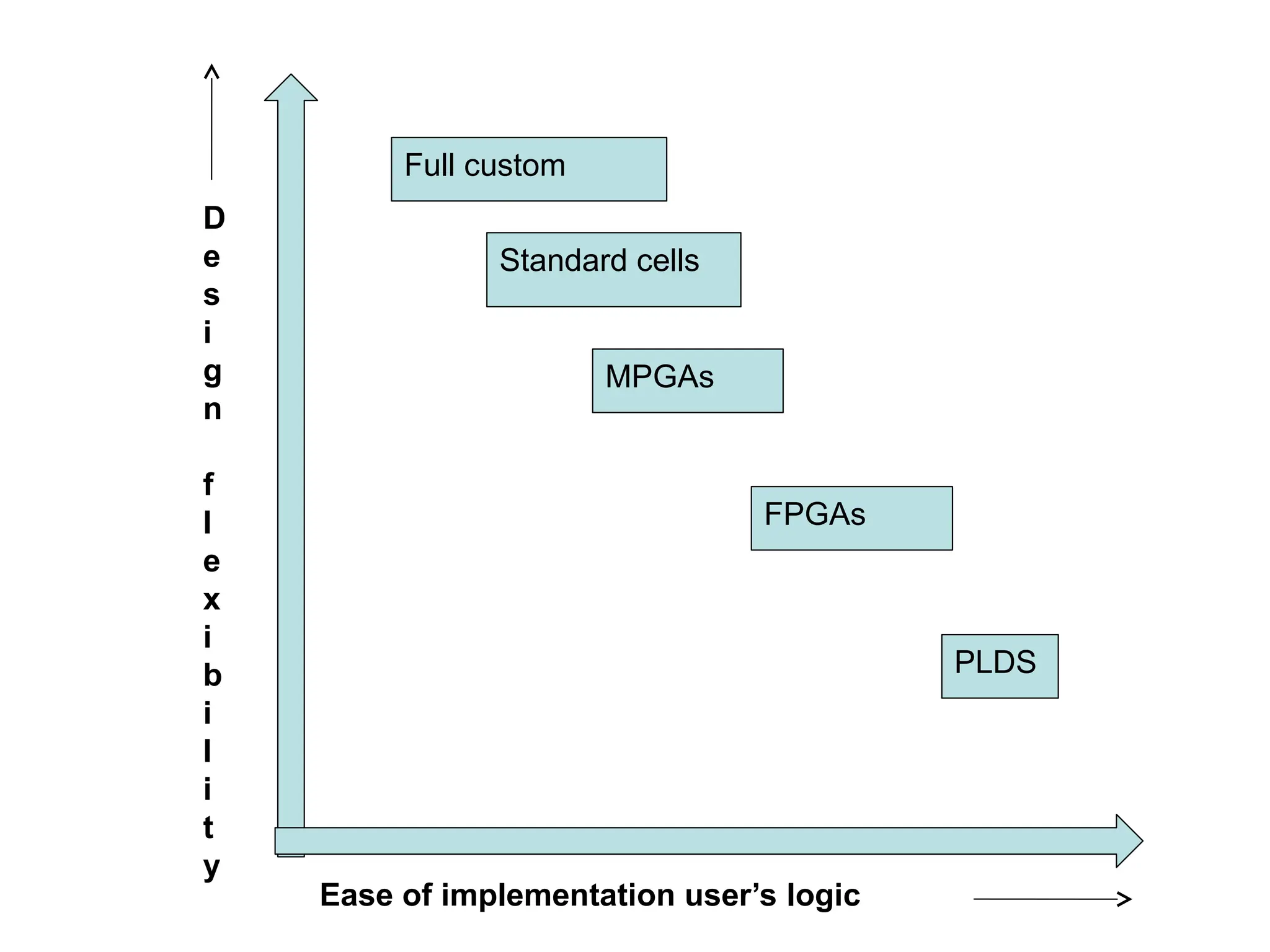
Ease of implementationuser’s logic
D
e
s
i
g
n
f
l
e
x
i
b
i
l
i
t
y
Full custom
Standard cells
MPGAs
FPGAs
PLDS
![ASIC vs Standard IC
ASIC vs Standard IC
Standard ICs – ICs sold as Standard Parts
SSI/LSI/ MSI IC such as MUX, Encoder, Memory Chips, or
Microprocessor IC
Application Specific Integrated Circuits (ASIC) –
A Chip for Toy Bear, Auto-Mobile Control Chip, Different
Communication Chips [ GRoT: ICs not Found in Data Book]
Concept Started in 1980s
An IC Customized to a Particular System or Application –
Custom ICs
Digital Designs Became a Matter of Placing of Fewer CICs
or ASICs plus Some Glue Logic
Reduced Cost and Improved Reliability
Application Specific Standard Parts (ASSP) –
Controller Chip for PC or a Modem](https://image.slidesharecdn.com/mtechvlsiunit-4-250711152449-0743a758/75/MTech-VLSI-Unit-4-ppt-details-shared-here-4-2048.jpg)


![108
CPLD and FPGA [Brown&Rose 96]
• Complex Programmable Logic Device (CPLD
CPLD)
– Multiple PLDs (e.g. PALs, PLAs) with programmable
interconnection structure
– Pioneered by Altera
• Field-Programmable Gate Array (FPGA
FPGA)
– High logic capacity with large distributed interconnection
structure
• Logic capacity number of 2-input NAND gates
– Offers more narrow logic resources
• CPLD offers logic resources w/ a wide number of inputs (AND
planes)
– Offer a higher ratio of Flip-flops to logic resources than
CPLD
• HCPLD
HCPLD (High Capacity PLD) is often used to refer
to both CPLD and FPGA](https://image.slidesharecdn.com/mtechvlsiunit-4-250711152449-0743a758/75/MTech-VLSI-Unit-4-ppt-details-shared-here-108-2048.jpg)
![Types of ASICs –
Types of ASICs – Cont’d
Cont’d
Semi-Custom ASICs – Cont’d
Programmable ASICs
PLDs - PLDs are low-density devices
which contain 1k – 10 k gates and are
available both in bipolar and CMOS
technologies [PLA, PAL or GAL]
CPLDs or FPLDs or FPGAs -
FPGAs combine architecture of gate arrays
with programmability of PLDs.
User Configurable
Contain Regular Structures -
circuit elements such as AND, OR,
NAND/NOR gates, FFs, Mux, RAMs,
Allow Different Programming
Technologies
Allow both Matrix and Row-
based Architectures](https://image.slidesharecdn.com/mtechvlsiunit-4-250711152449-0743a758/75/MTech-VLSI-Unit-4-ppt-details-shared-here-123-2048.jpg)