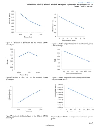
Implementation of Full Adder Cell Using High Performance CMOS Technologyijsrd.com
This paper proposed design and implementation of full adder cell which is efficient in terms of both speed and energy consumption which becomes even more significant as the world length of the adder increases. We are introducing adders for low power imprecise applications. In this we propose a full adder design having low complexity, higher computing speed, lower energy consumption, and lower operating voltage. We will explain how to realize a general full adder circuit based on transistor using CMOS technology. The performance of the proposed full adder is evaluated by the comparison of the simulation result. In this system, not signals are generated internally that control the selection of the output multiplexers. Instead, the input signal, exhibiting a full voltage swing and no extra delay, is used to drive the multiplexers, reducing the overall propagation delays. The capacitive load for the input has been reduced, as it is connected only to some transistor gates and some drain or source terminals. The design a full adder having low complexity, higher computing speed, lower energy consumption, and lower operating voltage. Full Adder models to make it understandable for designer. We are giving high throughput with less complex system by showing synthesizable and simulated results.
Low Power Full Adder using 9T Structureidescitation
In this paper, we propose a new 9T 1-bit full adder.
The main objective is full output voltage swing, low power
consumption and temperature sustainability. The proposed
design is more reliable in terms of power consumption, Power
Delay Product (PDP) and temperature sustainability as
compared to the existing full adder designs. The design has
been implemented 45nm technology on Tanner EDA Tool
version 13.0. The simulation results demonstrate the power
consumption, delay and power delay product at different input
voltages ranging 0.4V to 1.4V.
A Review of Low-Energy 1-Bit Full Adder Techniques for Power Deprived Applica...ijsrd.com
In this work a comparison and study of different low power 1-bit full adder techniques at deep submicron technologies is carried out. The study concentrates in the crucial factors which determine the applicability of the design for particular applications. The comparison of different adders has been carried out on the basis of these parameters i.e. delay, power consumption, output swing, PDP etc. The comparison is carried out between designs with low device count. On the basis of comparison a conclusion has been drawn in which the shortcomings of present designs have been discussed with future possibilities of improvement. The designs compared are TGA, SERF and modified SERF.
LOW POWER SI CLASS E POWER AMPLIFIER AND RF SWITCH FOR HEALTH CAREieijjournal
This research was to design a 2.4 GHz class E Power Amplifier (PA) for health care, with 0.18um
Semiconductor Manufacturing International Corporation CMOS technology by using Cadence software.
And also RF switch was designed at cadence software with power Jazz 180nm SOI process. The ultimate
goal for such application is to reach high performance and low cost, and between high performance and
low power consumption design. This paper introduces the design of a 2.4GHz class E power amplifier and RF switch design. PA consists of cascade stage with negative capacitance. This power amplifier can transmit 16dBm output power to a 50Ω load. The performance of the power amplifier and switch meet the specification requirements of the desired.
Review on Design and Performance Analysis of Low Power Transceiver Circuit in...iosrjce
IOSR Journal of Electronics and Communication Engineering(IOSR-JECE) is a double blind peer reviewed International Journal that provides rapid publication (within a month) of articles in all areas of electronics and communication engineering and its applications. The journal welcomes publications of high quality papers on theoretical developments and practical applications in electronics and communication engineering. Original research papers, state-of-the-art reviews, and high quality technical notes are invited for publications.
A Two Channel Analog Front end Design AFE Design with Continuous Time ∑-∆ Mod...IJECEIAES
In this context, the AFE with 2-channels is described, which has high impedance for low power application of bio-medical electrical activity. The challenge in obtaining accurate recordings of biomedical signals such as EEG/ECG to study the human body in research work. This paper is to propose Multi-Vt in AFE circuit design cascaded with CT modulator. The new architecture is anticipated with two dissimilar input signals filtered from 2-channel to one modulator. In this methodology, the amplifier is low powered multi-VT Analog Front-End which consumes less power by applying dual threshold voltage. Type -I category 2 channel signals of the first mode: 50 and 150 Hz amplified from AFE are given to 2nd CT sigmadelta ADC. Depict the SNR and SNDR as 63dB and 60dB respectively, consuming the power of 11mW. The design was simulated in a 0.18 um standard UMC CMOS process at 1.8V supply. The AFE measured frequency response from 50 Hz to 360 Hz, depict the SNR and SNDR as 63dB and 60dB respectively, consuming the power of 11mW. The design was simulated in 0.18 m standard UMC CMOS process at 1.8V supply. The AFE measured frequency response from 50 Hz to 360 Hz, programmable gains from 52.6 dB to 72 dB, input referred noise of 3.5 µV in the amplifier bandwidth, NEF of 3.
A Low Power down Conversion CMOS Gilbert Mixer for Wireless CommunicationsIJERA Editor
In this paper a design of low power 2.4GHz (RF) down conversion Gilbert Cell mixer, implemented in 0.18μm
CMOS technology with 1.8V supply voltage is presented. The obtained result shows a conversion gain equal to
6.7dB and third order Input intercept point -1db, power consumption of 3.86mW at 1.8V supply voltage. The
50Ω matched impedance condition is applicable. Result shows a good potential of this CMOS mixer and justify
its use for low-power wireless communications.
Ultra-low power 0.45 mW 2.4 GHz CMOS low noise amplifier for wireless sensor ...journalBEEI
This paper describes the design topology of a ultra-low power low noise amplifier (LNA) for wireless sensor network (WSN) application. The proposed design of ultra-low power 2.4 GHz CMOS LNA is implemented using 0.13-μm Silterra technology. The LNA benefits of low power from forward body bias technique for first and second stages. Two stages are implemented in order to enhance the gain while obtaining low power consumption for overall circuit. The simulation results show that the total power consumed is only 0.45 mW at low supply voltage of 0.55 V. The power consumption is decreased about 36% as compared with the previous work. A gain of 15.1 dB, noise figure (NF) of 5.9 dB and input third order intercept point (IIP3) of -2 dBm are achieved. The input return loss (S11) and the output return loss (S22) is -17.6 dB and -12.3 dB, respectively. Meanwhile, the calculated figure of merit (FOM) is 7.19 mW-1.
Three-level modified sine wave inverter equipped with online temperature moni...TELKOMNIKA JOURNAL
Research and development on power converters are getting more interesting in recent years. It is also buttressed by rapid development in related fields, such as power semiconductor, digital advanced control, magnetic material and use of power converters in many sectors. In addition to the power quality matter, simplicity of inverter circuits is another notable aspect that should be considered toward economical feature. Adding the quantity of power switches will increase complexity of overall inverter circuits. This paper discusses a circuit configuration of three-level modified sine wave neutral point shorted power inverter which work converting dc power into ac power with less number of power switches. To improve the performance and feature of inverter circuits, the inverter was equipped with online temperature monitoring, and overheat protection based on internet of things. Adding online temperature monitoring system makes easier in monitoring of circuits to prevent the excessive faults of inverter. Some computer-based test data are shown and discussed. Furthermore, experiment results of the inverter prototype, and its online monitoring system are presented. Test outputs demonstrated that the proposed system worked properly generating a three-level modified sine wave voltage, with online temperature monitoring system.
Design and Analysis of CMOS Instrumentation AmplifierIJEEE
This paper presents the design and analysis of CMOS Instrumentation Amplifier in terms of gainas a performance metric. CMOSInstrumentation Amplifier has been designed using three Operational Amplifiers. Two basic op-amps have been used at the input stage and the output stage have been analysed for three different configurations. These configurations are: basic op-amp, body bias op-amp and folded cascode op-amp. A comparison has been drawn for all the three configurations.Most of the previous work has been done usingthe same type of op-amp at both the input and output stages of instrumentation amplifier. To obtain the desirableGain, focus has been laid upon transistor sizing for designing. The design models have been implemented using Cadence Virtuoso Analog Design Suite in 0.18µm CMOS technology.The simulations have been analysed in detail. A significant gain improvement has been observed in the circuit design with body bias and folded cascode as compared to the basic cascade design.
A Novel Design of a Microstrip Microwave Power Amplifier for DCS Application ...IJECEIAES
This paper presents a 1.80GHz class-A Microwave power amplifier (PA). The proposed power amplifier is designed with single-stage architecture. This power amplifier consists of a bipolar transistor and improved by Collector-Feedback Biasing fed with a single power supply. The aim of this work is to improve the performance of this amplifier by using simple stubs with 50Ω microstrip transmissions lines. The proposed PA is investigated and optimized by utilizing Advanced Design System (ADS) software. The simulation results show that the amplifier achieves a high power gain of 13dB, output power rise up to 21dBm and good impedances matching ;For the input reflection coefficient (S11) is below than - 46.39dB. Regarding the output reflection coefficient (S22) is below than -29.898dB, with an overall size of about 93 x 59mm². By the end; we find that this power amplifier offers an excellent performance for DCS applications.
Design of Low Voltage Low Power CMOS OP-AMPIJERA Editor
Operational amplifiers are an integral part of many analog and mixed signal systems. As the demand for mixed
mode integrated circuits increases, the design of analog circuits such as operational amplifiers in CMOS
technology becomes more critical. This paper presents a two stage CMOS operational amplifier, which operates
at ±1.8V power supply using TSMC 0.18um CMOS technology. The OP-AMP designed exhibit unity gain
frequency of 12.6 MHz, and gain of 55.5db with 300uw power dissipation. The gain margin and phase margin
of OP-AMP is 45˚ and 60˚ respectively. Design and simulation has been carried out in P Spice tool.
A Novel Configuration of a Microstrip Microwave Wideband Power Amplifier for ...TELKOMNIKA JOURNAL
RF/microwave power amplifier (PA) is one of the components that has a large effect on the
overall performance of communication system especially in transmitter system and their design is decided
by the parameters of transistor selected. This letter presents a new concept of a wide-band microwave
amplifier using scattering parameters that is often used in the radio frequency communication systemas an
application of the active integrated antenna[1- 2]. This power amplifier operates from 1.75 GHz to 2.15GHz
frequency and it is based on AT-41410 NPN transistor that has a high transition frequency of 10GHz. The
proposed Single Stage PA is designed by microstrip technology and simulated with Advanced Design
System (ADS) software. The simulation results indicate good performances; the small power gain (S21) is
changed between 11.8 and 10dB. For the input reflection coefficient (S11) is varied between -11 and -
22.5dB. Regarding the output reflection coefficient (S22) is varied between -13.1 and -18.7dB over the
wide frequency band of 1.75-2.15GHz and stability without oscillating over a wide range of frequencies.
Model and Analysis of Multi Level Multi Frequency RF Rectifier Energy System ...TELKOMNIKA JOURNAL
Sustainable energy for the mobile electronic devices always needed during the energy storage
batteries capacity in the mobile electronic devices are limited for a few hours for the usage time. To get a
long lasting operating time from the mobile electronics equipment sets, the energy source should always
be connected into the device. In this paper, we were proposed a charging energy method via wireless
operation supply using the microwaves (RF) radiated by the air multi-frequency. The RF to DC rectifier
circuit is a major component for changing the RF wave to an electronic current (DC). The Dickson models
were used as an approach to superiority includes a simple series, low DC ripple factor, etc. The design,
analysis, and the experimentation from the rectifier circuit have been conducted and presented in this
paper. In the measurement, the mobile electronic devices placed at a distance about 5 meters from the
energy source with the system voltage DC 3.7V, and have been obtained at the working frequency
between 825 - 960MHz with the PCE values 12-33%, and a ripple factor of ± 0,01%. The charging time
energy is needed about 4 hours at the research trial room, and about 11 hours outdoor had been
observed. Based on these results, the wirelessly energy charging method for the mobile electronic devices
is a potential methods to resolve the sustainable energy issue and the green technology supporting with
the most programs.
Analysis of CMOS Comparator in 90nm Technology with Different Power Reduction...IJECEIAES
To reduce power consumption of regenerative comparator three different techniques are incorporated in this work. These techniques provide a way to achieve low power consumption through their mechanism that alters the operation of the circuit. These techniques are pseudo NMOS, CVSL (cascode voltage switch logic)/DCVS (differential cascode voltage switch) & power gating. Initially regenerative comparator is simulated at 90 nm CMOS technology with 0.7 V supply voltage. Results shows total power consumption of 15.02 µW with considerably large leakage current of 52.03 nA. Further, with pseudo NMOS technique total power consumption increases to 126.53 µW while CVSL shows total power consumption of 18.94 µW with leakage current of 1270.13 nA. More then 90% reduction is attained in total power consumption and leakage current by employing the power gating technique. Moreover, the variations in the power consumption with temperature is also recorded for all three reported techniques where power gating again show optimum variations with least power consumption. Four more conventional comparator circuits are also simulated in 90nm CMOS technology for comparison. Comparison shows better results for regenerative comparator with power gating technique. Simulations are executed by employing SPICE based on 90 nm CMOS technology.
Design of Low Power, High PSRR Error Amplifier for Low Drop-Out CMOS Voltage...IJEEE
This paper presents design of an improved Error amplifier (EA) for Low Drop-Out Voltage Regulator. The proposed circuit shows good behaviour as compared to the previous Error Amplifier. The Gain, Unity Gain Bandwidth, Phase Margin, CMRR and PSRR of an Error Amplifier is analysed. The proposed circuit is designed on UMC 180nm CMOS technology with supply voltage of 1.8Volts. All the simulation results are calculated through SPECTRE Simulator of cadence.
LOW POWER SI CLASS E POWER AMPLIFIER AND RF SWITCH FOR HEALTH CAREieijjournal1
This research was to design a 2.4 GHz class E Power Amplifier (PA) for health care, with 0.18um
Semiconductor Manufacturing International Corporation CMOS technology by using Cadence software.
And also RF switch was designed at cadence software with power Jazz 180nm SOI process. The ultimate
goal for such application is to reach high performance and low cost, and between high performance and
low power consumption design. This paper introduces the design of a 2.4GHz class E power amplifier and
RF switch design. PA consists of cascade stage with negative capacitance. This power amplifier can
transmit 16dBm output power to a 50Ω load. The performance of the power amplifier and switch meet the
specification requirements of the desired.
LOW POWER SI CLASS E POWER AMPLIFIER AND RF SWITCH FOR HEALTH CAREieijjournal
This research was to design a 2.4 GHz class E Power Amplifier (PA) for health care, with 0.18um
Semiconductor Manufacturing International Corporation CMOS technology by using Cadence software.
And also RF switch was designed at cadence software with power Jazz 180nm SOI process. The ultimate goal for such application is to reach high performance and low cost, and between high performance and low power consumption design. This paper introduces the design of a 2.4GHz class E power amplifier and
RF switch design. PA consists of cascade stage with negative capacitance. This power amplifier can
transmit 16dBm output power to a 50Ω load. The performance of the power amplifier and switch meet the specification requirements of the desired.
LOW POWER SI CLASS E POWER AMPLIFIER AND RF SWITCH FOR HEALTH CAREieijjournal
This research was to design a 2.4 GHz class E Power Amplifier (PA) for health care, with 0.18um
Semiconductor Manufacturing International Corporation CMOS technology by using Cadence software.
And also RF switch was designed at cadence software with power Jazz 180nm SOI process. The ultimate
goal for such application is to reach high performance and low cost, and between high performance and
low power consumption design. This paper introduces the design of a 2.4GHz class E power amplifier and
RF switch design. PA consists of cascade stage with negative capacitance. This power amplifier can
transmit 16dBm output power to a 50Ω load. The performance of the power amplifier and switch meet the
specification requirements of the desired
Low Power SI Class E Power Amplifier and Rf Switch for Health Careieijjournal1
This research was to design a 2.4 GHz class E Power Amplifier (PA) for health care, with 0.18um Semiconductor Manufacturing International Corporation CMOS technology by using Cadence software. And also RF switch was designed at cadence software with power Jazz 180nm SOI process. The ultimate goal for such application is to reach high performance and low cost, and between high performance and low power consumption design. This paper introduces the design of a 2.4GHz class E power amplifier and RF switch design. PA consists of cascade stage with negative capacitance. This power amplifier can transmit 16dBm output power to a 50Ω load. The performance of the power amplifier and switch meet the specification requirements of the desired.
A novel fuzzy logic control for a zero current switching-based buck converte...IJECEIAES
This research provides a new control technique for mitigating conducted electromagnetic interference (EMI) in a buck converter designed for solar applications. Indeed, hard-switching direct current to direct current (DC-DC) converters, commonly used in industrial applications, pose a significant risk to the surrounding environment regarding electromagnetic compatibility (EMC). Usually, the fast-switching phase induces abrupt changes in current and voltage, which adds to substantial electromagnetic interference in both conducted and radiated modes and excessive auditory noise. An architecture based on the duality of soft-switching topology and fuzzy logic control technology is developed to address these issues. On the one hand, resonant circuit topologies are used to induce switches to achieve soft switching conditions, which subsequently lessen the effects of EMI. On the other hand, the adoption of fuzzy logic control technology is interesting since it can reduce electrical stresses during switching. Furthermore, the simulation results show that zero current switching (ZCS) soft-switching closed-loop fuzzy logic converters outperform typical open-loop converters and softswitching closed-loop converters with proportional integral (PI) control in terms of EMC requirements.
A LOW POWER, LOW PHASE NOISE CMOS LC OSCILLATORIJEEE
In this paper a Double Cross Coupled Inductor capacitor based Voltage Control Oscillator (LC-VCO) is designed. In the proposed circuit the phase noise, tuning range with respect to control voltage, output power and the power dissipation of the circuit is analysed. Phase noise of approximate -96 dBc/Hz at frequency of 1MHz, frequency tuning range of 4.8 to 8.3 GHz (corresponding to 53.0% tuning range) obtained by varying the control voltage from 0 to 2.0 V, Output power of circuit -8.92 dBm at 50 Ohm resistance terminal and the power consumption of Circuit is 3.8 mW. This VCO are designed for 5.5 GHz. The circuit is designed on the UMC 180nm CMOS technology and all the simulation results are obtained using cadence SPECTRE Simulator.
IJRET : International Journal of Research in Engineering and Technology is an international peer reviewed, online journal published by eSAT Publishing House for the enhancement of research in various disciplines of Engineering and Technology. The aim and scope of the journal is to provide an academic medium and an important reference for the advancement and dissemination of research results that support high-level learning, teaching and research in the fields of Engineering and Technology. We bring together Scientists, Academician, Field Engineers, Scholars and Students of related fields of Engineering and Technology
Study and implementation of comparator in cmos 50 nm technologyeSAT Journals
Abstract This paper describes the comparator circuits used in FLASH Analog to digital converter (ADC). The performance of FLASH ADC is greatly influenced by the choice of comparator. In this paper, first a single ended “Threshold Inverter Quantizer” (TIQ) is presented. The TIQ comparator is based on a CMOS inverter cell, in which voltage transfer characteristics (VTC) are changed by systematic transistor sizing. However, TIQ comparator is very sensitive to power supply noise. Another comparator circuit presented in this paper is “Two stage open loop comparator”. It is implemented in 50 nm CMOS Technology. Pre-simulation of comparator is done in LT-Spice and post layout simulation is done in Microwind 3.1. Keywords: CMOS, Comparator, TIQ (Threshold Inverter Quantizer), LT-Spice.
Comparative Performance Analysis of Low Power Full Adder Design in Different ...ijcisjournal
This paper gives the comparison of performance of full adder design in terms of area, power and delay in
different logic styles. Full adder design achieves low power using the Transmission Gate logic compared to
all other topologies such as Basic CMOS, Pass Transistor and GDI techniques but it make use of more
number of transistors compared to GDI. GDI occupies less area compared to all other logic design styles.
This paper presents the simulated outcome using Tanner tools and also H-Spice tool which shows power
and speed comparison of different full adder designs. All simulations have been performed in 90nm, 45nm
and 22nm scaling parameters using Predictive Technology Models in H-Spice tool.
A 10 d bm 25 dbm, 0.363 mm2 two stage 130 nm rf cmos power amplifierVLSICS Design
This paper proposes a 2.4 GHz RF CMOS Power amplifi
er and variation in its main performance
parameters i.e, output power, S-parameters and powe
r added efficiency with respect to change in supply
voltage and size of the power stage transistor. The
supply voltage was varied form 1 V to 5 V and the
range
of output power at 1dB compression point was found
to be from 10.684 dBm to 25.08 dBm respectively.
The range of PAE is 16.65 % to 48.46 %. The width o
f the power stage transistor was varied from 150 μm
to 500 μm to achieve output power of range 15.47 dB
m to 20.338 dBm. The range of PAE obtained here is
29.085 % to 45.439 %. The total dimension of the la
yout comes out to be 0.714 * 0.508 mm
2
.
Modelling of fuzzy logic controller for variable step mppt in photovoltaic sy...eSAT Journals
Abstract
The output power of photovoltaic electrical systems is highly dynamic and non-linear in nature. In order to extract maximum power
from such systems, maximum power point tracking (MPPT) technique is required. MPPT techniques with variable step-size of
perturbation track the maximum power point (MPP) with more efficiency. In this paper, a model of a fuzzy logic controller (FLC) for
determining the step-size of perturbation in duty-cycle of a photovoltaic electrical system to track MPP is presented. The model is
simulated in MATLAB/Simulink®.
Keywords: Maximum power point tracking, perturb and observe, boost converter, fuzzy logic control, membership
function, crisp universe, centre of area, pulse width modulation
Electrically small antennas: The art of miniaturizationEditor IJARCET
We are living in the technological era, were we preferred to have the portable devices rather than unmovable devices. We are isolating our self rom the wires and we are becoming the habitual of wireless world what makes the device portable? I guess physical dimensions (mechanical) of that particular device, but along with this the electrical dimension is of the device is also of great importance. Reducing the physical dimension of the antenna would result in the small antenna but not electrically small antenna. We have different definition for the electrically small antenna but the one which is most appropriate is, where k is the wave number and is equal to and a is the radius of the imaginary sphere circumscribing the maximum dimension of the antenna. As the present day electronic devices progress to diminish in size, technocrats have become increasingly concentrated on electrically small antenna (ESA) designs to reduce the size of the antenna in the overall electronics system. Researchers in many fields, including RF and Microwave, biomedical technology and national intelligence, can benefit from electrically small antennas as long as the performance of the designed ESA meets the system requirement.
Builder.ai Founder Sachin Dev Duggal's Strategic Approach to Create an Innova...Ramesh Iyer
In today's fast-changing business world, Companies that adapt and embrace new ideas often need help to keep up with the competition. However, fostering a culture of innovation takes much work. It takes vision, leadership and willingness to take risks in the right proportion. Sachin Dev Duggal, co-founder of Builder.ai, has perfected the art of this balance, creating a company culture where creativity and growth are nurtured at each stage.
Epistemic Interaction - tuning interfaces to provide information for AI supportAlan Dix
Paper presented at SYNERGY workshop at AVI 2024, Genoa, Italy. 3rd June 2024
https://alandix.com/academic/papers/synergy2024-epistemic/
As machine learning integrates deeper into human-computer interactions, the concept of epistemic interaction emerges, aiming to refine these interactions to enhance system adaptability. This approach encourages minor, intentional adjustments in user behaviour to enrich the data available for system learning. This paper introduces epistemic interaction within the context of human-system communication, illustrating how deliberate interaction design can improve system understanding and adaptation. Through concrete examples, we demonstrate the potential of epistemic interaction to significantly advance human-computer interaction by leveraging intuitive human communication strategies to inform system design and functionality, offering a novel pathway for enriching user-system engagements.
Essentials of Automations: Optimizing FME Workflows with ParametersSafe Software
Are you looking to streamline your workflows and boost your projects’ efficiency? Do you find yourself searching for ways to add flexibility and control over your FME workflows? If so, you’re in the right place.
Join us for an insightful dive into the world of FME parameters, a critical element in optimizing workflow efficiency. This webinar marks the beginning of our three-part “Essentials of Automation” series. This first webinar is designed to equip you with the knowledge and skills to utilize parameters effectively: enhancing the flexibility, maintainability, and user control of your FME projects.
Here’s what you’ll gain:
- Essentials of FME Parameters: Understand the pivotal role of parameters, including Reader/Writer, Transformer, User, and FME Flow categories. Discover how they are the key to unlocking automation and optimization within your workflows.
- Practical Applications in FME Form: Delve into key user parameter types including choice, connections, and file URLs. Allow users to control how a workflow runs, making your workflows more reusable. Learn to import values and deliver the best user experience for your workflows while enhancing accuracy.
- Optimization Strategies in FME Flow: Explore the creation and strategic deployment of parameters in FME Flow, including the use of deployment and geometry parameters, to maximize workflow efficiency.
- Pro Tips for Success: Gain insights on parameterizing connections and leveraging new features like Conditional Visibility for clarity and simplicity.
We’ll wrap up with a glimpse into future webinars, followed by a Q&A session to address your specific questions surrounding this topic.
Don’t miss this opportunity to elevate your FME expertise and drive your projects to new heights of efficiency.
Smart TV Buyer Insights Survey 2024 by 91mobiles.pdf91mobiles
91mobiles recently conducted a Smart TV Buyer Insights Survey in which we asked over 3,000 respondents about the TV they own, aspects they look at on a new TV, and their TV buying preferences.
UiPath Test Automation using UiPath Test Suite series, part 4DianaGray10
Welcome to UiPath Test Automation using UiPath Test Suite series part 4. In this session, we will cover Test Manager overview along with SAP heatmap.
The UiPath Test Manager overview with SAP heatmap webinar offers a concise yet comprehensive exploration of the role of a Test Manager within SAP environments, coupled with the utilization of heatmaps for effective testing strategies.
Participants will gain insights into the responsibilities, challenges, and best practices associated with test management in SAP projects. Additionally, the webinar delves into the significance of heatmaps as a visual aid for identifying testing priorities, areas of risk, and resource allocation within SAP landscapes. Through this session, attendees can expect to enhance their understanding of test management principles while learning practical approaches to optimize testing processes in SAP environments using heatmap visualization techniques
What will you get from this session?
1. Insights into SAP testing best practices
2. Heatmap utilization for testing
3. Optimization of testing processes
4. Demo
Topics covered:
Execution from the test manager
Orchestrator execution result
Defect reporting
SAP heatmap example with demo
Speaker:
Deepak Rai, Automation Practice Lead, Boundaryless Group and UiPath MVP
Elevating Tactical DDD Patterns Through Object CalisthenicsDorra BARTAGUIZ
After immersing yourself in the blue book and its red counterpart, attending DDD-focused conferences, and applying tactical patterns, you're left with a crucial question: How do I ensure my design is effective? Tactical patterns within Domain-Driven Design (DDD) serve as guiding principles for creating clear and manageable domain models. However, achieving success with these patterns requires additional guidance. Interestingly, we've observed that a set of constraints initially designed for training purposes remarkably aligns with effective pattern implementation, offering a more ‘mechanical’ approach. Let's explore together how Object Calisthenics can elevate the design of your tactical DDD patterns, offering concrete help for those venturing into DDD for the first time!
Slack (or Teams) Automation for Bonterra Impact Management (fka Social Soluti...Jeffrey Haguewood
Sidekick Solutions uses Bonterra Impact Management (fka Social Solutions Apricot) and automation solutions to integrate data for business workflows.
We believe integration and automation are essential to user experience and the promise of efficient work through technology. Automation is the critical ingredient to realizing that full vision. We develop integration products and services for Bonterra Case Management software to support the deployment of automations for a variety of use cases.
This video focuses on the notifications, alerts, and approval requests using Slack for Bonterra Impact Management. The solutions covered in this webinar can also be deployed for Microsoft Teams.
Interested in deploying notification automations for Bonterra Impact Management? Contact us at sales@sidekicksolutionsllc.com to discuss next steps.
Connector Corner: Automate dynamic content and events by pushing a buttonDianaGray10
Here is something new! In our next Connector Corner webinar, we will demonstrate how you can use a single workflow to:
Create a campaign using Mailchimp with merge tags/fields
Send an interactive Slack channel message (using buttons)
Have the message received by managers and peers along with a test email for review
But there’s more:
In a second workflow supporting the same use case, you’ll see:
Your campaign sent to target colleagues for approval
If the “Approve” button is clicked, a Jira/Zendesk ticket is created for the marketing design team
But—if the “Reject” button is pushed, colleagues will be alerted via Slack message
Join us to learn more about this new, human-in-the-loop capability, brought to you by Integration Service connectors.
And...
Speakers:
Akshay Agnihotri, Product Manager
Charlie Greenberg, Host
Software Delivery At the Speed of AI: Inflectra Invests In AI-Powered QualityInflectra
In this insightful webinar, Inflectra explores how artificial intelligence (AI) is transforming software development and testing. Discover how AI-powered tools are revolutionizing every stage of the software development lifecycle (SDLC), from design and prototyping to testing, deployment, and monitoring.
Learn about:
• The Future of Testing: How AI is shifting testing towards verification, analysis, and higher-level skills, while reducing repetitive tasks.
• Test Automation: How AI-powered test case generation, optimization, and self-healing tests are making testing more efficient and effective.
• Visual Testing: Explore the emerging capabilities of AI in visual testing and how it's set to revolutionize UI verification.
• Inflectra's AI Solutions: See demonstrations of Inflectra's cutting-edge AI tools like the ChatGPT plugin and Azure Open AI platform, designed to streamline your testing process.
Whether you're a developer, tester, or QA professional, this webinar will give you valuable insights into how AI is shaping the future of software delivery.
Accelerate your Kubernetes clusters with Varnish CachingThijs Feryn
A presentation about the usage and availability of Varnish on Kubernetes. This talk explores the capabilities of Varnish caching and shows how to use the Varnish Helm chart to deploy it to Kubernetes.
This presentation was delivered at K8SUG Singapore. See https://feryn.eu/presentations/accelerate-your-kubernetes-clusters-with-varnish-caching-k8sug-singapore-28-2024 for more details.
Generating a custom Ruby SDK for your web service or Rails API using Smithyg2nightmarescribd
Have you ever wanted a Ruby client API to communicate with your web service? Smithy is a protocol-agnostic language for defining services and SDKs. Smithy Ruby is an implementation of Smithy that generates a Ruby SDK using a Smithy model. In this talk, we will explore Smithy and Smithy Ruby to learn how to generate custom feature-rich SDKs that can communicate with any web service, such as a Rails JSON API.
Generating a custom Ruby SDK for your web service or Rails API using Smithy
Ijarcet vol-2-issue-7-2328-2332
1. ISSN: 2278 – 1323
International Journal of Advanced Research in Computer Engineering & Technology (IJARCET)
Volume 2, Issue 7, July 2013
2328
www.ijarcet.org
Performance Investigation of Two-Stage
Operational Amplifier
C.K.Kalawade, S.A.Shaikh
Abstract: As CMOS technology scaling down transistor channel
lengths to satisfy the thrust of low power consumption in modern
electronics system . There is need to investigate the performance
of the upcoming scaled channel length CMOS devices. At lower
technology nodes mixed signal issues increases significantly this
limits the performance of devices. In this paper two stage op-amp
at different technology nodes of CMOS is designed and its
performance has been investigated .CMOS technology nodes
16nm , 22nm ,32nm are used for evaluating the performance of
two stage op-amp. Effect of temperature variations has been
observed on two stage op-amp at 32nm CMOS technology.
Index Terms: Two stage op-amp , differential amplifier, common
mode gain , slew rate
I INTRODUCTION
As technology is scaling down the transistor lengths to reduce
power consumption , the variability issues increases. Also static
power dissipation and subthreshold leakage current becomes
dominant at lower technology[1] .Sacaling of CMOS in deca
nanometer results in degradation of gmb/gm ratio to from
0.38 to 0.12 between representative 0.25 lm and 65 nm
technologies[5]. A common-mode adapter with a folded
cascaded op-amp is used to reduce the common-mode voltage ,
circuitry and save power[6].In this paper the performance of
CMOS devices at different technology for analog and mixed
signal processing has been investigated .Op-amp ideally have
infinite differential gain, infinite bandwidth ,infinite CMRR
,infinite slew rate in practical op-amp approaches to these
values [3].Two stage op-amp is designed for different
technology nodes of CMOS. Electrical characteristics of two
stage op-amp at different technology nodes of CMOS are
compared to study the technology scaling effects on the
conventional CMOS .The effect of temperature variation on
two stage op-amp at 32nm CMOS technology has been
observed as temperature is also considered to be important
factor for affecting the performance of circuit .
II TWO STAGE OP-AMP
Operational Amplifier is an elementary building block of the
many electronics system. They are integral part of many analog
and mixed signal systems.
C.K.Kalawade, Electronics and Telecommunication Department , University
Pune,P.D.V.V.P.C.O.E.,Ahmednagar,Maharashtra,India
S.A.Shaikh , Electronics and Telecommunication Department, University
Pune,P.R.E.C.Loni,Ahmednagr,Maharashtra,India
Figure.1 Block diagram of Op-amp
The block diagram of an op-amp is as shown in figure1 it
consists of mainly four stages. The differential amplifier act as
an input stage of the op-amp and sometimes provides the
differential to single ended conversion normally, a most of the
portion of the overall gain is provided by the differential input
stage and the second stage is typically an inverter [3]. If the
differential input stage does not perform the differential to
single ended conversion, then it is accomplished in the second
stage inverter. If the op-amp must drive a low resistance load,
the second stage must be followed by a buffer stage whose
objective is to lower the output resistance and maintain a large
signal swing .Bias circuits are provided to establish the proper
operating point for each transistor in its quiescent
state[3].Ideal op-amp has infinite differential voltage gain,
infinite input resistance and zero output resistance. In reality
op-amp only approaches these values. .The output voltage Vout
can be expressed as
Vout = AV (V1 - V2) (1)
Where AV is used to designate the open-loop differential-
voltage gain.V1 and V2 Are the input voltages applied to the
non-inverting and inverting terminals, respectively [3].
V1
V2
Vout
High gain
stage
(Inverter)
Output
Buffer
Bias Circuitry
Compensation
Circuitry
Differential
Amplifier
2. ISSN: 2278 – 1323
International Journal of Advanced Research in Computer Engineering & Technology (IJARCET)
Volume 2, Issue 7, July 2013
2329
www.ijarcet.org
Figure 2.The circuit diagram of two stage Op-amp
The circuit diagram consist of M1 and M2 are acting as a
differential amplifier for converting the input differential
voltage to differential current. Figure.2 shows the single ended.
Confugaration of two stage Op-amp here M1 is connected at
ground and input signal applied to M2 .Differential current is
then converted to voltage by load formed using MOSFETs M3
and M4. In the second stage voltage is converted to current by
using MOSFET M6.The common current sink inverter by
using MOSFET M7 [3]. Formulae’s for designing op-amp
.Assuming that gm1= gm2= gmI, gm6= gmII and gds2 + gds4 =GI ,
gds6 + gds7 =GII
1) Slew rate SR =I5 /Cc (2)
2) First stage gain Av1=-gm1/(gds2+gds4) (3)
3) Second stage gain Av2= -gm6/( gds6+gds7) (4)
4) Gain bandwidth GB=gm1/Cc (5)
MOSFETS (W/L)
M1 2
M2 2
M3 10
M4 10
M5 3
M6 60
M7 10
Table1.Aspect Ratios
.
Figure 3. Variation in Dynamic power for different CMOS
technologies
III SIMULATION AND RESULTS
Synopsys Hspice 2005.09 simulator is used for circuit
simulation. Performance of the two stage op-amps electrical
characteristics differential gain, bandwidth , slew rate, common
mode rejection ratio , dynamic power dissipation for different
technology nodes of CMOS are shown in graphs from figure 3
to figure 7 .The supply voltage and other circuit parameters
except technology are kept constant for comparison .The
temperature variation effects at 32 nm CMOS technology are
shown in figure 8 to figure 15 are
Figure 4. Variation in Common mode rejection ratio (CMRR)
for the different CMOS technologies
C L
Cc
M4
Vdd
M7
M5
M3
M2M1
M6
Vss
Vin
Vout
Vbias
3. ISSN: 2278 – 1323
International Journal of Advanced Research in Computer Engineering & Technology (IJARCET)
Volume 2, Issue 7, July 2013
2330
www.ijarcet.org
Figure 5 . Variation in Bandwidth for the different CMOS
technologies
Figure6.Variation in slew rate for the different CMOS
technologies
Figure7.Variation in differential gain for the different CMOS
technologies
Figure 8.Effect of temperature variation on differential gain at
32nm technology
Figure 9.Effect of temperature variation on common mode
rejection ratio(CMRR)
Figure10. Figure 7.Effect of temperature variation on dynamic
power
4. ISSN: 2278 – 1323
International Journal of Advanced Research in Computer Engineering & Technology (IJARCET)
Volume 2, Issue 7, July 2013
2331
www.ijarcet.org
Figure 11.Effect of temperature variation on slew rate
Figure 12..Effect of temperature variation on Bandwidth
Figure 12..Effect of temperature variation on input resistance
Figure 13..Effect of temperature variation on output resistance
Figure 14.Effect of temperature variation on input noise
Figure 15.Effect of temperature variation on output noise
5. ISSN: 2278 – 1323
International Journal of Advanced Research in Computer Engineering & Technology (IJARCET)
Volume 2, Issue 7, July 2013
2332
www.ijarcet.org
IV CONCLUSION
Performance of the two stage amplifier’s electrical
characteristics at different technology node has been analyzed.
It shows that as technology is scaled down the transistor
channel lengths dynamic power ,differential gain ,CMRR, slew
rate reduces and bandwidth increases. From the result it can be
observed that performance decreases as technology scales
down but power dynamic dissipation is also reduces.
Temperature variation for 32nmtechnology CMOS two stage
amplifier has been analyzed. It shows that with temperature
rise dynamic power ,differential gain ,CMRR, slew rate,
bandwidth ,input resistance and output noise reduces and input
noise and output resistance increases.
REFERENCES
.
[1] J. Mahattanakul “Design Procedure for Two-Stage CMOS Operational
Apmlifier Employing Current Buffer” IEEE Trans. on Circuits and System
—II,VOL. 52, NO. 11, November 2005
[2] M.Geetha Priya, Dr.K.Baskaran, D.Krishnaveni ,“ Leakage Power Reduction
Techniques in Deep Submicron Technologies For VLSI Applications”
International Conference on Communication Technology and system design
2011, doi10.1016/j.proeng.2012.01.976
[3] P.E. Allen and D.R.Holberg,,L CMOS Analog Circuit Design New York
:oxford Univ. Press 2002
[4] J. Mahattanakul ,Jamorn chutichatuporn “Design Procedure for Two-Stage L
CMOS Operational Amplifiers Emp with Flexible Noise-Power Balancing
scheme” IEEE Transactions on Circuits and system—I,VOL. 52, NO. 8,
August 2005
[5] James E. Moon, P.R. Mukund, Christopher Urban “Scaling the bulk-driven
MOSFET into deca-nanometer bulk CMOS processes” Microelectronics
Reliability 51 (2011) 727–732, doi:10.1016/j.microrel.2010.11.016
[6] David Baez-Villegas, Jose Silva-Martinez “Quasi Rail-to-Rail Very Low-
Voltage OPAMP With a Single pMOS Input Differential Pair” IEEE
transactions on circuits and systems—ii: express briefs, vol. 53, no. 11,
november 2006
.
First Author: C.K.Kalawade, B.E. from
Pune university in 2007, working as lecturer
in P.D.V.V.P.C.O.E. Ahmednagar , Pune
university Maharashtra,India.
Second Author: S.A.Shaikh, B.E. from
P.R.E.C. Loni Pune university in 1990,M.E
from J.N.E.C.Aurangabad in 2001,Has 21years
of teching experience working as Assistant Prof.
in P.R.E.C. Loni ,Pune university Maharashtra,
India.