Download to read offline

![Amana Yadav / International Journal of Engineering Research and Applications (IJERA) ISSN:
2248-9622 www.ijera.com
Vol. 2, Issue 5, September- October 2012, pp.647-654
References [14] H. Onodera, H. Kanbara, and K. Tamaru,
[1] Maria del Mar Herschensohn, Stephen P. “Operational amplifier compilation with
Boyd, Thomas H. Lee, “GPCAD: A Tool for performance optimization”. IEEE Journal of
CMOS Op-Amp Synthesis” International Solid- State Circuits, 25:466–473, April
Conference on Computer-Aided Design, 1990.
November 1998.
[2] Priyanka Kakoty, “Design of a high AUTHOR
frequency low voltage CMOS Operational
amplifier”, International Journal of VLSI
design & communication System (VLSICS),
Vol.2, No.1, pp. 73-85, March 2011.
[3] Maloberti Franco, “Analog Design for CMOS
VLSI Systems” KLUWER academic Amana Yadav is currently working as
Publisher, Boston/ Dordrecht/ London. a Assistant Professor in ECE Department of FET-
[4] Kang Sung-Mo, Leblebici Yusuf, “CMOS MRIU, Faridabad. She did B.E. in 2006 from
Digital Integrated Circuits, Analysis and Department of Electronics & Communication
design”, Tata McGraw-Hill Edition 2003, Engineering, Sri Balaji College of Engineering and
Third Edition. Technology, Rajasthan University and M. Tech in
[5] B.J. Hosticka, “Improvement of the Gain of 2008 from Mody Institute of Technology and Science,
CMOS Amplifiers”, IEEE Journal of Solid- Lakshmangarh. She did her thesis under the guidance
State Circuits, vol. SC-14, Issue 6, Dec.1979, of Dr. S. C. Bose Scientist E2, CEERI, Pilani. Her
pp.1111-1114. Research interests include VLSI Designing.
[6] P. Allen and D. Holmberg “CMOS Analog
Circuit Design”, 2nd Edition. Saunders
college publishing/HRW, Philadelphia, PA,
1998.
[7] Geiger R.L., Allen P. E and Strader N. R.,
“VLSI Design Techniques for Analog and
Digital Circuits”, McGraw-Hill Publishing
Company, 1990.
[8] Fiez Terri S., Yang Howard C., Yang John J.,
Yu Choung, Allstot David J., “ A Family of
High-Swing CMOS Operational Amplifiers”,
IEEE J. Solid-State Circuits, Vol. 26, NO. 6,
Dec. 1989.
[9] R. Castello, “CMOS buffer amplifier,” in
Analog Circuit Design, J.Huijsing, R. van der
Plassche, and W. Sansen, Eds. Boston, MA:
Kluwer Academic, 1993, pp. 113–138.
[10] B. Razavi, “Design of Analog CMOS
Integrated Circuits”, New York: Mc-Graw-
Hill, 2001.
[11] J. Mahattanakul, “Design procedure for two
stage CMOS operational amplifier employing
current buffer”, IEEE Trans. Circuits sys. II,
Express Briefs, vol 52, no.11, pp.766-770,
Nov 2005.
[12] Jhon and Ken Martin “Analog Integrated
Circuit Design”, Wiley India Pvt. Ltd, 1997.
[13] P.R. Gray, P.J. Hurst, S.H. Lewis and R.G.
Meyer, “Analysis and Design of Analog
Integrated Circuits”, Forth Edition. John
Wiley &Sons, Inc., 2001.
654 | P a g e](https://image.slidesharecdn.com/dh25647654-121002062252-phpapp02/75/Dh25647654-8-2048.jpg)

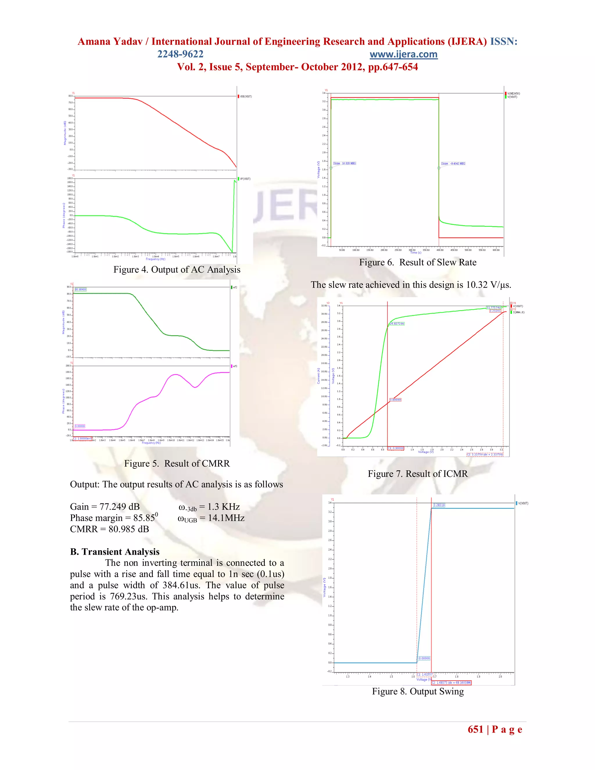
The document details the design and analysis of a two-stage CMOS operational amplifier, highlighting the impact of scaling and aspect ratios on its performance. It describes the methodologies used for optimization in terms of gain, bandwidth, and phase margin, with simulation results indicating a gain of 77.25 dB and a unity gain frequency of 14 MHz. The study emphasizes the challenges in balancing multiple performance parameters as technology evolves and transistor sizes shrink.