Download to read offline

![Kakkeri Roopa et al., International Journal of Emerging Technologies in Computational and Applied Sciences, 9(3), June-August, 2014, pp. 300-
304
IJETCAS 14- 641; © 2014, IJETCAS All Rights Reserved Page 304
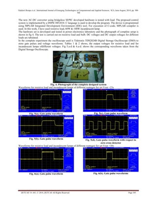
Fig. 6(c). Gate pulse waveform
Fig. 6(d). Gate pulse waveform with respect to zero cross detector
VI. Conclusion
A new AC-DC converter using bridgeless SEPIC has been proposed and verified by experimental works.It is showed that the proposed circuit is capable to achieve high power factor under universal input voltage condition. The capability to reshape the input current is inherent when the circuit is operated in DCM. The main features of the proposed converters include high efficiency, low voltage stress on the semiconductor devices & simplicity of design. This circuit would be most suitable to be used as a switch mode power supply application for low power equipments especially those requiring high quality input power.
In the proposed scheme, DSPIC30F2010 controller is used to produce signals. Experimental circuit of this converter is developed with universal input voltage capability for 20-30V DC output voltage and the developed hardware setup is tested on a resistive load and incandescent lamp(60w,100w) in power electronics laboratory. From the experimental setup and results chapter it is clear that the developed hardware satisfactory converts AC-DC,& can be used in switch mode power supply, equipments which require high quality input power, LED lightning DC motor etc.
VII. Future Scope
This paper has explored some good ideas and suitable solutions, but further investigation is necessary either for telecom and computer server applications or in related field of power management, which are suggested as follows:
1.Dynamic response in low power applications,
2.Design of PFC converter at very high switching frequency,
3.Unbalanced input voltage in modular approach.
Appendix
The following defines the nomenclature and system parameters used in this paper :
Loads: 60W,100W incandescent lamps
Inverter parameters :
Vin :lnput voltage 230V
Cb1,Cb2,Co capacitors
S1,S2MOSFETs
References
[1] D.M. Mitchell, "AC-DC Converter having an improved power factor",U.S. Patent 4,412,277, Oct. 25, 1983.
[2] D. Tollik and A. Pietkiewicz, “Comparative analysis of 1-phase active power factor correction topologies,” in Proc. Int. Telecommunication Energy Conf., Oct. 1992, pp. 517–523.
[3] A. F. Souza and I. Barbi, “High power factor rectier with reduced conduction and commutation losses,” in Proc. Int. Telecommunication Energy Conf., Jun. 1999, pp. 8.1.1–8.1.5
[4] J. Liu, W. Chen, J. Zhang, D. Xu, and F. C. Lee, “Evaluation of power losses in different CCM mode single-phase boost PFC converters via simulation tool,” in Rec. IEEE Industry Applications Conf., Sep. 2001, pp. 2455–2459.
[5] Huber, Laszlo; Jang, Yungtaek; Jovanovic, Milan M.,"Performance Evaluation of Bridgeless PFC Boost Rectifiers" IEEE Transactions on Power Electronics, vol. 23, no 3, pp.1381-1390, May 2008.](https://image.slidesharecdn.com/ijetcas14-641-140911000535-phpapp02/85/Ijetcas14-641-5-320.jpg)

The document presents a new bridgeless single-phase AC-DC converter based on a single-ended primary inductance converter (SEPIC) topology. The proposed rectifier utilizes a bidirectional switch and two fast diodes. It has less conduction losses compared to existing power factor correction rectifiers due to fewer components conducting during each switching cycle. Experimental results show the converter can achieve a high power factor under universal input voltage conditions and provide regulated output voltage for resistive and incandescent lamp loads. Future work may include further optimizing the design for applications requiring high power quality input power.