This document presents a design for a two-channel analog front end (AFE) tailored for ECG signal acquisition, emphasizing low power consumption and high impedance to enhance biomedical electrical signal recording. The AFE incorporates a continuous time Σ-Δ modulator and features programmable gain and low input referred noise, achieving a signal-to-noise ratio (SNR) of 63 dB and a power consumption of 11 mW, simulated in a 0.18 μm CMOS process. The architecture proposes integrating low-noise amplifiers and noise reduction techniques suitable for wearable healthcare applications.
![International Journal of Electrical and Computer Engineering (IJECE)
Vol.8, No.6, December2018, pp. 5041~5049
ISSN: 2088-8708, DOI: 10.11591/ijece.v8i6.pp5041-5049 5041
Journal homepage: http://iaescore.com/journals/index.php/IJECE
A Two Channel Analog Front end Design AFE Design with
Continuous Time ∑-∆ Modulator for ECG Signal
Mohammed Abdul Raheem1
, K Manjunathachari2
1
Department of Electronics and Communication Engineering, Muffakham Jah College of Engineering and Technology,
India
2
Department of Electronics and Communication Engineering, GITAM University, India
Article Info ABSTRACT
Article history:
Received Mar 8, 2018
Revised Jul 23, 2018
Accepted Sep 2, 2018
In this context, the AFE with 2-channels is described, which has high
impedance for low power application of bio-medical electrical activity. The
challenge in obtaining accurate recordings of biomedical signals such as
EEG/ECG to study the human body in research work. This paper is to
propose Multi-Vt in AFE circuit design cascaded with CT modulator. The
new architecture is anticipated with two dissimilar input signals filtered from
2-channel to one modulator. In this methodology, the amplifier is low
powered multi-VT Analog Front-End which consumes less power by
applying dual threshold voltage. Type -I category 2 channel signals of the
first mode: 50 and 150 Hz amplified from AFE are given to 2nd CT sigma-
delta ADC. Depict the SNR and SNDR as 63dB and 60dB respectively,
consuming the power of 11mW. The design was simulated in a 0.18 um
standard UMC CMOS process at 1.8V supply. The AFE measured frequency
response from 50 Hz to 360 Hz, depict the SNR and SNDR as 63dB and
60dB respectively, consuming the power of 11mW. The design was
simulated in 0.18 m standard UMC CMOS process at 1.8V supply. The AFE
measured frequency response from 50 Hz to 360 Hz, programmable gains
from 52.6 dB to 72 dB, input referred noise of 3.5 µV in the amplifier
bandwidth, NEF of 3.
Keyword:
Analog Front End
Continuous Time (CT)
Discrete Time (DT)
Sigma Delta Modulator
Signal Noise Ratio (SNR)
SNDR
Copyright © 2018Institute of Advanced Engineering and Science.
All rights reserved.
Corresponding Author:
M.A. Raheem,
Department of Electronics and Communication Engineering,
MJCET, Osmania University, Hyderabad, India.
Email: abdulraheem.mj@gmail.com
1. INTRODUCTION
ADVANCES in Complementary MOSFET technologies and low powered integrated circuits have
stimulated considerable interests in wearable gadgets, anoccurrence which can potentially transfigure the
healthcare devices. Sensor interface is the main part in the wearable gadgets, design of which should meet
many uncompromising requirements both in digital block and in analog block. In designing AFE circuits, the
corporal signals' nature is of much concern. The amplitude of these signals ranges from volts to mV and the
frequencies vary from DC to a few kilo Hz, as described in figure 1 [1]. The signals, the AFE should possess
lowest input referred noise, reconfigurable bandwidth, and programmable gain to accommodate the weak
signals and giant dynamic range. Furthermore, the skin-electrode interface instigates a high DC potential in
an input signal that should be minimized by high pass filtration, cutting-off frequencies below 1Hz. While,
such a high-pass filter with external capacitors and resistors can be easily implemented [2], it is further cost-
effective to integrate the filter on-chip. Switched-capacitor [3] are two possible approaches that could give
good trade-offs between performance, power, and area as demonstrated in [4], [5]. It is noteworthy that an
approach of pseudo-resistor not only diminishes the area but also ease reconfigurable design of band-pass
filters [6]-[9]. A very high variation of resistances could be the drawback in existing pseudo-resistors which](https://image.slidesharecdn.com/v2823jul188mar12205-21042-3-ed-201127063811/75/A-Two-Channel-Analog-Front-end-Design-AFE-Design-with-Continuous-Time-Modulator-for-ECG-Signal-1-2048.jpg)
![ ISSN:2088-8708
Int J Elec & Comp Eng, Vol. 8, No. 6, December 2018 : 5041 - 5049
5042
are tunable under negative and positive biased conditions. While working on low-voltage, it leads to a critical
DC. In this, recognizing the programmable BE with reconfiguring amplifier the switch in four modes.
Figure 1. Voltage and frequency ranges of familiar physiological signals
Table 1. Medical Characteristics of the Familiar Physiology
Parameter Signal Frequency Standard Sensor
Electroretinography (ERG) DC ~ 50 Hz Contact electrode
Electroencephalography (EEG) DC ~ 150 Hz Scalp electrode
Electrocardiography (ECG) 0.01 Hz ~ 250 Hz Skin electrode
Electroneurography (ENG) 250 Hz ~ 5000 Hz Surface/needle
electrode
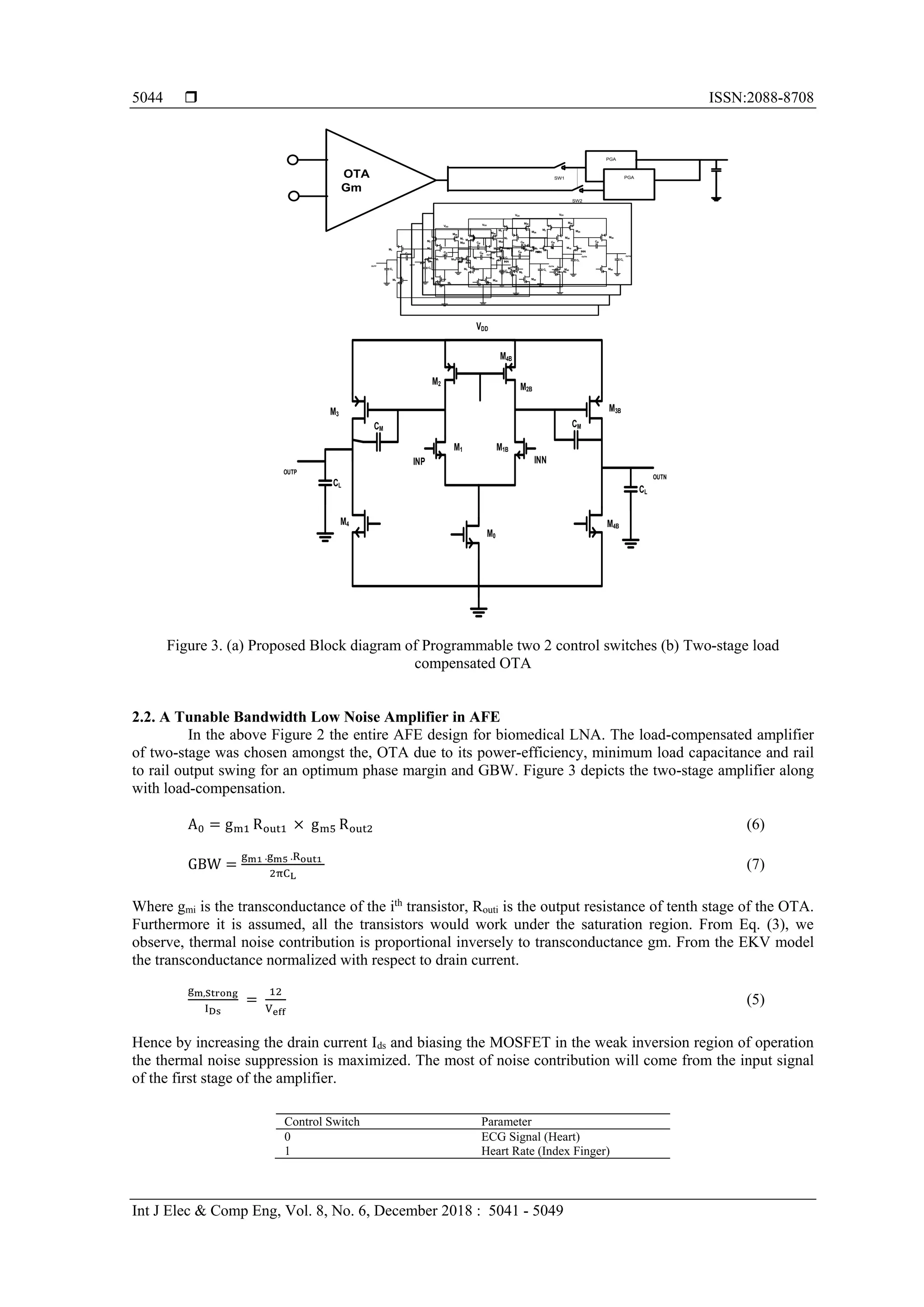
This paper is sectioned as described hereafter. Section-II depicts a Proposed System level
architecture of AFE with Programmable Procedure. An AFE with sigma-delta modulator is delineated in
Section III. Results from simulation and related thoughts are furnished in Section IV. Hence, the conclusions
are derived under Section V.
2. THE PROPOSED ARCHITECTURE 2- CHANNEL AFE FOR ECG SIGNAL MODULATOR
This paper addresses a chip that comprises a low noise (TB-FEA), a programmable gain amplifier
(PGA) and a 10-bitƩΔ (SDM-ADC). The overall gain is programmed through the flip-over-capacitor
feedback and proposed reconfiguring in the PGA. This allows the chip to offer FOUR operational modes,
ERG, EEG, ECG, and ENG.
The microsystem for acquisition of bio-potential is as shown in figure 2. Bio-signals are amplified
by AFE circuits and then they are converted into digital codes by ADCs [3]. In addition, analog multiplexers
with large output current are designed to select the corresponding signals to ADCs. A trade-off in the
microsystem exists between power and the area. The ratio between count of AFEs and ADCs affects the
inclusivefunctioning.](https://image.slidesharecdn.com/v2823jul188mar12205-21042-3-ed-201127063811/75/A-Two-Channel-Analog-Front-end-Design-AFE-Design-with-Continuous-Time-Modulator-for-ECG-Signal-2-2048.jpg)
![Int J Elec& Comp Eng ISSN: 2088-8708
A Two Channel Analog Front End Design AFE Design with Continuous Time ∑-∆ … (M.A. Raheem)
5043
+
_
+
_
RBIAS
RBIAS
LPF
LPF
ANALOG FRONT END
AmplifierECG
HEART
RATE
INSTRUMENTATION
AMPLIFIERS
Second order
∑-∆ ADC
Amplifier
ANALOGMULTIPLEXER
ON
LPF1
PGA
CLOCK GENERATOR
ANALOGMULTIPLEXER
SAMPLED
CLOCK
SYSTEM
CLOCK
PROBE 1
PROBE 2
OUTPUT
BIASING CIRCUITS
Control
Switch BW
& Gain
CT ADC –
2nd
Order
Front End
Differential
Amplifier
Figure 2. Proposed architecture of 2 channel
2.1. Noise Contribution at AFE design
The Flicker Noise 1/f reduction always remains a challenge in the bio-signal acquisition. This
problem cannot be avoided completely 1/f noise exist in all the devices of MOSFET due to their surface
conduction mechanism. For a MOS working in saturation region the total flicker noise power spectrum could
be calculated as
gm = √2. meff. Cox.
W
L
. Ids (1)
if
2
= al.
q.mf. (Vgs−Vt).Ids
L2.f
(2)
The spectral density for a MOSFET is given from [9] as:
vf
2
= 4kT
2
3
1
gm
+
Kf
WLCoxf
(3)
Thermal Flicker](https://image.slidesharecdn.com/v2823jul188mar12205-21042-3-ed-201127063811/75/A-Two-Channel-Analog-Front-end-Design-AFE-Design-with-Continuous-Time-Modulator-for-ECG-Signal-3-2048.jpg)
![Int J Elec& Comp Eng ISSN: 2088-8708
A Two Channel Analog Front End Design AFE Design with Continuous Time ∑-∆ … (M.A. Raheem)
5047
NEF = Vrms, in√
2 I total
πVt.4kT.Bandwidth
(8)
where Vrmsin is the input-referred noise, is the total current, is the thermal voltage, and BWis the
bandwidth of the AFE with chopping technique.Usually AFE circuits attain a NEF of 2.5 to 10. The complete
layout design with IO pad of the 2 channel AFE with modulator is shown in Figure 8. The Area occupied by
the filter is 209.41 µm × 80.21 µm = 0.0167 mm2
.
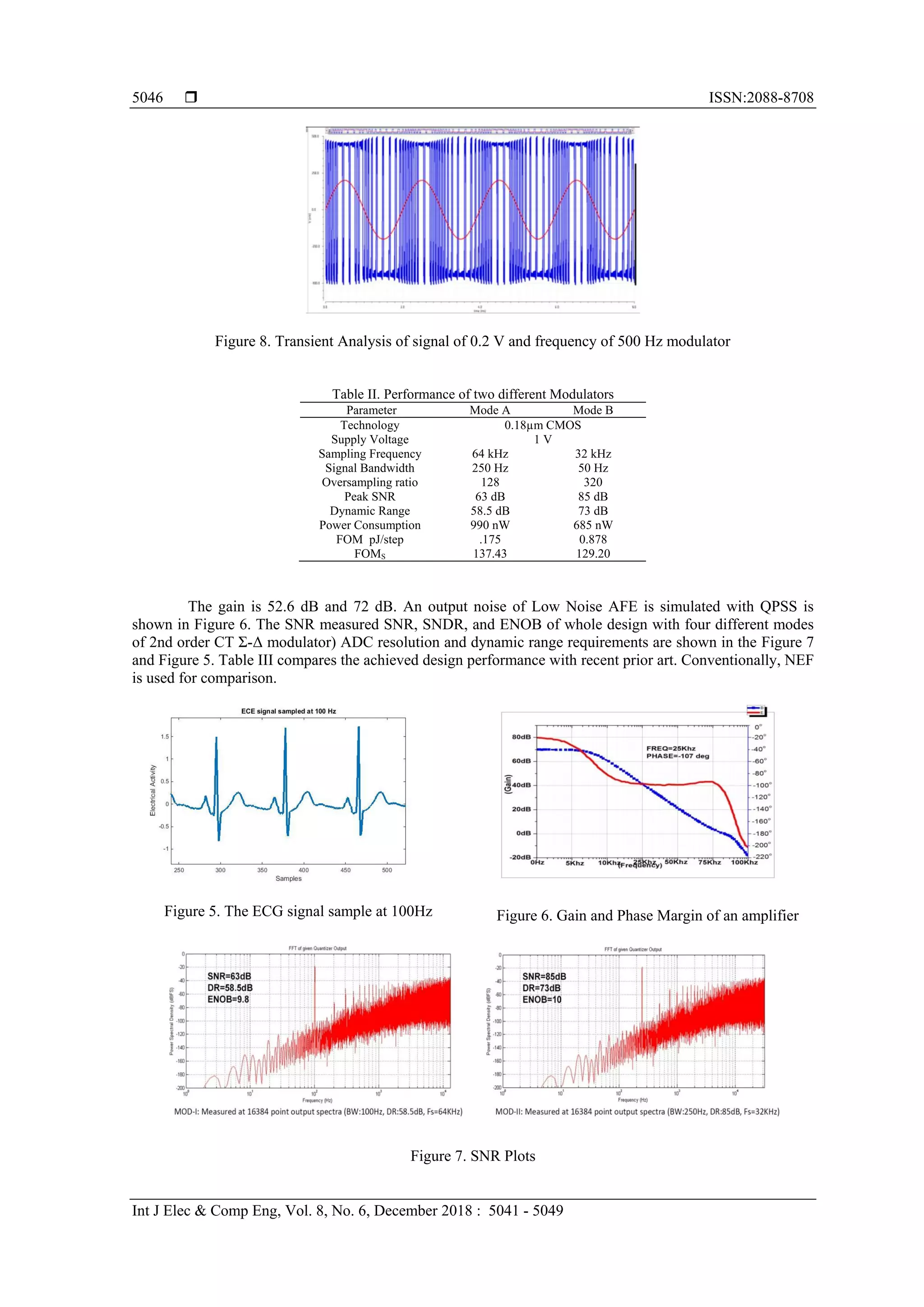
Figure 8. Final Layout of AFE with Dual Sigma-Delta Modulator
Power role of the different blocks is shown in Figure 9. As seen in Figure, more than half of the
power budget is dedicated to the different mode of 2nd order CT Ʃ-Δ modulator. The chopping switch and
clock generator are consumed more power when compared to amplifier due to noise considerations.
Figure 9. Power Consumption and distribution in Pie chart of whole design
Table III. Comparison of PRIOR ART
Parameter [7] [8] [9] [11] This Work
Tech.(μm) 0.5 0.18 0.8 0.13 0.18
Supply (V) 2.8 1.5 1.8 1.2 1
Bias (nA) 743 5000 1050 580a
/902b
500
Gain (dB) 40.9 40.8 41-50.5 40-83 52.8-72
Input Ref.Noise(µVrms) 1.66 1.27 0.98 2.06 3.5
HPF (Hz) 0.4 0.5 0.05- 0.4 0.17 0.1
LPF (KHz) 0.045-5.3 0.1-0.4 0.120 0.34-7.5 7.0
NEF 3.21 6.1 4.6 – 5.4 3.28a
/4.1b
3.04
Progamm
able
amplifier
with
switches,
36%
Low Noise
Amplifier
7%
output
stage; 4%
Two
Modes
Modulato
r, 544%
CMFB; 9%](https://image.slidesharecdn.com/v2823jul188mar12205-21042-3-ed-201127063811/75/A-Two-Channel-Analog-Front-end-Design-AFE-Design-with-Continuous-Time-Modulator-for-ECG-Signal-7-2048.jpg)
![ ISSN:2088-8708
Int J Elec & Comp Eng, Vol. 8, No. 6, December 2018 : 5041 - 5049
5048
4. CONCLUSION
In this paper, a 2-channel ECG amplifier with appropriate features for dry and non-contact
biopotential applications is presented. Unable to compare the complete design with other design this paper
proposed the architectural system level design which is suitable for biomedical application targeted to ECG
for 10 mV to 100 mV. Especially, in this paper the multi-VT concept is implemented in the circuit level
which reduces the power consumption and the gain achieved by amplifier 52.9dB and 72 dB with an NEF
3.0, noise performance is satisfactory. Furthermore, another important approach the two different 2nd order
CT Ʃ-Δ modulator to improve the performance.
ACKNOWLEDGEMENTS
The authors would like to express their great appreciations and gratitude to Muffakham Jah College
of Engineering and Technology for providing research facilities, technical support, and research
environment.
REFERENCES
[1] Y.M. Chi, Y.T. Wang, Y. Wang, Ch. Maier, T.P. Jung, and G. Cauwenberghs, “Dry and non-contact EEG sensors
for mobile brain-computer interfaces”, IEEE Transactions on Neural Systems and Rehabilitation Engineering, vol.
20, no. 2, March 2012
[2] M. Steffen, A. Aleksandrowicz, and S. Leonhardt, “Mobile noncontact monitoring of heart and lung activity”, IEEE
Transactionson Biomedical Circuits and Systems, vol. 1, no. 4, pp. 250-257, Dec. 2007.
[3] J. Kranjec, S. Beguš, J. Drnovšek, and G. Geršak, “Novel methods for non-contact heart rate measurement: A
feasibility study”, IEEE Transactions on Instrumentation and Measurement, vol. 63, no. 4, April 2014
[4] Y.G. Lim, K.K. Kim, and K.S. Park, "ECG recording on a bed during sleep without direct skin-contact", IEEE
Transactions on Biomedical Engineering, vol. 54, pp. 718-725, 2007.
[5] S. Leonhardt, and A. Aleksandrowicz, “Non-contact ECG monitoring for automotive application”, 5th
International Summer Schooland Symposium on Medical Devices and Biosensors, ISSS-MDBS, June 2008, pp. 183-
185.
[6] X.X. Chen, Y. Lv, R.R. Zhen Fang, Sh. H. Xia, and H. Li, Li. Tian,“A wireless non-contact ECG detection system
based on capacitive coupling”, IEEE 14th International Conference on e-Health Network.
[7] W. Wattanapanitch, et al., “An energy-efficient micropower neural recording amplifier”, IEEE Trans. on
Biomedical Circuits and Systems, vol. 1, pp. 136-147, June 2007.
[8] S. Kao, et al., “A 1.5V 7.5µW programmable gain amplifier for multiple biomedical signal acquisition”, IEEE
Biomedical Circuits and Systems Conference, 2009, pp. 73-76.
[9] T. Denison, et al., “A 2µW 100nV/rt Hz chopper-stabilized instrumentation amplifier for chronic measurement of
neural field potentials”, IEEE J. of Solid-State Circuits, vol. 42, pp. 2934-2945, Dec. 2007.
[10] T. Yoshida,et al., “A high-linearity low-noise amplifier with variable bandwidth for neural recording systems”,
Japanese J. of Applied Physics, vol. 50, pp. 1-4, April 2011.
[11] Christopher J. Mandic, DebashishGangopadhyay and David J. Alls, “ A 1.1µW 2.1µVRMS Input Noise Chopper-
stabilized Amplifier for Bio-medical Applications”, Circuits and Systems (ISCAS), 2012 IEEE International
Symposium on 20-23 May 2012, Seoul, South Korea
[12] Y.M. Chi, T.P. Jung, and G. Cauwenberghs, “Dry-contact and noncontactbiopotential electrodes: methodological
review”, IEEE Reviews in Biomedical Engineering, vol. 3, 2010
[13] Y. Ch. Chen, B. Sh. Lin, and J. Sh. Pan, “Novel non-contact dry electrode withanadaptive mechanical design for
measuring EEG in ahairy site”, IEEE Transactions on Instrumentation and Measurement, vol. 64, no. 12, pp. 3361
– 3368, Dec. 2015.
[14] Y.M. Chi, Ch. Maier, and G. Cauwenberghs, “Ultra-high input impedance, low noise integrated amplifier for non-
contact biopotential sensing”, IEEE Journal on Emerging and Selected Topics in Circuitsand Systems, vol. 1, no. 4,
Dec. 2011.
[15] F. Rummens, S. Renaud and N. Lewis, “CMOS differential neural amplifier with high input impedance”, The 13th
IEEE International NEW Circuits and Systems (NEWCAS) conference, June 2015, pp. 1-4.
[16] P. Monsurro, S. Pennisi, G. Scotti, and A. Trifiletti, “Inverting closed loop amplifier architecture with reduced gain
error and high input impedance”, IEEE International Symposium on Circuits and Systems (ISCAS), May 2006.
[17] N. Verma, A. Shoeb, J. Bohorquez, J. Dawson, J. Guttag, and A. P.Chandrakasan, “A micro-power EEG
acquisition SoC with integrated feature extraction processor for a chronic seizure detection system”, IEEE J. Solid-
State Circuits, vol. 45, no. 4, pp. 804–816, Apr. 2010.
[18] L. Fay, V. Misra, and R. Sarpeshkar, “A micropower electrocardiogram amplifier”, IEEE Transaction Biomedical
Circuitand System, vol. 3, no. 5, Oct. 2009.
[19] S. Ha et al., “Integrated circuits and electrode interfaces for Noninvasive physiological monitoring”, IEEE
Transactions on Biomedical Engineering, vol. 61, no. 5, pp. 1522-1537, May 2014.
[20] H.F. Achigui, M. Sawan, C.J.B. Fayomi, “A 1 V Low Power, Low Noise DTMOS based NIRS Front-End
Receiver”, in Proc. WMSCI, Jully 2005.](https://image.slidesharecdn.com/v2823jul188mar12205-21042-3-ed-201127063811/75/A-Two-Channel-Analog-Front-end-Design-AFE-Design-with-Continuous-Time-Modulator-for-ECG-Signal-8-2048.jpg)
![Int J Elec& Comp Eng ISSN: 2088-8708
A Two Channel Analog Front End Design AFE Design with Continuous Time ∑-∆ … (M.A. Raheem)
5049
[21] Qu Ruoyuan, Li Tong, Li Xiao, XuMinglu, Chen Yueyang, Wang Xinghua, “Wireless Neural Acquisition System
Design”, 2013 35th
Annual International Conference of the IEEE Engineering in Medicine and Biology Society.
[22] A. FazliYeknami and A. Alvandpour, “A 0.5-V 250-NW 65-dB SNDR Passive ΔΣ Modulator for Medical Implant
Devices”, in Proc. IEEE InternationalSym.Circuits and Systems, May 2013, pp. 2010-2013.
[23] M.A. Raheem, K. Manjunathaachari, and Arifuddinsohel. “A Design of 2nd
Order DT Sigma-Delta Modulator for
Medical Implants”, in Proc. IEEE PrimeAsia, Dec 2015,978-1-5090-0136-1/15/$31.00 ©2015 IEEE
[24] M.A. Raheem, K. Manjunathaachari, “presented as paper presentation IEEE paper “A Logarithmic DWA based
Discrete Time MultibitSigma-DeltaModulator”, IEEE sponsored conference INBUSH ERA 2015. ISBN:978-1-
4799-8432-9 at Amity University Greater Noida Feb25 -27 2015”
[25] M.A. Raheem, Mohammed Arifuddin Sohel and Maliha Naaz “Design of Discrete-Time Notch Filter for
Biomedical Applications”, in Conference Proc. IEEE Device of Integrated Circuits DevIC 2017 10.1109/DEVIC
2017.8073997
[26] Maizan Muhamad, NorhayatiSoin and Harikrishna Ramiah “Design of Low power Low Noise Amplifier using
Gm- boosted Technique”, in Indonesian Journal of Electrical Engineering and Computer Science ISSN: 2502-
4752, DOI: 10.11591/ijeecs. v9. i3. pp685-689
[27] M.A. Raheem, Mohammed Arifuddin Sohel and Maliha Naaz “Design of Discrete-Time Notch Filter for
Biomedical Applications”, in International Journal of Innovative Research in Electrical, Electronics,
Instrumentation, and control Engineering, Vol 4 issue 12, December 2016
[28] Ahmed Al-Hashimi, Anis Nurashikin Nordin*, Amelia Wong Azman, “Design of a Reconfigurable, Modular and
Multi-Channel Bioimpedance Spectroscopy System”, in Indonesian Journal of Electrical Engineering and
Computer Science, DOI: 10.11591/ijeecs. v8. i2. pp428-440
[29] M.A. Raheem, Mohammed Arifuddin Sohel and Maliha Naaz, “Quad Mode of Sixteen-Channel Chopper AFE
Design and Cascaded with Continuous Time ∑-∆ Modulator for Electroencephalogy Monitory System”, in
International Journal of Simulation, Systems, Science and Technology ISSN 1473-8031Research in Electrical,
Electronics, Instrumentation and control Engineering, Vol 8 Number 3, September 2017
[30] A. AAmin, M.S. Islam, M.A. Masud, M.N.H. Khan, “Design and Performance Analysis of 1.8 GHz Low Noise
Amplifier for Wireless Receiver Application”, in Indonesian Journal of Electrical Engineering and Computer
Science DOI: 10.11591/ijeecs. v6. i3. pp656-662
BIOGRAPHIES OF AUTHORS
Abdul Raheem is a research scholar from Hyderabad, Telangana, India. He has completed id
Bachelors in Engineering in 2005, and Masters in VLSI System Design from GRIET, JNTU
Hyderabad, currently doing P.hD at Gitam University As a research Scholar in Micro-electronics
in Analog & amplifiers; Mixed Signal, Hyderabad, India. His Current research mainly focuses
on CMOS Analog- Mixed signal Integrated Circuits. His current focus to design Low power
architectures for biomedical application. His ongoing work design are focus to Analog Front
Design, low power design of Sigma Delta Modulator and bandgap reference circuits. He is
expert in IC EDA tools interfacing with Specification to GDSII. He has presented a papers 21
National and International IEEE Conference. He also received best paper award in IEEE
Conference of Post Graduate Research in Micro-Electronics ASIA (PRIME ASIA 2015)
K Manjuanthachari is currently a professor and Head of the Electronic & Communication
Engineering Department at Gitam University Hyderabad Telangana, and his research in Signal
Processing and Image Processing, MPEG, with Interfacing with FPGA, He has enormous
experience in teaching and industry, he is guiding the 12 research scholar at Gitam University.
He has 50 plus publications in National and International Journal /Conferences.](https://image.slidesharecdn.com/v2823jul188mar12205-21042-3-ed-201127063811/75/A-Two-Channel-Analog-Front-end-Design-AFE-Design-with-Continuous-Time-Modulator-for-ECG-Signal-9-2048.jpg)