Low-power 1-bit full adder techniques review
•
1 like•250 views

In this work a comparison and study of different low power 1-bit full adder techniques at deep submicron technologies is carried out. The study concentrates in the crucial factors which determine the applicability of the design for particular applications. The comparison of different adders has been carried out on the basis of these parameters i.e. delay, power consumption, output swing, PDP etc. The comparison is carried out between designs with low device count. On the basis of comparison a conclusion has been drawn in which the shortcomings of present designs have been discussed with future possibilities of improvement. The designs compared are TGA, SERF and modified SERF.
![A Review of Low-Energy 1-Bit Full Adder Techniques for Power Deprived Applications
(IJSRD/Vol. 2/Issue 09/2014/050)
All rights reserved by www.ijsrd.com 219
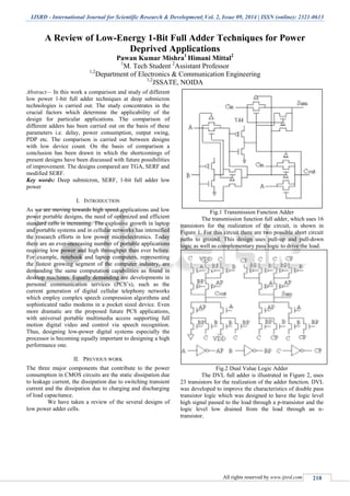
Fig. 3 14T Full Adder Cell
The fourteen transistor full-adder, as the name
implies, uses 14 transistors to realize the adder function-
Figure 3. To date this is the most area efficient design. The
14T full adder cell, like the transmission function full adder
cell, implements the complementary pass logic to drive the
load.
A. Serf Adder Cell
Fig.4 Conventional SERF ADDER
SERF design implies only 10 transistors to
implement a full adder cell. This circuit operates well at
higher supply voltages, but if the supply voltage is scaled to
voltages lower than 0.3V, this circuit fails to work. As it can
be seen, the SERF adder is confronted with serious
problems especially at lower supply voltages. Assume that
one of the two input vectors ABCin=“110” and “111” are
applied. As seen from Figure.4, when A=1 and B=1, the F
node voltage is Vdd-Vth. Now if Cin=0 then Cout will be
equal to Vdd-2Vth and the Sum signal isgoing to zero
driven by a MOS transistor with its gate connected to Vdd-
Vth. When Cin=1, Cout is connected to VDD (may be
lower) and the SUM signal will go to Vdd-Vth. Another
problem with this design is when the floating node is
connected to 0 (A=0, B=1 or A=1,B=0).When Cin is “1”,
Cout is charged to Vdd, but when Cin=0, Cout must be
discharged to ground using a PMOS pass transistor that
cannot fully discharge the output. In this case, Cout is
discharged toVtp which is higher than Vtn. This problem is
intensified if the circuit works at sub threshold voltage. If A
is at logic “1”, some current leaks to the Cout node which
makes Cout to increase even more than Vtpin some cases
depending on the sizing of the pass transistors. In thiscase
the Sum value is dependent on the Cin state, for instance, if
Cin is “1”, the Sum output is going to Vdd-Vth which is a
problem in sub threshold region.
B. Modified Serf Adder
Fig.5 Modified SERF ADDER CELL
For the modifications in conventional SERF adder
cell for different inputs, we add an extra circuit to the SERF
adder as shown in Figure 5. By adding this circuit to the
SERF, the F node voltage for input vectors ABCin=(“110”,
“111”), is connected to VDD, which increases the output by
Vth, so we can scale the supply voltage to Vtn+Vtp that is
estimated to be lower than 0.3V instead of 0.45V for SERF
full adder.
III. PROPOSED WORK
There are 2 possible improvements which can be applied
separately to SERF in order to achieve different
performance goals according to applications. The proposed
designs are:
Full swing design (FS-SERF)
High speed design (HS-SERF)
Both designs can work at Vdd as low as 0.3V.
IV. CONCLUSION
In this paper we have surveyed the various full adder cells
i.e. TGA, SERF and Modified SERF along with their basic
structures. The SERF is modifies with the introduction of an
extra circuit to the conventional SERF and as a result the
power consumption of the SERF adder cell has reduced.
Further, the modified circuit can be improved by adding two
proposed designs i.e. Full swing design and high speed
design which would work at 0.3V power supply and
performance will be enhanced accordingly.
REFERENCES
[1] N. Weste and K. Eshraghian, “Principles of CMOS
digital design” Reading, MA: Addison-Wesley, pp.
304–307.](data:image/gif;base64,R0lGODlhAQABAIAAAAAAAP///yH5BAEAAAAALAAAAAABAAEAAAIBRAA7)
Recommended
Recommended
More Related Content
What's hot
What's hot (19)
Similar to Low-power 1-bit full adder techniques review
Similar to Low-power 1-bit full adder techniques review (20)
More from ijsrd.com
More from ijsrd.com (20)
Recently uploaded
Recently uploaded (20)
Low-power 1-bit full adder techniques review
- 1. IJSRD - International Journal for Scientific Research & Development| Vol. 2, Issue 09, 2014 | ISSN (online): 2321-0613 All rights reserved by www.ijsrd.com 218 A Review of Low-Energy 1-Bit Full Adder Techniques for Power Deprived Applications Pawan Kumar Mishra1 Himani Mittal2 1 M. Tech Student 2 Assistant Professor 1,2 Department of Electronics & Communication Engineering 1,2 JSSATE, NOIDA Abstract— In this work a comparison and study of different low power 1-bit full adder techniques at deep submicron technologies is carried out. The study concentrates in the crucial factors which determine the applicability of the design for particular applications. The comparison of different adders has been carried out on the basis of these parameters i.e. delay, power consumption, output swing, PDP etc. The comparison is carried out between designs with low device count. On the basis of comparison a conclusion has been drawn in which the shortcomings of present designs have been discussed with future possibilities of improvement. The designs compared are TGA, SERF and modified SERF. Key words: Deep submicron, SERF, 1-bit full adder low power I. INTRODUCTION As we are moving towards high speed applications and low power portable designs, the need of optimized and efficient standard cells is increasing. The explosive growth in laptop and portable systems and in cellular networks has intensified the research efforts in low power microelectronics. Today there are an ever-increasing number of portable applications requiring low power and high throughput than ever before. For example, notebook and laptop computers, representing the fastest growing segment of the computer industry, are demanding the same computation capabilities as found in desktop machines. Equally demanding are developments in personal communication services (PCS’s), such as the current generation of digital cellular telephony networks which employ complex speech compression algorithms and sophisticated radio modems in a pocket sized device. Even more dramatic are the proposed future PCS applications, with universal portable multimedia access supporting full motion digital video and control via speech recognition. Thus, designing low-power digital systems especially the processor is becoming equally important to designing a high performance one. II. PREVIOUS WORK The three major components that contribute to the power consumption in CMOS circuits are the static dissipation due to leakage current, the dissipation due to switching transient current and the dissipation due to charging and discharging of load capacitance. We have taken a review of the several designs of low power adder cells. Fig.1 Transmission Function Adder The transmission function full adder, which uses 16 transistors for the realization of the circuit, is shown in Figure 1. For this circuit there are two possible short circuit paths to ground. This design uses pull-up and pull-down logic as well as complementary pass logic to drive the load. Fig.2 Dual Value Logic Adder The DVL full adder is illustrated in Figure 2, uses 23 transistors for the realization of the adder function. DVL was developed to improve the characteristics of double pass transistor logic which was designed to have the logic level high signal passed to the load through a p-transistor and the logic level low drained from the load through an n- transistor.
- 2. A Review of Low-Energy 1-Bit Full Adder Techniques for Power Deprived Applications (IJSRD/Vol. 2/Issue 09/2014/050) All rights reserved by www.ijsrd.com 219 Fig. 3 14T Full Adder Cell The fourteen transistor full-adder, as the name implies, uses 14 transistors to realize the adder function- Figure 3. To date this is the most area efficient design. The 14T full adder cell, like the transmission function full adder cell, implements the complementary pass logic to drive the load. A. Serf Adder Cell Fig.4 Conventional SERF ADDER SERF design implies only 10 transistors to implement a full adder cell. This circuit operates well at higher supply voltages, but if the supply voltage is scaled to voltages lower than 0.3V, this circuit fails to work. As it can be seen, the SERF adder is confronted with serious problems especially at lower supply voltages. Assume that one of the two input vectors ABCin=“110” and “111” are applied. As seen from Figure.4, when A=1 and B=1, the F node voltage is Vdd-Vth. Now if Cin=0 then Cout will be equal to Vdd-2Vth and the Sum signal isgoing to zero driven by a MOS transistor with its gate connected to Vdd- Vth. When Cin=1, Cout is connected to VDD (may be lower) and the SUM signal will go to Vdd-Vth. Another problem with this design is when the floating node is connected to 0 (A=0, B=1 or A=1,B=0).When Cin is “1”, Cout is charged to Vdd, but when Cin=0, Cout must be discharged to ground using a PMOS pass transistor that cannot fully discharge the output. In this case, Cout is discharged toVtp which is higher than Vtn. This problem is intensified if the circuit works at sub threshold voltage. If A is at logic “1”, some current leaks to the Cout node which makes Cout to increase even more than Vtpin some cases depending on the sizing of the pass transistors. In thiscase the Sum value is dependent on the Cin state, for instance, if Cin is “1”, the Sum output is going to Vdd-Vth which is a problem in sub threshold region. B. Modified Serf Adder Fig.5 Modified SERF ADDER CELL For the modifications in conventional SERF adder cell for different inputs, we add an extra circuit to the SERF adder as shown in Figure 5. By adding this circuit to the SERF, the F node voltage for input vectors ABCin=(“110”, “111”), is connected to VDD, which increases the output by Vth, so we can scale the supply voltage to Vtn+Vtp that is estimated to be lower than 0.3V instead of 0.45V for SERF full adder. III. PROPOSED WORK There are 2 possible improvements which can be applied separately to SERF in order to achieve different performance goals according to applications. The proposed designs are: Full swing design (FS-SERF) High speed design (HS-SERF) Both designs can work at Vdd as low as 0.3V. IV. CONCLUSION In this paper we have surveyed the various full adder cells i.e. TGA, SERF and Modified SERF along with their basic structures. The SERF is modifies with the introduction of an extra circuit to the conventional SERF and as a result the power consumption of the SERF adder cell has reduced. Further, the modified circuit can be improved by adding two proposed designs i.e. Full swing design and high speed design which would work at 0.3V power supply and performance will be enhanced accordingly. REFERENCES [1] N. Weste and K. Eshraghian, “Principles of CMOS digital design” Reading, MA: Addison-Wesley, pp. 304–307.
- 3. A Review of Low-Energy 1-Bit Full Adder Techniques for Power Deprived Applications (IJSRD/Vol. 2/Issue 09/2014/050) All rights reserved by www.ijsrd.com 220 [2] A. P. Chandrakasan, S. Sheng, and R. W. Brodersen, “Low- power CMOS digital design,” IEEE J. Solid-State Circuits, vol. 27, pp. 473– 484,Apr. 1992. D. Radhakrishnan, “Low voltage CMOS full adder cells,” Electronic letters, vol. 35, pp. 1792-1794, 1999. [3] A. P. Chandrakasan and R.W. Brodersen, “Minimizing power consumption in digital CMOS circuits,” Proc. IEEE, Apr. 1995, vol. 83, No. 4, pp. 498–523. [4] W. C. Athas and N. Tzartzanis, “Energy Recovery for Low Power CMOS”, Proc. Of 16th Conference on Advanced Research in VLSI, 1995, pp. 415- 429. [5] Ricardo Gonzalez, Benjamin M. Gordon, and Mark A. Horowitz, “Supply and Threshold Voltage Scaling for Low Power CMOS”, IEEE J. Solid- State Circuits, Vol. 32, No. 8, Aug. 1997, pp. 1210- 1216. [6] Q. Wu, P. Massoud, X. Yu, “Clock-Gating and Its Application to Low Power Design of Sequential Circuits,” Proc. Of the IEEE Custom Integrated CircuitsConference, 1997, pp. 425-435. [7] Gutnik, A. Chandrakasan, “Embedded Power Supply for Low-Power DSP,” IEEE Transactions on VLSI Systems, Dec. 1997, Vol. 12, pp. 425-435. [8] [A. Wang, A. P. Chandrakasan, S. V. Kosonocky, “Optimal Supply and Threshold Scaling for Subthreshold CMOS Circuits”, Proc. Of IEEE Computer Society Annual Symposium on VLSI, 2002, pp. 5-9. [9] R. Shalem, E. John and L. K . John, “A novel low power energy recovery full adder cell”, Proc. Of the IEEE Great Lakes Symposium of VLSI, Feb. 1999, pp. 380-383. [10]Yingtao Jiang, Abdulkarim Al-Sheraidah, Yuke Wang, Edwin Sha, and Jin- Gyun Chung, “A Novel Multiplexer-Based Low-Power Full Adder”, IEEE Transactions on Circuits and Systems II: Express Briefs, July 2004, Vol. 51, No. 7, , PP. 345-348. [11]H. T. Bui, A. K. Al-Sheraidah, and Y. Wang, “Design and analysis of 10- transistor full adders using novel XOR-XNOR gates,” Proc. Of Int. Conf. on Signal Processing (Wold Computer Congress), Beijing, China, Aug. 2000. [12]Y. Jiang, Y. Wang, and J. Wu, “Comprehensive power Evaluation of Full Adders,” Florida Atlantic Univ., BocaRaton, Tech. Rep., 2000.