Downloaded 39 times
![Int. Journal of Electrical & Electronics Engg. Vol. 2, Spl. Issue 1 (2015) e-ISSN: 1694-2310 | p-ISSN: 1694-2426
55 NITTTR, Chandigarh EDIT-2015
Design and Analysis of CMOS Instrumentation
Amplifier
Aayushi Sharma
Chitkara University, Himachal Pradesh,India
Abstract-This paper presents the design and analysis of
CMOS Instrumentation Amplifier in terms of gainas a
performance metric. CMOSInstrumentation Amplifier has
been designed using three Operational Amplifiers. Two basic
op-amps have been used at the input stage and the output
stage have been analysed for three different configurations.
These configurations are: basic op-amp, body bias op-amp
and folded cascode op-amp. A comparison has been drawn
for all the three configurations.Most of the previous work has
been done usingthe same type of op-amp at both the input
and output stages of instrumentation amplifier. To obtain the
desirableGain, focus has been laid upon transistor sizing for
designing. The design models have been implemented using
Cadence Virtuoso Analog Design Suite in 0.18µm CMOS
technology.The simulations have been analysed in detail. A
significant gain improvement has been observed in the circuit
design with body bias and folded cascode as compared to the
basic cascade design.
Keywords- Instrumentation amplifier, Gain, Folded cascode
amplifier, Body Bias
INTRODUCTION
Instrumentation amplifier aims at the amplification of the
desired signal and elimination of the noisy signals or the
common mode signals that affect the original signal
strength. The amplification of very weak amplitude signals
in the order of few mV is a challenging task.With the help
of simple operational amplifiers one is able to strengthen
these weak signals along with the noise amplification.
Instrumentation amplifiers are a kind of the differential
amplifier which consists of the input buffer amplifier so
that the need for the input impedance matching is not
required.Other characteristics like low noise, low dc
offset,high open-loop gain, high common mode rejection
ratio and high input impedance [1].Gain improvement can
be achieved by cascading of stages.Due to the very high
common mode rejection ratio and less power requirement
these instrumentation amplifiers are used in various
applications.
The rest of the paper is organized as follows:Section II
describes the instrumentation amplifier design. Simulation
results are discussed in SectionIII and section IV concludes
the paper.
INSTRUMENTATIONAMPLIFIER DESIGN
The basic cascade instrumentation amplifier has been
designed using three op-amps, two at the input side and
one at the output as shown in fig 1. The input side of all the
three implemented configurations is the same. However, at
the output stage the circuit has been designed and analyzed
for three different configurations.
Fig.1 Instrumentation Amplifier Circuit[2]
Table I shows the value of different resistances considered
for the circuit design. The values of resistances are set such
that to R3=R4=R5=R6 and R1 is very small as compared
to other resistors to achieve high gain. The output voltage
of the instrumentation amplifieris given by
Vout=-( − )*(1+2 / )( / )
TABLE I. Resistance Values
Resistors Resistance Value (Ω)
R1 100
R2, R3 20K
R4, R5, R6 20K
Operational Amplifier 1 and 2 have been designed using
Differential Amplifier connected in non- inverting
configuration followed by CommonSource Amplifier
circuit as shown in fig 2 and 3.
Fig. 2Input Stage of Operational Amplifier
Input Stage
Output Stage
Current
MirrorLoad
Differential Pair](https://image.slidesharecdn.com/id104-150526191342-lva1-app6892/85/Design-and-Analysis-of-CMOS-Instrumentation-Amplifier-1-320.jpg)
![Int. Journal of Electrical & Electronics Engg. Vol. 2, Spl. Issue 1 (2015) e-ISSN: 1694-2310 | p-ISSN: 1694-2426
55 NITTTR, Chandigarh EDIT-2015
Design and Analysis of CMOS Instrumentation
Amplifier
Aayushi Sharma
Chitkara University, Himachal Pradesh,India
Abstract-This paper presents the design and analysis of
CMOS Instrumentation Amplifier in terms of gainas a
performance metric. CMOSInstrumentation Amplifier has
been designed using three Operational Amplifiers. Two basic
op-amps have been used at the input stage and the output
stage have been analysed for three different configurations.
These configurations are: basic op-amp, body bias op-amp
and folded cascode op-amp. A comparison has been drawn
for all the three configurations.Most of the previous work has
been done usingthe same type of op-amp at both the input
and output stages of instrumentation amplifier. To obtain the
desirableGain, focus has been laid upon transistor sizing for
designing. The design models have been implemented using
Cadence Virtuoso Analog Design Suite in 0.18µm CMOS
technology.The simulations have been analysed in detail. A
significant gain improvement has been observed in the circuit
design with body bias and folded cascode as compared to the
basic cascade design.
Keywords- Instrumentation amplifier, Gain, Folded cascode
amplifier, Body Bias
INTRODUCTION
Instrumentation amplifier aims at the amplification of the
desired signal and elimination of the noisy signals or the
common mode signals that affect the original signal
strength. The amplification of very weak amplitude signals
in the order of few mV is a challenging task.With the help
of simple operational amplifiers one is able to strengthen
these weak signals along with the noise amplification.
Instrumentation amplifiers are a kind of the differential
amplifier which consists of the input buffer amplifier so
that the need for the input impedance matching is not
required.Other characteristics like low noise, low dc
offset,high open-loop gain, high common mode rejection
ratio and high input impedance [1].Gain improvement can
be achieved by cascading of stages.Due to the very high
common mode rejection ratio and less power requirement
these instrumentation amplifiers are used in various
applications.
The rest of the paper is organized as follows:Section II
describes the instrumentation amplifier design. Simulation
results are discussed in SectionIII and section IV concludes
the paper.
INSTRUMENTATIONAMPLIFIER DESIGN
The basic cascade instrumentation amplifier has been
designed using three op-amps, two at the input side and
one at the output as shown in fig 1. The input side of all the
three implemented configurations is the same. However, at
the output stage the circuit has been designed and analyzed
for three different configurations.
Fig.1 Instrumentation Amplifier Circuit[2]
Table I shows the value of different resistances considered
for the circuit design. The values of resistances are set such
that to R3=R4=R5=R6 and R1 is very small as compared
to other resistors to achieve high gain. The output voltage
of the instrumentation amplifieris given by
Vout=-( − )*(1+2 / )( / )
TABLE I. Resistance Values
Resistors Resistance Value (Ω)
R1 100
R2, R3 20K
R4, R5, R6 20K
Operational Amplifier 1 and 2 have been designed using
Differential Amplifier connected in non- inverting
configuration followed by CommonSource Amplifier
circuit as shown in fig 2 and 3.
Fig. 2Input Stage of Operational Amplifier
Input Stage
Output Stage
Current
MirrorLoad
Differential Pair](https://image.slidesharecdn.com/id104-150526191342-lva1-app6892/75/Design-and-Analysis-of-CMOS-Instrumentation-Amplifier-1-2048.jpg)
![Int. Journal of Electrical & Electronics Engg. Vol. 2, Spl. Issue 1 (2015) e-ISSN: 1694-2310 | p-ISSN: 1694-2426
57 NITTTR, Chandigarh EDIT-2015
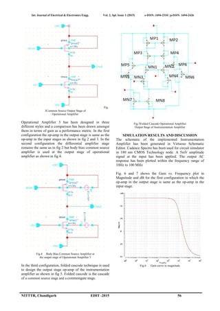
Fig.7 Gain curve in decibels
Fig. 8 and 9 shows the Gain vs. Frequency plot in
Magnitude and dB for the second configuration in which
the differential amplifier stage remains the same but body
bias common source amplifier is used at the output stage of
operational amplifier.
Fig.8
Gain curve in magnitude
.
Fig.9 Gain curve in decibels
Fig. 10 and 11 shows the Gain vs. Frequency plot in
Magnitude and dB for the third configuration,in which the
folded cascode technique is used to design the output stage
op-amp of the instrumentation amplifier.
Fig.10
Gain curve in magnitude
Fig.11 Gain curve in decibels
Tables II.shows the comparison for three different
configurations: basic op-amp, body bias op-amp and a
folded cascode op-amp.
TABLE II: Comparison between basic op-amp, body bias op-amp and a
folded cascode op-amp
The abrupt increase in the gain of the folded cascode
design as compared to the other two techniques is due to
the transistors sizing. The differential pair used is to keep a
check upon input voltage difference and is made to operate
in saturation region not in triode region.
Table III gives the aspect ratio(W/L) of the various
transistors used in the folded cascode configuration.
TABLE III: OUTPUT FOLDED CASCODE STAGE OP-AMP
TRANSISTOR
SIZING[2]
Transistors Aspect Ratio(W/L)
MN1,NM2 5μ/200n
MN3,MN4 3μ/200n
MN5,MN6 20μ/200n
MP1,MP2 20μ/200n
MP3.MP4 20μ/200n
Parameters Cascade
design
body
biased
cascode
design
Technology
(μm)
0.18 0.18 0.18
Supply voltage
(v)
1.8 1.8 1.8
Gain (dB) 1.24 1.8 33.67](https://image.slidesharecdn.com/id104-150526191342-lva1-app6892/85/Design-and-Analysis-of-CMOS-Instrumentation-Amplifier-3-320.jpg)
![Int. Journal of Electrical & Electronics Engg. Vol. 2, Spl. Issue 1 (2015) e-ISSN: 1694-2310 | p-ISSN: 1694-2426
NITTTR, Chandigarh EDIT -2015 58
MP5,MP6 50μ/200n
MN8 5μ/200n
MN7 10μ/200n
CONCLUSION
A comparative study and analysis for three different
configurations: basic op-amp, body bias op-amp and a
folded cascode op-amp has been done.Analysis shows that
the folded cascode design achieves comparatively high
gain as compared to thetwo stage Cascade Op-Amp design
and body biased design.
REFRENCES
[1] BehzadRazavi, Design of Analog CMOS Integrated Circuits,
Tata McGraw Hill Education.
[2]Goel, A. and Singh, G.,” Novel High Gain Low Noise CMOS
Instrumentation Amplifier for Biomedical Applications”,Machine
Intelligence and Research Advancement (ICMIRA), 2013
International Conference on ,PP. 392 – 396, 2013, IEEE
[3]S. Kirthy,“Performance Analysis of a High Gain CMOS
Instrumentation Amplifier for Biomedical Signal
Processing”,International Journal of Electronic and Electrical
Engineering.
ISSN 0974-2174 VOLUME 7, NUMBER 10 (2014), PP. 1133-1133
[4]Rajni, “Design of High Gain Folded-Cascode Operational
Amplifier Using 1.25 um CMOS Technology” International
Journal of Scientific & Engineering Research Volume 2, Issue 11,
November-2011 ISSN 2229-5518
[5]Yasin FM; Yap M.T and Reaz,M.B.I, “CMOS instrumentation
amplifier with offset cancellation circuitry for biomedical
applications,” In Proc. Of 5th
WESEAS,2006,spain,pp 168-171.
[6]Shojaei-Baghini, M. Lal, R.K Sharma and D.K,” An ultra low-
power CMOS instrumentation amplifier for biomedical
applications”, Biomedical circuits and systems,2004 IEEE
International Workshop On, S1/1-S1,2004,IEEE.
[7]Chih-Jen Yen; Wen-Yaw Chung and Mely Chen Chi, “Micro-
power low offset instrumentation amplifier IC design for
biomedical system applications” IEEE Transactions On Circuits
and Systems-I: Regular Papers, Vol.51,No.4, pp 691-699 april
2004.
[8] R. C. Yen and P. R. Gray, “A MOS switched-capacitor
instrumentation amplifier,” IEEE J.Solid-State Circuits, vol. SC-
17, pp. 1008–1013, Dec. 1982.
[9]Ramakant A. Gayakward, op-amps and linear integrated
circuits: Pearson Education.](https://image.slidesharecdn.com/id104-150526191342-lva1-app6892/85/Design-and-Analysis-of-CMOS-Instrumentation-Amplifier-4-320.jpg)

The document presents the design and analysis of a CMOS instrumentation amplifier utilizing three operational amplifiers to improve gain across different configurations: basic op-amp, body bias op-amp, and folded cascode op-amp. Implemented in 0.18µm CMOS technology, the study reveals that the folded cascode design significantly enhances gain compared to the other two configurations. Simulation results demonstrate the superior performance of the folded cascode design in achieving high gain, crucial for amplifying weak signals in various applications.