Download as PDF, PPTX
![Heterostructures
Heterojunction Bipolar Transistor
Thyristors
Introduction
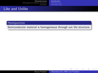
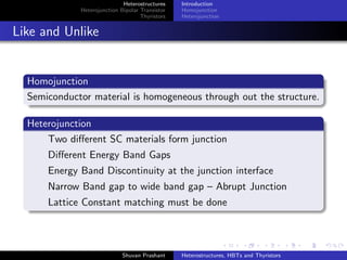
Homojunction
Heterojunction
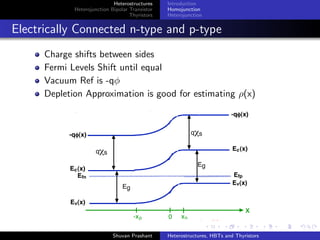
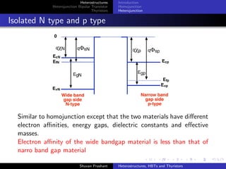
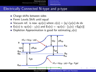
Electrically Connected N-type and p-type
Charge shifts between sides
Fermi Levels Shift until equal
Vacuum ref. is now -qφ(x) where φ(x) = (q/ )ρ(x) dx dx
Ec(x) is -qφ(x) - χ(x) and Ev(x) = -qφ(x) - [χ(x) +Eg(x)]
Depletion Approximation is good for estimating ρ(x)
Shuvan Prashant Heterostructures, HBTs and Thyristors](https://image.slidesharecdn.com/heterostructures-140616031444-phpapp01/85/Heterostructures-HBTs-and-Thyristors-Exploring-the-different-11-320.jpg)
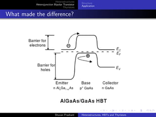

The document discusses heterostructures, heterojunction bipolar transistors (HBTs), and thyristors. It begins by explaining homojunctions and heterojuctions, how they differ in material composition and resulting energy band structures. It then describes HBTs, noting they can achieve higher speeds than bipolar junction transistors (BJTs) due to reduced injection of minority carriers into the emitter. Finally, it discusses thyristors, four-layer pnpn semiconductor devices that can operate in either conducting or blocking states, and diacs, bidirectional thyristor variants used in alternating current switching applications.


