Downloaded 145 times
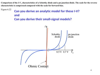

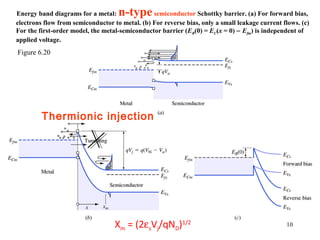
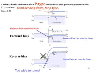
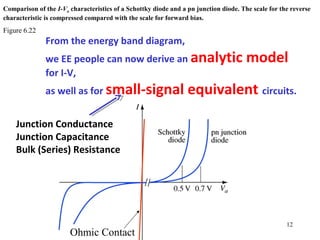

This document discusses metal-semiconductor contacts and junctions. It provides figures from the textbook explaining the band diagrams and behavior of Ohmic contacts, Schottky contacts, and pn junction diodes. It addresses questions about deriving analytic models for the I-V characteristics and small-signal models of these devices based on their band structures and transport mechanisms.


![Balance volumenes de_lodo_amoco_-_drilling_fluids_manual[1]](https://cdn.slidesharecdn.com/ss_thumbnails/balancevolumenesdelodoamoco-drillingfluidsmanual1-130803182906-phpapp01-thumbnail.jpg?width=640&height=640&fit=bounds)


