Introduction to PNJunction
• • A PN junction is formed by joining P-type
and N-type semiconductors.
• • It is the fundamental unit of diodes,
transistors, LEDs, and solar cells.
• • Controls how current flows in electronic
devices.
• • Key concepts: diffusion, depletion region,
biasing, energy bands.
3.
P-type Semiconductor
• •Doped with trivalent impurities (Boron,
Gallium).
• • Creates 'holes' which act as positive charge
carriers.
• • Majority carriers: Holes
• • Minority carriers: Electrons
• • Used to form one side of the PN junction.
4.
N-type Semiconductor
• •Doped with pentavalent impurities
(Phosphorus, Arsenic).
• • Provides extra electrons for conduction.
• • Majority carriers: Electrons
• • Minority carriers: Holes
• • Forms the other half of the PN junction.
5.
Formation of PNJunction
• • When P and N materials are joined,
electrons diffuse to P-side and holes diffuse to
N-side.
• • This creates a region with no free carriers
called the depletion region.
• • Immobile ions remain, forming an internal
electric field.
• • This electric field opposes further carrier
movement.
6.
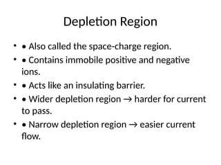
Depletion Region
• •Also called the space-charge region.
• • Contains immobile positive and negative
ions.
• • Acts like an insulating barrier.
• • Wider depletion region → harder for current
to pass.
• • Narrow depletion region → easier current
flow.
7.
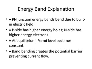
Energy Band Explanation
•• PN junction energy bands bend due to built-
in electric field.
• • P-side has higher energy holes; N-side has
higher energy electrons.
• • At equilibrium, Fermi level becomes
constant.
• • Band bending creates the potential barrier
preventing current flow.
8.
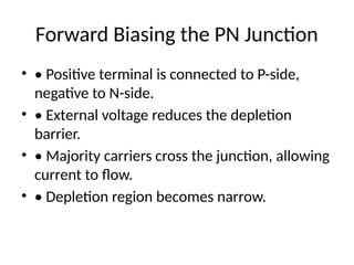
Forward Biasing thePN Junction
• • Positive terminal is connected to P-side,
negative to N-side.
• • External voltage reduces the depletion
barrier.
• • Majority carriers cross the junction, allowing
current to flow.
• • Depletion region becomes narrow.
9.
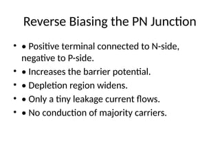
Reverse Biasing thePN Junction
• • Positive terminal connected to N-side,
negative to P-side.
• • Increases the barrier potential.
• • Depletion region widens.
• • Only a tiny leakage current flows.
• • No conduction of majority carriers.
10.
I–V Characteristics ofPN Junction
• Forward Bias:
• • Current increases exponentially after
threshold voltage (≈ 0.7V for Si).
• Reverse Bias:
• • Very small leakage current.
• • Breakdown occurs at high reverse voltage
(Zener or Avalanche breakdown).
11.
Applications of PNJunction
• • Rectifiers (AC to DC Conversion)
• • LEDs and Laser Diodes
• • Photodiodes and Solar Cells
• • Transistors (BJT, MOSFET)
• • Voltage Regulators (Zener)
• • Signal Clipping and Clamping Circuits