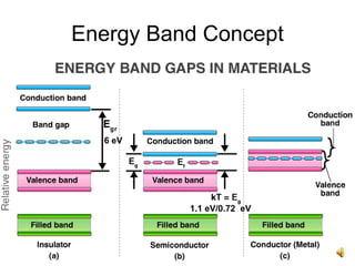
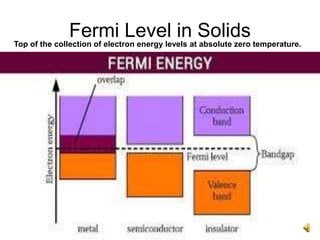
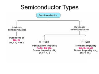
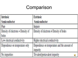
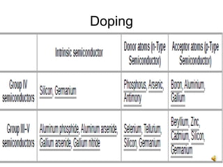
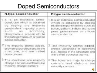
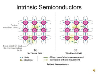
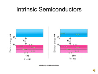
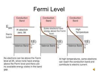
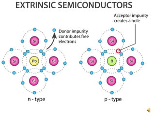
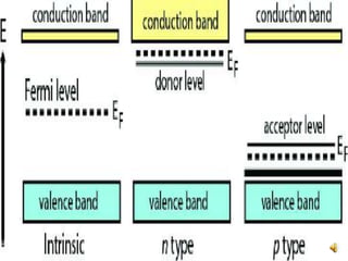
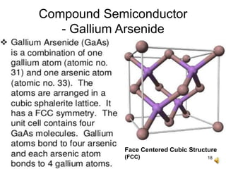
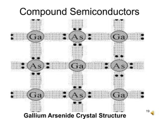
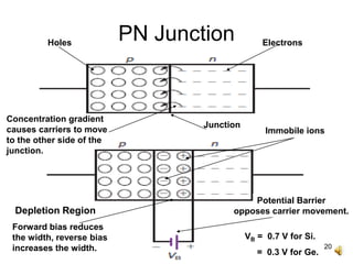
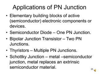
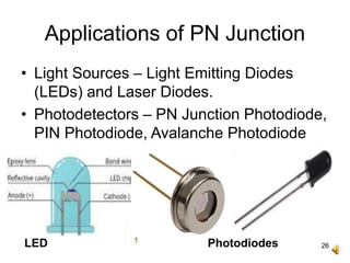
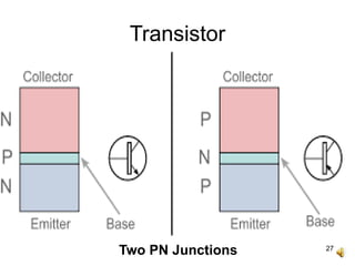
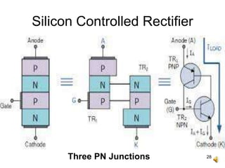
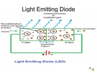
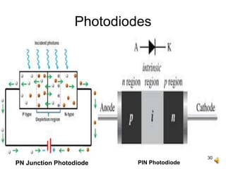
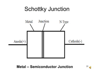
1
Semiconductors
MEC
2
Contents
• Definitions.
• Energy Band Diagrams.
• Intrinsic Semiconductors.
• Extrinsic Semiconductors.
• Comparison.
• PN Junction.
• PN Junction Applications.
3
Definitions
• Energy Band : The range of energies
possessed by an electron in a solid.
• Valence Electron : Electrons in the
outermost orbit of an atom.
• Valence Band : Range of energies
possessed by valence band electrons.
• Conduction Band : Range of energies
possessed by free electrons.
4
Definitions
• Fermi Level :
- highest energy level that an electron can
occupy at the absolute zero temperature.
- lies between valence and conduction
bands at absolute zero temperature.
- tends to change as solids are warmed.
- value of Fermi level at absolute zero
temperature known as Fermi energy.
5
Definitions
• Forbidden Energy Gap :
- gap between valence band and
conduction band.
- electron can be moved from valence
band to conduction band by applying
energy more than forbidden energy
gap.
• Hole : absence of an electron, +ve charge.
6
Energy Band Concept
6 eV
1.1 eV/0.72 eV
7
Fermi Level in Solids
Top of the collection of electron energy levels at absolute zero temperature.
8
Semiconductors
• Resistivity: 10-5 to 106 Ωm.
• Conductivity: 105 to 10-6 mho/m.
• Temperature coefficient of resistance:
Negative.
• Current Flow: Due to electrons and holes.
• Materials: Silicon, Germanium, Gallium
Arsenide.
9
Semiconductor Types
10
Comparison
11
Doping
12
Doped Semiconductors
13
Intrinsic Semiconductors
14
Intrinsic Semiconductors
15
Fermi Level
16
17
18
Compound Semiconductor
- Gallium Arsenide
Face Centered Cubic Structure
(FCC)
19
Compound Semiconductors
Gallium Arsenide Crystal Structure
20
PN Junction
Concentration gradient
causes carriers to move
to the other side of the
junction.
Potential Barrier
opposes carrier movement.
Junction
Depletion Region
Forward bias reduces
the width, reverse bias
increases the width.
Immobile ions
VB = 0.7 V for Si.
= 0.3 V for Ge.
Holes Electrons
21
Biasing a PN Junction
• Forward Bias – Positive terminal of the
battery connected to the P - type material,
negative terminal of the battery connected
to N - type material.
• Current flow during forward bias.
• Reverse Bias – Positive terminal of the
battery connected to the N - type material,
negative terminal of the battery connected
to P - type material.
• No current flow during reverse bias.
22
Biased PN Junctions
23
24
Comparison
25
Applications of PN Junction
• Elementary building blocks of active
(semiconductor) electronic components or
devices.
• Semiconductor Diode – One PN Junction.
• Bipolar Junction Transistor – Two PN
Junctions.
• Thyristors – Multiple PN Junctions.
• Schottky Junction – metal –semiconductor
junction, metal replaces an extrinsic
semiconductor material.
26
Applications of PN Junction
• Light Sources – Light Emitting Diodes
(LEDs) and Laser Diodes.
• Photodetectors – PN Junction Photodiode,
PIN Photodiode, Avalanche Photodiode
etc.
LED Photodiodes
27
Transistor
Two PN Junctions
28
Silicon Controlled Rectifier
Three PN Junctions
29
Light Emitting Diode
30
Photodiodes
PN Junction Photodiode PIN Photodiode
31
Schottky Junction
Metal – Semiconductor Junction
32
Thank You

EST 130, Semiconductors